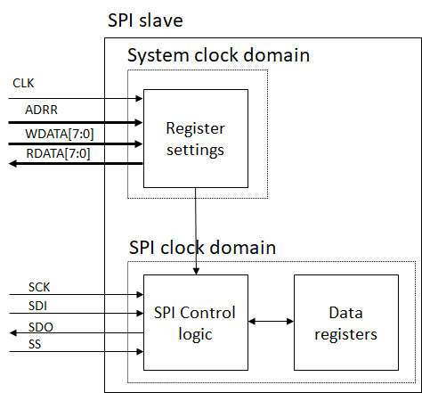
Dear all,

I have a question about idea for SPI slave design. My system is as
attachment.

There are 2 clock domains: System Clock and SPI clock. Those clocks are
asynchronous.
System clock is used to write configurations for SPI operation, such as:
CPOL, CPHA,... SPI domain needs to read configuration from System Clock
and uses those configuration for its operation.

May I ask about the synchronization idea for design. Which one in the
following is better?
1. Write configurations in system clock domain, and SPI clock domain can
read configurations from system clock domain directly, no need to
synchronize

This way does not use any synchronization circuit, but there is a
limitation for user: User must set configuration first, then wait a time
for configuration is stable, then issue a SPI transaction.

2. Synchronized SPI signals (SCK, SDI, SS) from SPI clock domain into
system clock domain. All SPI operations will operate at system clock
domain.

This method is more safer than method 1, but I do not know which
synchronizer is suitable? 2 Flip Flops synchronizer for each SPI signal
(SCK, SDI, SS) is reasonable or not?

Please give me a help.

Thank you!
Attached files:
-

spi_slave_design.png
6 KB
I would prefer method 1.

Configuration ist written during system initialisation. If you change
SPI settings during a SPI transfer the transfer fails in both cases.
So any SPI traffic during initialisation must be forbidden either way.
What are the frequencies of sys_clk and spi_clk?

If sys_clk-frequency is at least twice as high as the spi_clk-frequency
i would use the sys_clk as the only real clock in this system - only one
clock-domain. In this case i would synchronize the spi-signals by using
FFs clocked with sys_clk.

If sys_clk-frequency is not twice as high as the spi_clk-frequency i
would use two clock-domains. The synchronization between the
clock-domains can be implemented by using dp-rams/fifos.
Schlumpf wrote:
> I would prefer method 1.
>
> Configuration ist written during system initialisation. If you change
> SPI settings during a SPI transfer the transfer fails in both cases.
> So any SPI traffic during initialisation must be forbidden either way.

Thank you Mr.Schlumpf for your idea!

I would consider more about the limitation for user if I apply method 1.
Attached files:
-

sys_clk-domain_sync.png
14 KB
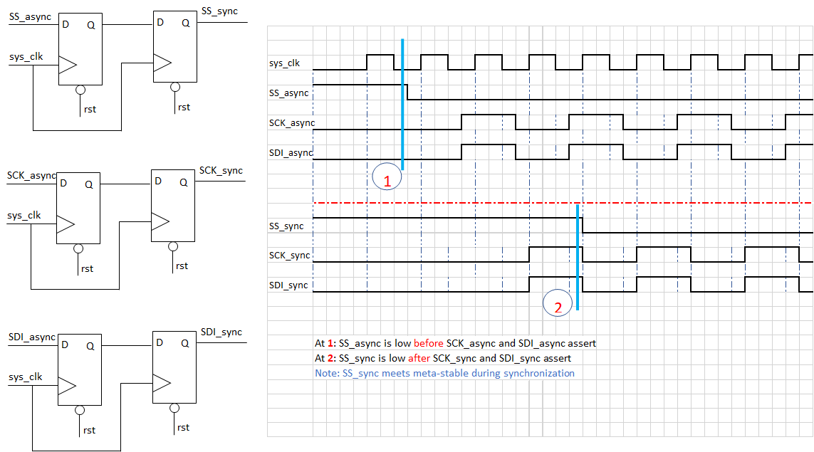
freduardo wrote:
> What are the frequencies of sys_clk and spi_clk?
>
> If sys_clk-frequency is at least twice as high as the spi_clk-frequency
> i would use the sys_clk as the only real clock in this system - only one
> clock-domain. In this case i would synchronize the spi-signals by using
> FFs clocked with sys_clk.
>
> If sys_clk-frequency is not twice as high as the spi_clk-frequency i
> would use two clock-domains. The synchronization between the
> clock-domains can be implemented by using dp-rams/fifos.


Thank you Mr.freduardo for your idea.

> What are the frequencies of sys_clk and spi_clk?


Now, I consider sys_clock-frequency is at least twice as high as the
spi_clk-frequency, so I prefer to your idea of one clock domain: sys_clk
as the only real clock in this system.

> In this case i would synchronize the spi-signals by using
> FFs clocked with sys_clk.


You meant: we can synchronize each SPI signal (SS, SCK, SDI) by using 2
FFs clocked with sys_clk. Is it correct?

If it is correct, please see attachment named sys_clk-domain_sync.png.
Is there any problem if we use 3 separated circuits (each circuit is
2FFs) for synchronization? The problem is shown in
sys_clk-domain_sync.png as an example.
Jack B. wrote:
> I prefer to your idea of one clock domain: sys_clk as the only real
> clock in this system.
>> In this case i would synchronize the spi-signals by using FFs clocked
>> with sys_clk.
Thats the best and reproducable way.

> I consider sys_clock-frequency is at least twice as high as the
> spi_clk-frequency
A hint: factor 2 is a theoretical value. I suggest to make the system
clock far much higher than the SPI clock. Otherwise you may encounter
weird effects now and then...

> You meant: we can synchronize each SPI signal (SS, SCK, SDI) by using 2
> FFs clocked with sys_clk. Is it correct?
Yes, do so.
Attached files:
-

sys_clk-domain_sync.png
14 KB

Lothar M. wrote:

> Thats the best and reproducable way.

Thank you for this advice!

> A hint: factor 2 is a theoretical value. I suggest to make the system
> clock far much higher than the SPI clock. Otherwise you may encounter
> weird effects now and then...

I have no experience about this. I read from this link(StackExChange),
they said that frequency of system clock and SPI clock should be "at
least 2:1 but preferably 4:1 or more"

https://electronics.stackexchange.com/a/276235/138472

My SPI clock has maximum frequency around 16 MHz. If so, can my system
clock be 64 Mhz (4:1)?

I need your advice!

>> You meant: we can synchronize each SPI signal (SS, SCK, SDI) by using 2
>> FFs clocked with sys_clk. Is it correct?
> Yes, do so.

Thank you!

I appreciate if you can answer my previous question. It is not a digging
question. I am a newbie of synchronization method, so I am not clear
about synchronization mechanism so much.

>> If it is correct, please see attachment named sys_clk-domain_sync.png.
>> Is there any problem if we use 3 separated circuits (each circuit is
>> 2FFs) for synchronization? The problem is shown in
>> sys_clk-domain_sync.png as an example.
Jack B. wrote:
> My SPI clock has maximum frequency around 16 MHz. If so, can my system
> clock be 64 Mhz (4:1)?
Those are reasonable values. Althoug 16MHz is a fairly fast SPI. You
should have a close look at the layout and the termination of the SPI
signals.
Do you also send data from Slave to Master (MISO)?
If yes, you should have a look at the setup-time of the master.

The master sends first data with the first (rising) edge of SCK and
reads data with the first (falling) edge of CLK.

If you generate the MISO data with the synchronized SCK-Signal (writing
edge) you add a lot of delay which can lead to a setup violation at the
master DI.

e.g.:

SPI-SCK: 16 MHz means clock period = 62ns.
System-clock: 64MHz means clock period = 16ns

2-stage synchronizer and one additional clock for edge detection of the
SCK-Signal lead to a delay of 3 system clocks (3 x 16ns = 48 ns) between
arrival of the unsynchronized SCK and valid output of MISO.
The master expects MISO to be valid a certain time (tsu) BEFORE the
reading edge of unsynchronized  SCK.

Time between writing edge and reading edge of SCK is SPI-SCK/2 (31ns).
Time when data must be valid at master MISO Pin is (31ns - tsu) after
master sends the writing edge of SCK.


Keep that in mind!
Lothar M. wrote:
> Jack B. wrote:
>> My SPI clock has maximum frequency around 16 MHz. If so, can my system
>> clock be 64 Mhz (4:1)?
> Those are reasonable values. Althoug 16MHz is a fairly fast SPI. You
> should have a close look at the layout and the termination of the SPI
> signals.

Thank you Mr.Lothar Miller.
Let me consider more about the ratio of frequency between system clock
and SPI clock. Because my SPI clock is fairly fast (16 MHz), I should
select an appropriate frequency for system clock.
Jack B. wrote:
> I should select an appropriate frequency for system clock.
According to Schlumpfs considerations and calculations (which are
mandatory) I would use somewhat in the 100MHz range...
Attached files:
-

sys_clk-domain_sync.png
14 KB

Schlumpf wrote:
> Do you also send data from Slave to Master (MISO)?

Yes, I also send data from Slave to Master (MISO)

> If yes, you should have a look at the setup-time of the master.
>

Thank you for your explanation! It is very clear!
I understood that if I select system clock is 64 MHz, SPI clock is 16
MHz,
the master can not capture data on MISO.

From your explanation, I understood that I should select frequency of
system clock which must be higher than SPI clock as much as possible.
This will prevent the problem of capturing MISO at Master side.

For example, if I select SPI-SCK: 16 MHz, System-clock: 128MHz (system
clock: SPI clock = 8:1)

SPI-SCK: 16 MHz -> clock period = 62ns.
System-clock: 128MHz -> clock period = 8ns

At system clock handler: 2-stages FF + 1 edge detection = 24 ns (8*3ns)
At 24ns, MISO is valid if I used 2-stage FF synchronizer.

At Master with unsynchronized SCK: data input from slave (MISO) must be
valid at SPI-SCK/2 - tsu (31ns - tsu)

I think this ratio (8:1) is more feasible for Master side than (4:1)
I will consider more about the ratio if I apply method 2.

By the way, do you know the answer for my following question? Assuming
that I can solve the ratio between system clock and SPI clock. I am not
sure whether I can meet a problem about the 2 FFs sync if I use method 2
or not. My question relates to synchronization. It is as follows.

> Is there any problem if we use 3 separated circuits (each circuit is
> 2FFs) for synchronization? The problem is shown in
> sys_clk-domain_sync.png as an example.
Refer to the datasheet of the master to geht the value for tsu.
Then you can calculate the maximum time you can "waste" within your
slave.

(SPI-SCK / 2) - tsu.

And keep in mind that you have additional signal delay from the SCK-Pin
of your FPGA to the first sampling register. And also from the
data-output-register to the MISO-Pin of the FPGA.
This times must be added...

Your question:
Not clear what you mean.
Every signal has its own two registers. There is no other way..
You cannot combine different signals on a "shared" sample register.
If timing goes to the edge due to using 2 flipflops, then use only one.
With 100MHz thats no problem when it is really only 1 flipflop. So
register duplication should be disabled for that flipflop. Otherwise you
may have different values for the incoming signal in your design during
one clock cycle...

And one word to meta stability: nowadays flipflops are so fast, that it
meta stability may be an issue when your system clock goes up in the
300MHz range upwards (which is very, very unlikely).

Instead of meta stability you have the commen problem of different
length of routes and therefore different propagation time to different
flipflops on the chip, so without synching diefferent flipflops may see
diferent values of the same signal at the next clock edge. Thats the
common and major problem.

Just have a look at the pictures there:
http://www.lothar-miller.de/s9y/categories/35-Einsynchronisieren
Maybe Google translate can help you out, its German...
:
Edited by Moderator
Schlumpf wrote:

> Your question:
> Not clear what you mean.

My question is simple, but I do not know whether it can occur. If it
occurs, we can solve it or not.

1. At SPI clock domain: SS change from High to Low, then SCK starts to
change (L->H->L->...)
2. At system clock domain: We use 2 FFs clocked by system clock to
synchronize SS, and 2 FFs clocked by system clock to synchronize SCK.
3. At system clock domain: Synchronized SS meets mesta-stable problem,
synchronized SCK is normal (it does not meet meta-stable)
4. At system clock domain: Because of meta-stable of SS signal, the
order of SS and SCK at system clock domain is not same as SPI clock
domain. It is as below

SCK starts to change (L->H->L->...), then SS change from High to Low

5. Compare to SPI clock domain and system clock domain, the order of
"orgiginal" SPI signals and "synchronized" SPI signals are changed
SPI domain: SS change from High to Low, then SCK starts to change
(L->H->L->...)
System clock domain: SCK starts to change (L->H->L->...), then SS change
from High to Low
Lothar M. wrote:
> If timing goes to the edge due to using 2 flipflops, then use only one.
> With 100MHz thats no problem when it is really only 1 flipflop. So
> register duplication should be disabled for that flipflop. Otherwise you
> may have different values for the incoming signal in your design during
> one clock cycle...
>
> And one word to meta stability: nowadays flipflops are so fast, that it
> meta stability may be an issue when your system clock goes up in the
> 300MHz range upwards (which is very, very unlikely).

> Instead of meta stability you have the commen problem of different
> length of routes and therefore different propagation time to different
> flipflops on the chip, so without synching diefferent flipflops may see
> diferent values of the same signal at the next clock edge. Thats the
> common and major problem.
>
> Just have a look at the pictures there:
> http://www.lothar-miller.de/s9y/categories/35-Einsynchronisieren
> Maybe Google translate can help you out, its German...

I read your site. It is very useful.
Thank you for your detail explanation about meta-stability problem.
I have some basic understanding about meta-stable and synchronization.
But in this thread, I need the advice for some issues about
synchronization that I can not solve by myself.
Jack B. wrote:
> My question is simple, but I do not know whether it can occur. If it
> occurs, we can solve it or not.

Ahh, now I understand.

Yes this can theoretically occur....
But you can avoid this by proper constraining.

Between the inputs of the PFGA and the first sample register are
signal delays. SS-->SSreg (tss) and SCK-->SCKreg (tsck).
If tss is large and tsck is short it could happen that SCK "arrives"
before SS at the sample-registers which leads to mal funtion.

BUT:
In SPI-Domain there is a time between SS active and first edge of SCK.
If this time is larger then the skew between tss and tsck you will not
run in problems (add a little margin for internal skew of the clock to
the sample-registers).

Now the metastability problem:
If SS arrives earlier than SCK at the sample-register you should not run
into trouble.

What can happen?
1. sampling edge is between SS-low and SCK-edge
--> SS sampled first, SCK sampled later --> Fine

2. sampling edge is during falling edge of SS:
--> SSreg can be "high" or "low"..
But it is sampled correctly with the next sampling edge. And this is the
earliest edge SCK can be sampled with. So SSreg and SCKreg change at the
same time. Which is fine.
Two possibilities when SS is metastable:


clk ___|----|____|----|____|----|____|----|__

SS  -------------|___________________________

SCK ________________|------------------------

SSreg -----------XX--------|_________________

SCKreg ____________________|-----------------


clk ___|----|____|----|____|----|____|----|__

SS  -------------|___________________________

SCK ________________|------------------------

SSreg -----------XX__________________________

SCKreg ____________________|-----------------


both are fine... :-)
Schlumpf wrote:
> Jack B. wrote:
>> My question is simple, but I do not know whether it can occur. If it
>> occurs, we can solve it or not.
>
> Ahh, now I understand.
>

Thank you Mr.Schlumpf for your clear answer. I satisfy with this answer.

Now, I can understand the synchronization of SS and SCK has no problem
by "proper constraint". "Proper constraint" is the time between SS
active and the first edge of SCK.

> What can happen?

From your analysis for 2 possible cases, I understood case 1 is normal
case (meta-stable does not occur), case 2 is abnormal case (meta-stable
occurs), but it is fine for 2 cases (no problem can happen after
synchronization)!
Thank you for detail analysis!

Now, I am considering to synchronize SS, SCK, SDI from SPI clock domain
to system clock domain by 2 FFs in my design. There is a specific
requirement in my design, so I should apply method 2.

At the first view, SCK and SDI synchronization by 2 FFs do not meet any
issue even if there is meta-stable like SCK and SS synchronization.

For example
********
+ Setting: CPOL=0, CPHA=1 case. System clock : SPI clock = 8:1, it means
SPI-clock/2 (SPI-clock half cycle) = 4 cycles of system clock

+ At SPI clock domain: SDI is changed at rising edge of SCK, SPI slave
will capture SDI data at falling edge of SCK.
+ At system clock domain: 4 cases can occur

- (1) No meta-stable problem for both synchronized SCK and SDI.
Synchronized SDI and SCK is same as SPI clock domain.
Synchronized SDI is changed before falling edge of synchronized SCK ~5
cycles of system clock.
(4 cycles of system clock for SPI-clock/2 + 1 cycle of system clock for
edge detection SCK). At falling edge of synchronized SCK, synchronized
SDI is stable.

- (2) Meta-stable at SCK, SDI is normal (no meta-stable)
Synchronized SDI is changed before falling edge of synchronized SCK ~6
cycles of system clock.
(4 cycles of system clock for SPI-clock/2 + 1 system clock for
meta-stable of SCK + 1 cycle of system clock for edge detection SCK). At
falling edge of synchronized SCK, synchronized SDI is stable.

- (3) No meta-stable at SCK, SDI is abnormal (meta-stable)
Synchronized SDI is changed before falling edge of synchronized SCK ~4
cycles of system clock.
(4 cycles of system clock for SPI-clock/2 - 1 system clock for
meta-stable of SDI + 1 cycle of system clock for edge detection SCK). At
falling edge of synchronized SCK, synchronized SDI is stable.

- (4) Meta-stable problem for both synchronized SCK and SDI.
It is same as (1)

That is my consideration for SCK and SDI synchronization.
If you think it has any problem, please give a comment. Thank you so
much.
:
Edited by User
Just to clarify things: the flipflops in up-to-date FPGA recover so fast
that metastability is not an issue unless your system clock goes up to
the half GHz range.
See there:
https://resources.altium.com/pcb-design-blog/reducing-metastability-in-fpga-designs

Synchronizing is just and only to make sure that different propagation
paths all have the same logic level at the next clock edge.
:
Edited by Moderator
Lothar M. wrote:
> Just to clarify things: the flipflops in up-to-date FPGA recover so fast
> that metastability is not an issue unless your system clock goes up to
> the half GHz range.
> See there:
>
https://resources.altium.com/pcb-design-blog/reducing-metastability-in-fpga-designs
>

Thanks Mr.Lothar Miller for this information. So far, I have not known
this.

As my understanding, if we have an signal which is asynchronous with a
clock domain, we need to synchronize the signal to avoid meta-stability.
But I do not know the fast FlipFlops can reduce the meta-stability
problem!


> Synchronizing is just and only to make sure that different propagation
> paths all have the same logic level at the next clock edge.

Sorry for my lack knowledge of this matter. I do not understand this
matter well. Let me investigate more about the thing that you mentioned.
I think it´s not clear to you what metastability means...

Every register has a so called setup-time. This is the time the input
must be stable, BEFORE the edge of the clock.
If there is a change of the input during this time, the output of the
register can become metastable for a short time. So you cannot say if it
is high or low during this time. After this time (1-2ns) the output
becomes stable on high or low but it is not predictable if high or low.

So: Metastability only lasts for a very short time and after this time
the register is stable but not predictable on which logic level.

If you feed a register with a asynchronous signal you cannot guarantee
that there is no signal change within the setup-time.
Therefore you add a synchronization register. Even if there is a
violation of the setup time and a metastability occurs, the output of
the samping register is stable on the following clock edge.

Jack B. wrote:
>> Synchronizing is just and only to make sure that different propagation
>> paths all have the same logic level at the next clock edge.
>
> Sorry for my lack knowledge of this matter. I do not understand this
> matter well. Let me investigate more about the thing that you mentioned.

E.g.
Your design contains a state machine which is controlled by an
asynchronous signal.
So this signal can have influence on multiple registers. It passes some
combinatorial logic until it reaches the input of each of the registers.

So let´s say the signal has influence on two registers.
The delay from FPGA-input to Reg1 is 5ns and to Reg2 8ns.
When this external signal chances 7ns before the clock-edge it arrives
2ns BEFORE the edge on Reg1 and 1ns AFTER the edge on Reg2.
Reg1 is changed but Reg2 is not changed. This can lead to mal funtion of
the design.

If you use a snchronizing register the signal has only influence on ONE
single register which cannot lead to implausibility.
After this register the signal is synchronized to the clock domain and
every path to every target register is controlled by your synthesis tool
which ensures that no path is "longer" than one clock period.
Jack B. wrote:
> As my understanding, if we have an signal which is asynchronous with a
> clock domain, we need to synchronize the signal to avoid meta-stability.
> But I do not know the fast FlipFlops can reduce the meta-stability problem!
Take a sheet of paper and draw 2 flipflops behind each other. And supply
the same FPGA clock to both of them. The first one (that is connected to
the async external signal) may now and then be metastable for a certain
recovery time. Lets assume two different technologies and therefore 2
different recovery times from a metastable condition: 20ns for a very
slow technology and 1ns for a up-to-date technology.
If your FPGA clock cycle time is now 10ns (100MHz) then you may
encounter problems with the slow flipflops in the ancient technology,
because at the next clock cycle the slow ancient flipflop didn't recover
from the metastable condition and therefore the second flipflop doesn't
"know" which value it has to store.
But with the fast technology even if the first flipflop is metastable it
will recover from that well before the next relevant clock edge.
So flipflops that recover fast from a metastabe condition will never get
you into trobles because the second synchronizing flipflop will alsways
have a well defined level when reaching the next clock.
:
Edited by Moderator
Lothar M. wrote:
> Jack B. wrote:
>> As my understanding, if we have an signal which is asynchronous with a
>> clock domain, we need to synchronize the signal to avoid meta-stability.
>> But I do not know the fast FlipFlops can reduce the meta-stability problem!
> Take a sheet of paper and draw 2 flipflops behind each other. And supply
> the same FPGA clock to both of them. The first one (that is connected to
> the async external signal) may now and then be metastable for a certain
> recovery time. Lets assume two different technologies and therefore 2
> different recovery times from a metastable condition: 20ns for a very
> slow technology and 1ns for a up-to-date technology.
> If your FPGA clock cycle time is now 10ns (100MHz) then you may
> encounter problems with the slow flipflops in the ancient technology,
> because at the next clock cycle the slow ancient flipflop didn't recover
> from the metastable condition and therefore the second flipflop doesn't
> "know" which value it has to store.
> But with the fast technology even if the first flipflop is metastable it
> will recover from that well before the next relevant clock edge.
> So flipflops that recover fast from a metastabe condition will never get
> you into trobles because the second synchronizing flipflop will alsways
> have a well defined level when reaching the next clock.

Thanks Mr. Lothar Miller for detail example and explanation. I got your
idea.

For very slow technology, it takes 20ns to recover from metastable, but
FPGA clock is 10ns, so the second FlipFlop does not know which value it
should store.

For up-to-date technology, because the recovery time is just 1ns, so the
metastable can be recovered before the next clock edge of second
FlipFlop.

It is the main difference for recovery of metastable between slow
technology and up-to-date technology.
Schlumpf wrote:
> I think it´s not clear to you what metastability means...

>

Thanks Mr. Schlumpf for your explanation.
I have understood metastability problem so far. It is defined as below
link
http://www.asic-world.com/tidbits/metastablity.html

Just one thing that I forgot is: what value can be captured at the
second Flip Flop?

As your explanation, if metatability occurs at the first FlipFlop, it
can recover to stable in a very short time, but the value after recovery
is not predictable. It means, the value can be logic "1" or "0", we can
know which value after metastable recovery.

Because the recovery value after metastable at first FlipFlop can be "1"
or "0", so the captured value at second Flip Flop can be "1" or "0".
That is the point that I forgot.

> If you use a snchronizing register the signal has only influence on ONE
> single register which cannot lead to implausibility.
> After this register the signal is synchronized to the clock domain and
> every path to every target register is controlled by your synthesis tool
> which ensures that no path is "longer" than one clock period.

Ahh, now I can understand what Mr.Lothar Miller mentioned. Thank you for
your example and detail explanation!

Lothar M. wrote:

> Synchronizing is just and only to make sure that different propagation
> paths all have the same logic level at the next clock edge.
:
Edited by User
Please log in before posting. Registration is free and takes only a minute.
Existing account
Do you have a Google/GoogleMail account? No registration required!
Log in with Google account
Log in with Google account
No account? Register here.