Suchergebnisse für ""TL431""
in Figure 2-1 can further simplified by using a TL431 device by taking advantage of the internal error amplifier of the TL431 as this eliminates the need for an additional op amp. The TL431 CATHODE to REF feedback loop allows the insertion of a transistor to allow the regulation of VXto be V REF across R .SThis level of integration with the TL431 works for all 431 like products because they share the same architecture as shown in Figure 2-2. CATHODE REF + _ V ref ANODE Figure 2-2. TL431 Functional Block Diagram 2 Precision Current Sources and
in
„Bitte Review Schaltungentwurf für Ausgangsstufe für LiIon-Simulator“
·
Analoge Elektronik und Schaltungstechnik
·
07.11.2026 16:51
Bild
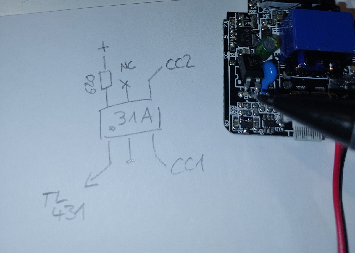
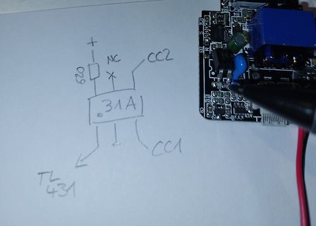
+ NC CC2 829 31A CC1 TL431 IC4 R4 D3 R12 R13 R15 AU
in
„USB-C PD (?) Netzteil“
·
Analoge Elektronik und Schaltungstechnik
·
25.10.2026 14:43
·
Fotos
Bild
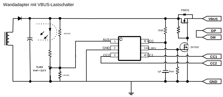
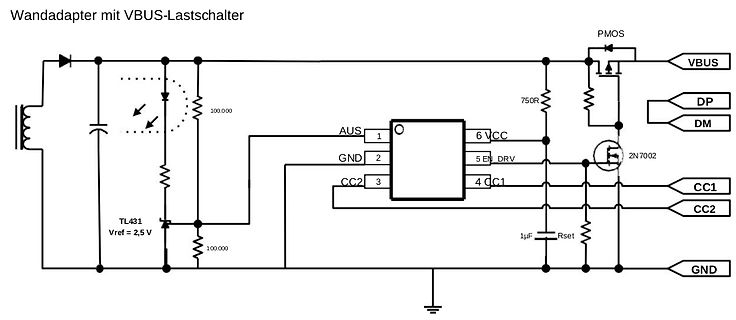
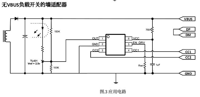
Wandadapter mit VBUS-Lastschalter, PMOS, VBUS, DP, DM, 750R, 2N7002, CC1, CC2, 1µF, Rset, GND, TL431 , Vref = 2,5 V, 100.000, AUS, GND, CC2, VCC, EN, DRV, CC1
in
„USB-C PD (?) Netzteil“
·
Analoge Elektronik und Schaltungstechnik
·
25.10.2026 14:02
·
Schaltpläne
Bild
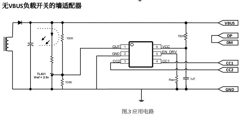
无VBUS负载开关的墙适配器
100K
TL431
Vref = 2.5v
100K
OUT 1
GND 2
CC2 3
VCC 6
EN DRV 5
CC1 4
750R
DP
DM
CC1
CC2
Rset
1uF
VBUS
GND
图.3 应用电路
in
„USB-C PD (?) Netzteil“
·
Analoge Elektronik und Schaltungstechnik
·
25.10.2026 14:27
·
Schaltpläne
Bild
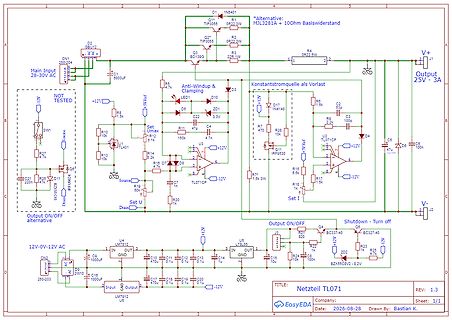
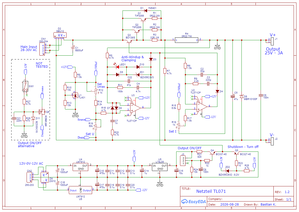
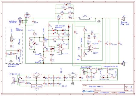
TL071CP, -12V, +12V, -5VRef, +5VRef, R4 1.5k, R5 4.7k, R6 1.5k, R7 4.7k, C2 47p, D5, D6, LED1, U1 TL431 , R8 9.2k, R10 13k, R11 13k, R12 4.7k, R13 4.7k, R14 6.6k, R15 6.6k, U3 TL071CP, Set Umax, Set I, Output ON/OFF alternative, 12V-0V-12V AC, CN2, C9 1000uF, C10 470u, C11 0.1u, C12 0.1u, C13 1u, C14
in
„Nebenprojekt: Analoges Labornetzteil inkl. Schaltplan und Messungen“
·
Projekte & Code
·
22.10.2026 02:18
·
Schaltpläne
Bild
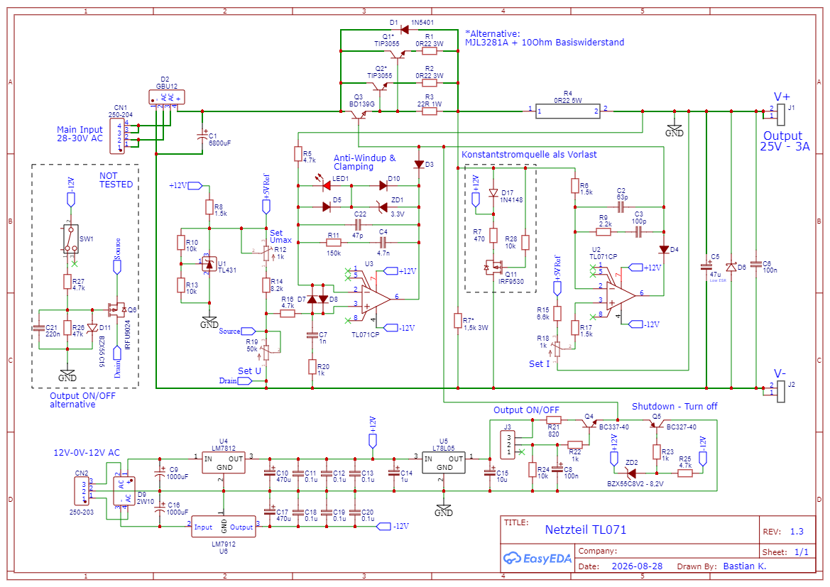
LED1, Anti-Windup & Clamping, Konstantstromquelle als Vorlast, D5, R5 4.7k, R8 1.5k, C2 100pF, U1 TL431 , R10 10k, R11 47p, U2 IRF9530, R16 0.6k, R15 1.5k, R9 2.2k, R14 9.2k, R17 4.7k, D7, D8, U3 TL071CP, -12V, R13 10k, C3 100n, R12 1.5k, R6 2.2k, C5 47u, C6 100n, Q4, Q5, BC337-40, BC327-40, R21 820,
in
„Nebenprojekt: Analoges Labornetzteil inkl. Schaltplan und Messungen“
·
Projekte & Code
·
30.10.2026 00:07
·
Schaltpläne
3 R11 47p R r R10 Umax V o 10k 2 R12 150k 4.7n + U2 D4 1 3 S 3 1k TL071CP C5 1 U1 1 U3 1 D6 C6 2 TL431 1 +12V 5 +12V 100n 5 7 7 47u MBR10100F R27 R13 R14 2 4.7k 10k 8.2k 2 R15 6 R16 D7 D8 6 6.6k 3 4.7k 3 Q6 8 4 GND 8 4 4 C21 R26 D11 2 -12V R17 -12V 220n 47k B 9 Source C7 TL071CP 3 1.5k X F R19 3 1n
in
„Nebenprojekt: Analoges Labornetzteil inkl. Schaltplan und Messungen“
·
Projekte & Code
·
22.10.2026 02:18
470 R28 r R10 Umax 10k o 10k 2 R12 150k 4.7n U2 D4 1 3 S 3 1k e TL071CP C5 1 U1 1 U3 R 1 D6 C6 2 TL431 1 +12V 5 5 +12V 100n 5 7 Q11 + 7 Low ESR R27 R13 R14 IRF9530 2 4.7k 10k 8.2k 2 6 R16 D7 D8 6 3 4.7k 3 Q6 R15 8 8 4 R7* 6.6k 4 C21 R26 D11 2 GND -12V 1,5k 3W R17 -12V 220n 47k B 9 Source C7 TL071CP
in
„Nebenprojekt: Analoges Labornetzteil inkl. Schaltplan und Messungen“
·
Projekte & Code
·
30.10.2026 00:07

 Bild
 Bild
 Bild
 Bild
 Bild