The SMBus modules include the following features: • Standard (up to 100 kbps) and Fast (400 kbps) transfer speeds. • Support for master, slave, and multi-master modes. • Hardware synchronization and arbitration for multi-master mode. • Clock low extending (clock stretching) to interface with faster masters
of compensation design is to shape at the location of the ESR zero. Determine C6 the converter transfer function to get a desired by the equation: loop gain. The system crossover frequency C2 R ESR where the feedback loop has the unity gain is C6 = important. Lower crossover frequencies result R3 in
goal of compensation design is to shape 2. Choose the compensation capacitor (C3) to the converter transfer function to get a desired achieve the desired phase margin. For loop gain. The system crossover frequency applications with typical inductor values, setting where the feedback loop has the unity gain
ihr mit Bestandsdesigns umgehen? Viele unterschätzen den Aufbau einer neuen Bibliothek und den Transfer von einem Tool in ein neues Tool. Ich habe das in einer Firma komplett durchexerziert und der Vorgang hat mit Abstand am meisten Aufwand und Zeit gekostet. Den Importern würde ich im kommerziellen
Reserved
ADDRESS_SIZE
DATA_SIZE
RX
Synch (0xSS)
STS
Adr_0
Adr_n
Data_0
Data_n
TX
ΔGT
ACK
ΔGT
ACK
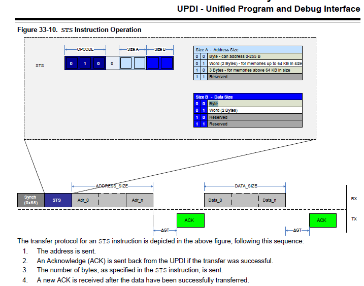
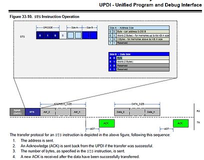
The transfer protocol for an STS instruction is depicted in the above figure, following this sequence:
1. The address is sent.
2. An Acknowledge (ACK) is sent back from the UPDI if the transfer was successful.
YUZ ® standard products shall ® also apply to such Bourns custom products. Users shall not sell, transfer, export or re-export any Bourns▯WYVK\J[Z▯VY▯[LJOUVSVN`▯MVY▯\ZL▯PU▯HJ[P]P[PLZ▯^OPJO▯PU]VS]L▯[OL▯ KLZPNU▯▯KL]LSVWTLU[▯▯WYVK\J[PVU▯▯\ZL▯VY▯Z[VJRWPSPUN▯VM▯U\JSLHY▯▯JOLTPJHS▯VY▯IPVSVNPJHS▯^LHWVUZ▯VY▯TPZZPSLZ
802.1h/RFC1042 frame encapsulation; Scattered DMA for optimal CPU off load on Zero Copy data transfer operations; Antenna diversity and selection (software managed hardware); Clock/power gating combined with 802.11-compliant power management dynamically adapted to curent connection condition providing
5 bEndpointAddress 0x81 EP 1 IN bmAttributes 2 Transfer Type Bulk Synch Type None Usage Type Data wMaxPacketSize 0x0040 1x 64 bytes bInterval 0 Endpoint
5 bEndpointAddress 0x02 EP 2 OUT bmAttributes 2 Transfer Type Bulk Synch Type None Usage Type Data wMaxPacketSize 0x0040 1x 64 bytes bInterval 0 [/c]
Harald K. schrieb im Beitrag #7881285: > 6502 hat exakt null MOV-Instruktionen. Dafür aber "transfer". Ist das besser? :)
SEI set interrupt disable STA store accumulator STX store X STY store Y TAX transfer accumulator to X TAY transfer accumulator to Y TSX transfer stack pointer to X TXA transfer X to accumulator TXS transfer X to stack pointer TYA transfer Y to accumulator [/code
oder doppelseitige Platinen Das Tonertransferverfahren hast du dir angesehen? Jeder, den den Transfer beherrscht, will aus guten Gründen nie wieder belichten...
kann sich so auf industriell gereinigte und beschichtete Platinen verlassen. Für erfolgreichen Transfer ist mehr nötig, deshalb scheitern ja so viele daran. Hier wird, vorrangig von denen, die es nicht schaffen, der totale Unfug erzählt, was den Transfer anbetrifft... Die Wahrheit ist: du kannst jeden
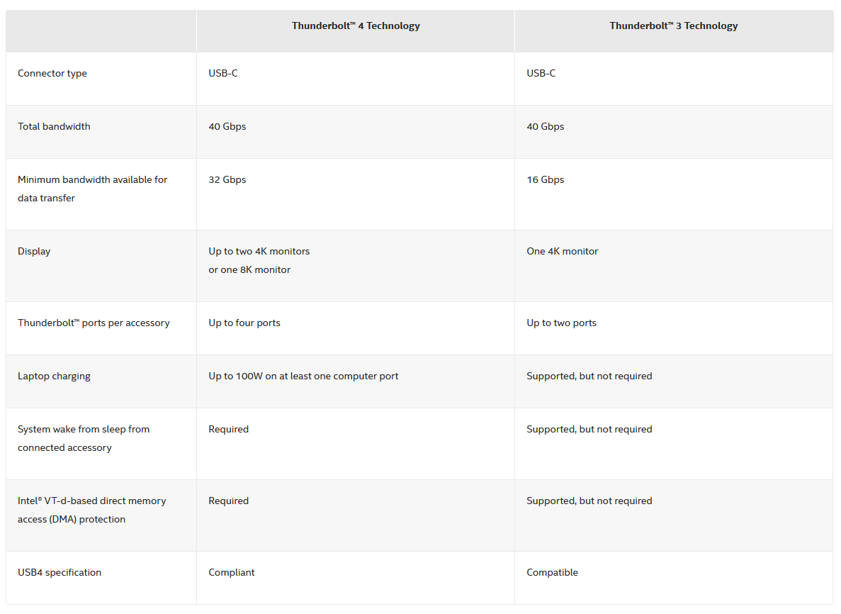
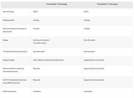
Connector type USB-C USB-C
Total bandwidth 40 Gbps 40 Gbps
Minimum bandwidth available for data transfer 32 Gbps 16 Gbps
Display Up to two 4K monitors or one 8K monitor One 4K monitor
Thunderbolt™ ports per accessory Up to four ports Up to two ports
Laptop charging Up to 100W on at least one computer
Data Modes 591 27.5.2 FSPI Bus Signal Mapping 592 27.5.3 Bit Read/Write Order Control 594 27.5.4 Transfer Modes 594 27.5.5 CPU-Controlled Data Transfer 594 27.5.5.1 CPU-Controlled Master Mode 595 27.5.5.2 CPU-Controlled Slave Mode 596 27.5.6 DMA-Controlled Data Transfer 596 27.5.6.1 GDMA Configuration
pin SS V –0.5 to +6.5 V Maximum I per I/O pin 15 mA OL Power dissipation (based on package heat transfer limitations, not device power consumption) 1.5 W NOTES: 1. Stresses above those listed under Absolute Maximum Ratings may cause permanent damage to the device. This is a stress rating only and functional
to base voltage VEBO IE= 10µA, IC= 0 5 V hFE11 V CE = 10V, C = 500mA *2 85 340 Forward current transfer ratio hFE2 V CE = 5V, B = 1A*2 50 *2 CollectortoemittersaturationvoltagVCE(sat) IC= 500mA, I B 50mA 0.2 0.4 V *2 Base to emitter saturation voltageVBE(sat) IB= 500mA, I a 50mA 0.85 1.2 V Transition
zu möglichen Fehlercodes oder -Ursachen? Darf man die Funktion aufrufen, wenn bereits ein DMA-Transfer aktiv und noch nicht abgeschlossen ist? Und warum überhaupt versuchst Du, einzelne Bytes an eine UART per DMA zu übertragen? Mit welcher Baudrate arbeitest Du?
Analyzer gemessene Rauschen ist deutlich geringer, trotzdem passiert es ab und zu, das während dem SPI Transfer der CS gezogen wird und dadurch der Slave nicht mehr im Sync mit dem Master ist, wie in dem glitch Bild zu sehen.
size 0x32 lma 0x1bc Loading section .text, size 0x1bc lma 0x0 Start address 0x0, load size 494 Transfer rate: 3952 bits in <1 sec, 30 bytes/write. Da diese 3 Schritte üblicherweise, bei jedem Start einer Simulationssitzung ausgeführt werden müssen, können sie zeilenweise in eine Textdatei (Vorschlag
This boundary condition can be represented as: k∂T +h(T −T ) = 0 (1.38) ∂n o where h is the “heat transfer coefficient” and Tois the ambient cooling fluid temperature. • Radiation Heat flux via radiation can be described mathematically as: ∂T ▯ 4 4▯ k ∂n +βk sb T −T o = 0 (1.39) where beta is the emissivity
github.com/STMicroelectronics/STM32CubeF0/tree/master/Projects/STM32F042K6-Nucleo/Examples/ADC/ADC_DMA_Transfer Dürfte sich bereits auf deinem PC befinden als Teil des STM32CubeF0.
wireshark direkt an die Capture-Schnittstelle anbindet; kopiere ich jetzt nicht. Oder den Datei-Transfer zu wireshark händisch machen. Wenn der Traffic dort ankommt die LAN-Schnitstelle(n) der FB abschnorcheln auf der der Traffic zum Reverse-Proxy gehen soll. Wenn das auch gut aussieht, dann auf
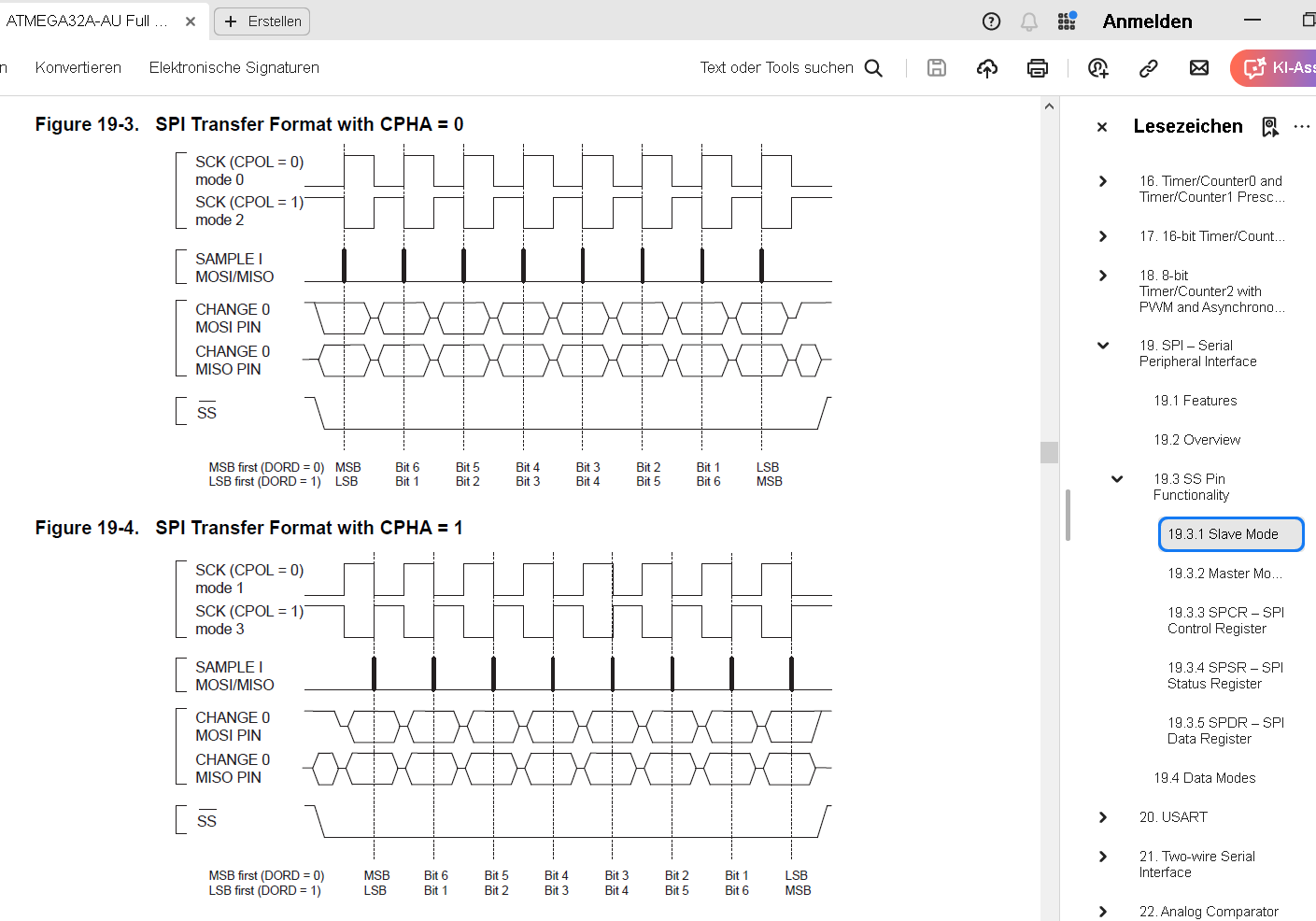
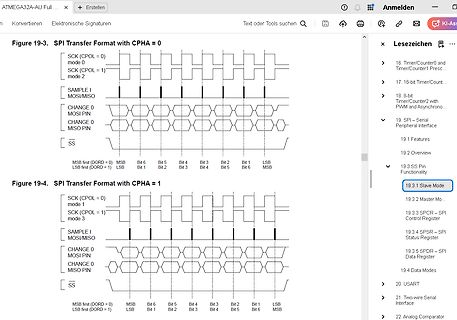
ATMEGA32A-AU Full... Anmelden Figure 19-3. SPI Transfer Format with CPHA = 0 SCK (CPOL = 0) mode SCK (CPOL = 1) mode 2 SAMPLE I MOSI/MISO CHANGE 0 MOSI PIN CHANGE 0 MISO PIN SS MSB first (DORD = 0) LSB first (DORD = 1) MSB Bit 6 Bit 5 Bit 4 Bit 3 Bit 2 Bit 1 LSB MSB Figure 19-4. SPI Transfer Format with CPHA = 1 SCK (CPOL = 0) mode SCK (CPOL = 1) mode 3 SAMPLE I MOSI/MISO CHANGE 0 MOSI PIN CHANGE 0 MISO PIN SS MSB first (DORD = 0) LSB first (DORD = 1) MSB Bit 6 Bit 5 Bit 4 Bit 3 Bit 2
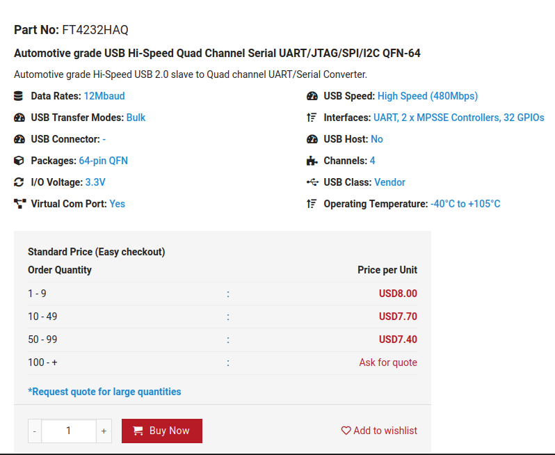
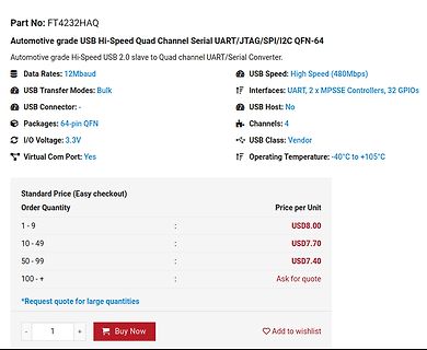
to Quad channel UART/Serial Converter.
Data Rates: 12Mbaud
USB Speed: High Speed (480Mbps)
USB Transfer Modes: Bulk
Interfaces: UART, 2 x MPSSE Controllers, 32 GPIOs
USB Connector: -
USB Host: No
Packages: 64-pin QFN
Channels: 4
I/O Voltage: 3.3V
USB Class: Vendor
Virtual Com Port: Yes
Operating Temperature
to 60%RH 10 − − Ω Zero cross voltage V I =8mA − − 35 V OX F VD(rms)=100V, AC50Hz S102S02 − − 10 TransferTurn-on time ton T (rms)=2A, Resistance loadF I =20mA ms charac- VD(rms)=200V, AC50Hz teristics S202S02 − − 10 T (rms)=2A, Resistance loadF I =20mA VD(rms)=100V, AC50Hz S102S02 − − 10 Turn-off time
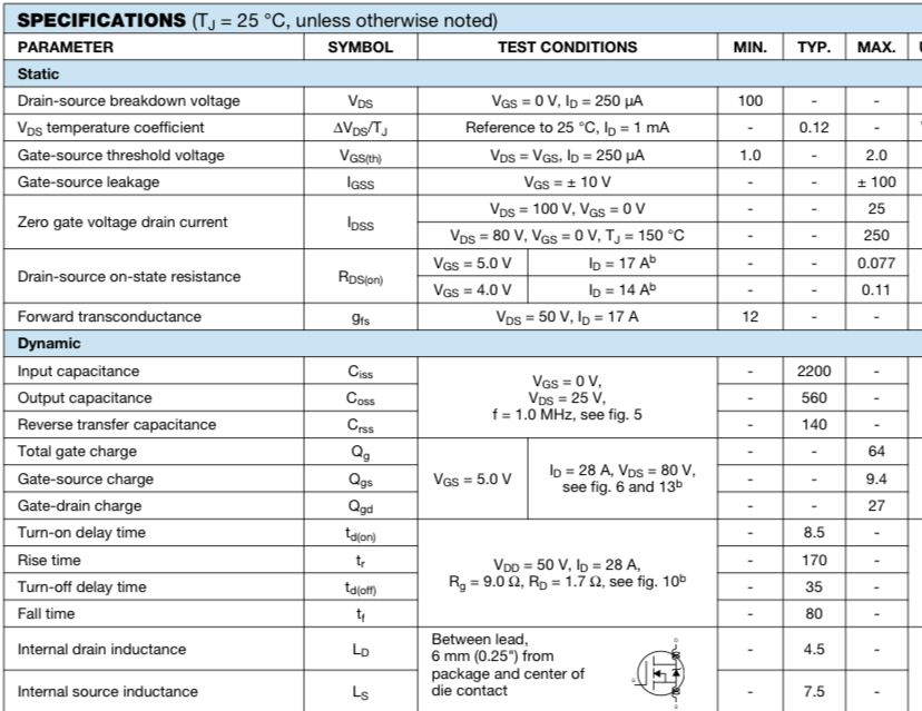
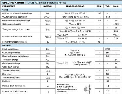
Voltage (V_GS(th)) Input Capacitance (C_iss) Output Capacitance (C_oss) Reverse Transfer Capacitance (C_rss) It's worth noting that without the specific datasheet, the exact values for these parameters cannot be provided for the EZ10N16. Availability The EZ10N16 MOSFET appears to
Fritzbox ins WEB schickt bzw. empfängt. Wireshark kann das nicht, da sehe ich nur den lokalen Transfer. Was ich gesehen habe tcpdump kann das auch nicht. Hab es jetzt mit der Fritzbox selber erledigt. Dort kann man zwar nicht filtern, aber den Mitschnitt kann man längenmäßig begrenzen. Das reicht
Fritzbox ins WEB schickt bzw. empfängt. Wireshark kann das nicht, > da sehe ich nur den lokalen Transfer. Was ich gesehen habe tcpdump kann > das auch nicht. Sowohl Wireshark als auch tcpdump können das natürlich prinzipiell. Man müsste sie halt nur auf der Fritzbox zum Laufen bringen und nicht
TFT-LCD module includes LVDS receiver. LVDS is a differential signal technology for high-speed data transfer LCD interface. LVDS Transmitter shall be THC63LVDM83A (THINE) or e.uivalent Pin No. Symbol Pin Description 1 VDD Power supply, 3.3V (typical) 2 VDD Power supply, 3.3V (typical) 3 GND Ground Selection
STM32, ein paar Jahre später, war dagegen nur eine kleine Fingerübung, nicht zuletzt wegen dem DMA-Transfer auf die SPI-Schnittstelle. Seitdem nutze ich eigentlich von Atmel nur noch die Tiny13A oder einen Mega328P in einem Arduino Uno wegen der einfachen Verfügbarkeit für einfache LED Spielereien und wegen
a positive supply via a pull-up resistor when connected to the output stages of a device. Data transfer may be initiated only when the bus is not busy. 7.1 Bit transfer One data bit is transferred during each clock pulse. The data on the SDA line must remain stable during the HIGH period of the clock
25 DATA_P_24v DATA_P_23 DATA_P_22 DATA_P_21 DATA_P_20 DATA_P_(27:20): These bits are the data to transfer to or from the selected memory address. Any write or read to or from dataport_2 activates the binary autoincrement function in the address pointer 1. Semiconductor Group 54 1999-01-27 SDA 5273-3C
The SMBus modules include the following features: • Standard (up to 100 kbps) and Fast (400 kbps) transfer speeds. • Support for master, slave, and multi-master modes. • Hardware synchronization and arbitration for multi-master mode. • Clock low extending (clock stretching) to interface with faster masters
MEMSIC device should acknowledge th receipt of the address (9 SCL pulse, SDA pulled low). DATA TRANSFER 3rd cycle: The Master device writes to the Internal A data transfer is started with a “START” condition and Control Register 0 the code [00100001] (TM_M and ended with a “STOP” condition. A “START
surveillance". Short description of Class IE73 (For more information see standard IEC 60721-3-7) "Transfer to places where neither temperature nor humidity are controlled but where heating may be used to raise low temperatures, to places exposed to water droplets, products can be subjected to ice formation
iss Input Capacitance 630 pF C oss Output Capacitance V GSV, V =DSV, f=1MHz 75 pF C rss Reverse Transfer Capacitance 50 pF R Gate resistance V =0V, V =0V, f=1MHz 1.5 3 4.5 g GS DS SWITCHING PARAMETERS Q g Total Gate Charge 6 7 nC Q gs Gate Source Charge V GS=4.5V, VDS15V, I D5.7A 1.3 nC Q Gate Drain
Capacitance ––– 740 ––– V GS= 0V C Output Capacitance ––– 90 ––– pF V = 15V oss DS C rss Reverse Transfer Capacitance ––– 66 ––– ƒ = 1.0MHz Source-Drain Rating and Characteristics Parameter Min. Typ. Max. Units Conditions IS Continuous Source Current MOSFET symbol D ––– ––– 1.3 (Body Diode) A showing
Overview Status Indicator State During Normal Operation During Firmware Update or Program/Data Transfer Off or in Fault mode to device, or in Fault mode to device, Solid green Device operating normally Program transfer successful Flashing green Operating System error Firmware update in progress Micro810
switching the supported. level on the ADDR pin. The only constraint is that the The SDA pin is used to transfer data to and from the level has to stay constant starting from the I2C start sensor. Communication with frequencies up to 400 kHz conditionuntil thecommunicationis finished. Thisallows must meet the
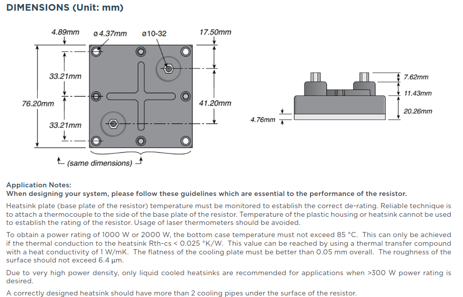
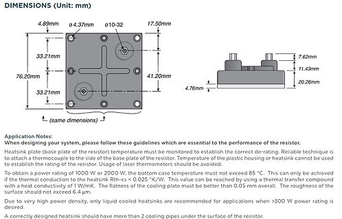
thermal conduction to the heatsink Rth-cs < 0.025 °K/W. This value can be reached by using a thermal transfer compound with a heat conductivity of 1 W/mK. The flatness of the cooling plate must be better than 0.05 mm overall. The roughness of the surface should not exceed 6.4 µm.
Due to very high power density
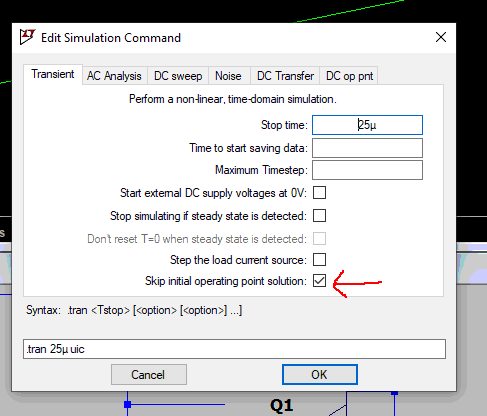
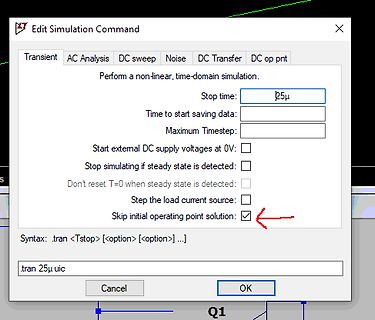
Edit Simulation Command
Transient AC Analysis DC sweep Noise DC Transfer DC op pnt
Perform a non-linear, time-domain simulation.
Stop time: 25µ
Time to start saving data:
Maximum Timestep:
Stop simulating if steady state is detected:
Don't reset T=0 when steady state is
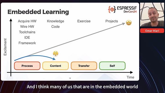
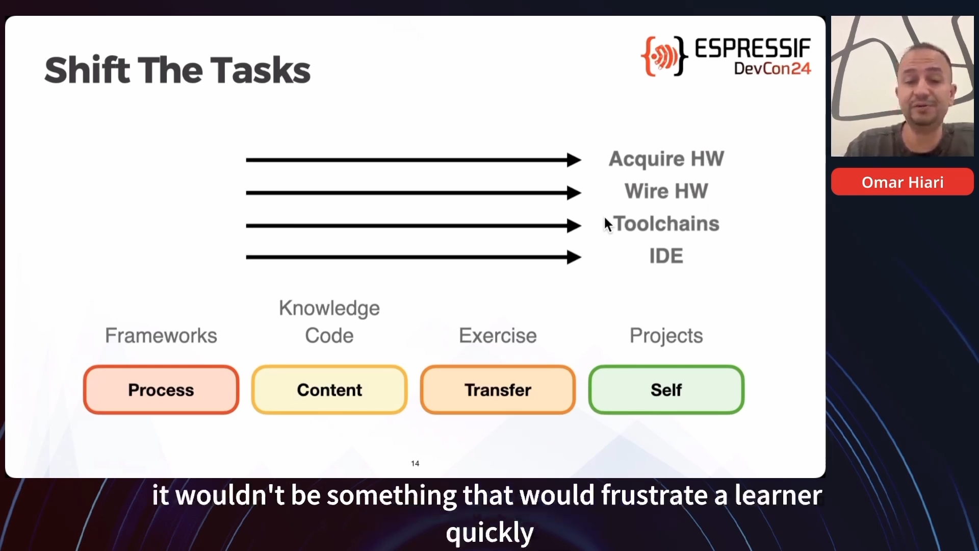
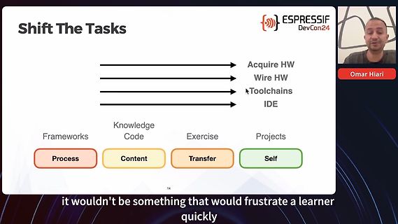
ESPRESSIF DevCon24
Acquire HW
Wire HW
Toolchains
IDE
Frameworks Process
Knowledge Code Content
Exercise Transfer
Projects Self
it wouldn't be something that would frustrate a learner quickly
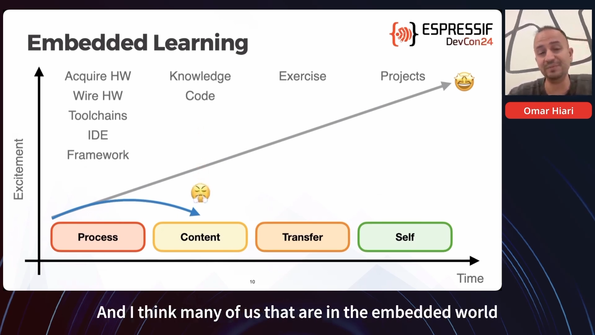
Framework
Knowledge
Code
Exercise
Projects
Espressif DevCon24
Omar Hiari
Excitement
Process
Content
Transfer
Self
Time
And i think many of us that are in the embeded world
Teil ähnlichen Antworten. https://unix.stackexchange.com/questions/195765/is-usb-to-usb-data-transfer-between-two-linux-oses-possible ... und hier noch ein Kabel für usb transfer unter linux https://www.thinkpenguin.com/gnu-linux/usb-30-data-transfer-cable-gnulinux-tpe-3trancbl https://www.thinkpenguin.com/gnu-linux/how-use-usb-data-transfer-cable-ubuntu
and Data Input any device that reads the data to be a receiver. The device that controls the data transfer is known During data input, the device samples Serial Data as the bus master, and the other as the slave de- (SDA) on the rising edge of Serial Clock (SCL). vice. A data transfer can only be initiated

 Bild
Bild
 Bild
Bild
 Bild
Bild
 Bild
Bild
 Bild
Bild
 Bild
Bild
 Bild
Bild
 Bild
Bild
 Bild
Bild
 Bild
Bild