PC bzw. RX/TX bool digitalRead (pin) sin (rad) cos (rad) tan (rad) } * mal / geteilt sqrt (x) pow (base, exponent) begin (long speed)//bis 921600Bit/s void loop ( ) { % Modulo (Rest der GZ-Division) digitalWrite (pin, [HIGH, LOW]) int constrain(x, minval, maxval) begin (speed, config) //Config z.B. //
PC bzw. RX/TX bool digitalRead (pin) sin (rad) cos (rad) tan (rad) } * mal / geteilt sqrt (x) pow (base, exponent) begin (long speed)//bis 921600Bit/s void loop ( ) { % Modulo (Rest der GZ-Division) digitalWrite (pin, [HIGH, LOW]) int constrain(x, minval, maxval) begin (speed, config) //Config z.B. //
ich hab hier öfters "s-video" gelesen. Ist dann aber schon etwas anderes, als "FBAS" oder "BAS".
Sigrid P. schrieb im Beitrag #7707757: > mit bas Anschluss an den > Monitor angeschlossen haben, und dieser laut aussage des Programierers > eine zu hohe Auflösung für den kleinen Röhrenmonitor habe.. Das BAS Signal ist auf 15,625 Khz genormt
Notepad die Beispiel Programme geöffnet. Bei MAKE ALL bekomme ich immer eine Fehlermeldung. RP6Base_LEDs.c:137: fatal error: opening dependency file .dep/RP6Base_LEDs.o.d: No such file or directory Woran kann das liegen? Freundliche Grüße Stephan
Allerdings funktioniert das Kompilieren trotzdem nicht. Ich bekomme folgende Ausgabe: > "c:\rp6base_examples\Example_01_LEDs\\make_all.bat" c:\RP6BASE_EXAMPLES\Example_01_LEDs>set LANG=C c:\RP6BASE_EXAMPLES\Example_01_LEDs>make all 0 [main] sh 19696 sync_with_child: child 1924(0x20C
gibt dort ein vereinfachtes Datenblatt auf dessen Homepages. https://www.digikey.be/en/products/base-product/renesas-electronics-corporation/20/IW3623/318916 Das Prinzipschaltbild und das interne Prinzipschaltbild sind dort zu finden: https://www.renesas.com/us/en/products/power-power-management
OX F VD(rms)=100V, AC50Hz S116S02 − − 10 TransferTurn-on time ton T (rms)=2A, Resistance loadF I =20mA ms charac- VD(rms)=200V, AC50Hz teristics S216S02 − − 10 T (rms)=2A, Resistance loadF I =20mA VD(rms)=100V, AC50Hz S116S02 − − 10 Turn-off time t T (rms)=2A, Resistance loadF I =20mA ms off VD(rms)
the ER● ● ● EC with ER GH housing and ER-AK, ER-AH or ER-AB with the ER EC fan insert. Air volume – base load 30 m³/h for continuous ope●ation ● ● ● Air volume of the base load and full load levels can be s●t ● ● Additional air volumes that can be set ● ●*** ● in base load: 20 m³/h, 40 m³/h, 60 m³/h or
Struktur geschoben werden, sonnst stimmt der Zugriff nicht mehr. Durch die Struktur die ab PA_BASE im Süeicher liegt weiß der Compiler dann, dass PMD auf Adresse PA_BASE + 0, OFFD auf PA_BASE + 32, DOUT auf PA_BASE + 64 liegt, usw.
Hannes J. schrieb im Beitrag #7701316: > MD auf Adresse PA_BASE + 0, OFFD auf PA_BASE + 32, DOUT auf > PA_BASE + 64 Nö, es sei denn man zählt Adressen in Bits statt in Bytes.
measurement is guaranteed by the accuracy of the HSE. The software can obtain the accurate RTC clock base by adjusting the 20 bit prescaler of the RTC, and obtain the accurate independent watchdog (IWDG) timeout time by calculation. The LSI calibration steps are as follows: 1. Turn on TIM5 and set channel
ordering information, kindly refer to Table 12. www.sensirion.com / D1 Version 6.4 – November 2023 20 / 24 10 Ordering Information Material Description Material Number Details Quantity (pcs) SHT40-AD1B-R2 3.000.465 base RH&T acc., 0x44 I2C addr. 2’500 SHT40-AD1B-R3 3.000.353 base RH&T acc., 0x44 I2C
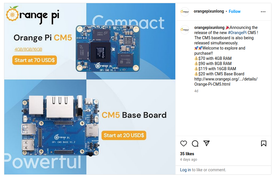
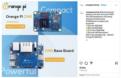
orange pi Compact Orange Pi CM5 4GB/8GB/16GB Start at 70 USD$ Rockchip orangepi CM5 V1.1 CM5 Base Board Start at 20 USD$ Powerful orangepixunlong Announcing the release of the new #OrangePi CM5 ! The CM5 baseboard is also being released simultaneously. Welcome to explore and purchase!! $70 with 4GB RAM $90 with 8GB RAM $119 with 16GB RAM $20 with CM5 Base Board http://www.orangepi.org/.../details/Orange-Pi-CM5.html 4d 35 likes 4 days ago
ordering information, kindly refer to Table 12. www.sensirion.com / D1 Version 6.4 – November 2023 20 / 24 10 Ordering Information Material Description Material Number Details Quantity (pcs) SHT40-AD1B-R2 3.000.465 base RH&T acc., 0x44 I2C addr. 2’500 SHT40-AD1B-R3 3.000.353 base RH&T acc., 0x44 I2C
Register anzeigen lasse, bekomme ich "14" angezeigt. Was ist dann dort eingestellt? Vorher wurde dort 20 angezeigt. Wenn ich das zum umrechnen in einen Rechner eingebe, dann bleibt das MSB immer 1. Erstmal wüsste ich gerne was diese "14" für ein Wert ist und kann man den auch binär ausgeben? Und weiter
den DS3231SN von Dallas haben, ruft Segor ganz entspannt 15.90EUR auf. Das ist auch bei BerryBase das gleiche: China-Ware auch ca. 5EUR, DS3231 mit Herkunftsnachweis ca. 15 - 20EUR. Ist halt leider das Risiko wenn man nicht beim Distributor kauft.
rating Tol. Pack-Code TCR Forming type R Value Special Power & Energy Computer & J = ±5% T = Tape - Base on52- Inner Taping UL = UL Version Peripherals (ammo pack) spec. dimension or YY = Standard 73- Inner Taping Automotive dimension ZB- Z version Historical VTM Part Nr.: CRF254 – 8 5 T 150R Precision
Collector-emitter VoltageBEV= 0) 32 45 V V CEO Collector-emitter VoltagB (I = 0) 32 45 V V EBO Emitter-base Voltage CI= 0) 7 V C Collector Current 200 mA I Base Current 50 mA B Ptot Total Power Dissipation atamb 25 ⋅C 0.39 mW at Tcase 45 ⋅C 1 W T stg Tj Storage and Junction Temperature – 65 to 200 ⋅C January
Augen wechselseitig nicht leiten bei -15V??? Ziel ist an den beiden Dioden zwischen den Drains +/- 20V zu haben. Funktioniert auch insoweit, dass die beiden LED wechselnd blinken.
Diese dinger hier, die "radar sensor 20W" nicht die PIR dinger: https://de.aliexpress.com/item/1005006853155930.html Funktion is excellent. Der dopplerradar erkennt bewegung 5m weit auch durch türen und wände und macht dann bei dunkelheit
by up to 1MHz. My theory: the low frequency doppler shift causes small changes in the transistor base bias. I used spice simulations to verify that small changes to transistor base bias causes changes in oscillation frequency. By running a few simulations I estimate that 1µV change in bias will change
...................................................................................................20 7-1.BEFORE PERFORMING SERVICE ......................................................................................... 20 7-2.LOAD TEST MODE .........................................................
scope at /home/christoph/Entwicklung/Modell/modelJulia.jl:15 [2] include(::Module, ::String) at ./Base.jl:377 [3] exec_options(::Base.JLOptions) at ./client.jl:288 [4] _start() at ./client.jl:484 in expression starting at /home/christoph/Entwicklung/Modell/modelJulia.jl:15 [/c] Hast Du einen
Ergebnis eine Spuleninduktivität von 4.2mH und bei 1KHz 3.2mH. Edit: Der Rotor stand bei ca. -20°
25A per channel Total harmonic distortion At any level up to rated power, into 4 or 8 ohms <0.05% (20Hz – 20kHz) Typically <0.005% at 1kHz Frequency response +-0.2dB (20Hz – 20 kHz) -1dB at 1Hz and 100kHz Residual hum and noise Referenced to full power -122dB, 20Hz – 20kHz, unweighted Voltage gain x
to 85 -40 to 85 -40 to 85 -40 to 85 -40 to 85 -40 to 85 -40 to 85 -40 to 85 -40 to 85 E e IP Class 20 20 20 20 20 20 20 20 20 s l n E Weight (kg) 0.27 0.34 0.28 0.32 0.31 0.31 0.26 0.26 0.43 Connectors (6.3 mm spades or purpose-built) spades spades spades spades spades spades spades spades spades Fan
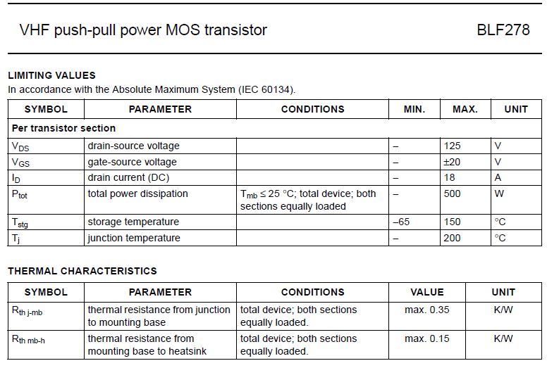
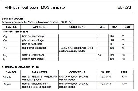
MIN. MAX. UNIT
Per transistor section
VDSS drain-source voltage - 125 V
VGSS gate-source voltage - ±20 V
ID drain current (DC) - 18 A
PTOT total power dissipation Tmb ≤ 25 °C; total device; both sections equally loaded - 500 W
Tstg storage temperature -65 150 °C
TJ junction temperature - 200 °C
THERMAL
130 - 147 An Ultra Low Cost HF SSB/CW Transceiver with 20W Output, an AGC HF Equipment Meter, S Meter and Audio Filter, Pt2 Denys Roussel, F6IWF 1996/3 148 - 156 Antenna Active Reception Antennas : Calculations and Experiments Part 2 Dipl Ing Detlef Burchard
Minimum time between reset-inactive and any master signal change. (1)Timings shown for oscillator base frequency of 20MHz (Fast mode). 2. Slave Reset On internal soft failures the Slave resets after 1 second or after an (error) frame is sent. On internal hard failures the Slave resets itself. In that
der negativen Halbwelle gibt es keine Begrenzung, die VAS liefert beliebig viel Strom, das kann der Q20 nicht ableiten.
negativen Halbwelle gibt es keine Begrenzung, die > VAS liefert beliebig viel Strom, das kann der Q20 nicht ableiten. Wenn ich dich richtig verstanden habe fließt der Strom im Fall von leitendem Q20 eben nicht durch die beiden unteren Mosfets Q24,Q23 sondern durch die VAS Mosfets Q16,Q17 die in dem
and fall times that depend on the transmitter’s peraturs is at a higher optical peak power limit (20 µW; control signal, the transmitter’s speed and possibly -17 dBm) compared with operation atTA=25° C. effects from the transmission link SFH551/1-1:maximallightpower • Pulse amplitude that depends on
ich mich dort über ca. 3 Stunden aufhielt, und das Gerät derweil von einer Kühlraumtemperatur von +20°C auf ca. 2°C runterkühlte und dann weiterlief, kam es (dank meiner Anwesenheit?) natürlich zu keinem Ausfall. Aber u.s.w., mal ein Blick auf die Seite 40 der Anleitung dort: https://static.ggmgastro.com/K%C3%BChlung/kuehlschrank/kgi%26tgi/KGI%20TGI%20Anleitung%20DE.pdf Auf dem rechten Bild erkenne ich, dass die Medium-Leitungen des Condensor aus Kupfer bestehen; am realen Gerät ist das nicht (mehr) erkennbar, war aber anzunehmen und
Memory The category is display-only which is determined by POST (Power On Self Test) of the BIOS. Base Memory The POST of the BIOS will determine the amount of base (or conventional) memory installed in the system. The value of the base memory is typically 512 K for systems with 512 K memory installed
Siemens_Consumer_IC_Data_Book.pdf#page=82 aber die sind teilweise digital. ein ELV-Bausatz damit: https://files2.elv.com/public/20/2040/204076/Internet/1982_19_07_dreiklanggong.pdf Lothar hat dazu auch etwas http://www.lothar-miller.de/s9y/archives/85-SAB0600.html
freq3 = 440; % A freq4 = 330; % E fmod = 1.4; % modulation freq relative to base amod = 2.5; % modulation amplitude decay = 1; % decay time [s] t = linspace(0,duration-1/fs,fs*duration); % cretae time vector env = exp(-t/decay); % decay envelope y = amp
limits of typical app write o x I/O behaviors during normal usage behaviors. Automated tools [2, m 20 d 32] are often unsuitable for testing apps with non-deterministic 0 behavior. Another issue is that gaming apps use custom libraries e ay o r x ej y o o ftd h e sp r y 2 s k r lr k i d d r k es n n
either 125 MHz, 62.5 MHz, 41.66 MHz, or 25 MHz clocks by setting the on-chip bus control register (0x20) for KSZ8851SNL system timing. These internal clocks are generated from an external 25 MHz crystal or oscillator. 3.2.4 SCRAMBLER/DE-SCRAMBLER (100BASE-TX ONLY) The purpose of the scrambler is to spread
Net-Ties und IPC-D-356-Daten umgeht. Bis einschließlich V19.x ließ sich da nix konfigurieren, seit V20 gibt es bei den Einstellungen die Option "Merge Net-Tie Nets - when enabled, if a design contains nets connected by Net-Tie components, these nets will report as distinguished single nets in the netlist
meiner Bords waren immer 2-Layer, wo es auch wie gewünscht funktionierte, weil ich mir damals vor 20+ Jahren keine vierlagigen Bords privat leisten konnte.
Guten Abend, ich habe in der Definition des SFP Standards auf Seite 20 und 21 die Pin Belegung gefunden. Nachdem ich diesen Artikel hier: https://www.computerbase.de/forum/threads/eigenes-modem-an-ftth-anschluss-via-sfp-gpon-modul.2061989/ gelesen habe, wollte ich
Art und Weise wie er angesteuert wird, nur die Pins, die sind eben nicht die selben wie im ComputerBase Artikel. Wo in diesem steht: USB UART Adapter ------------ SFP 20pins Molex connector 3.3V ------------- red -----------pin #15 und #16 TX --------------- orange --------pin #2 RX --------
Geht das nicht besser Sicher. > oder habe ich den falschen Regler erwischt? Zumindest das bas billigste aus Amazonien. Wer billig kauft, kauft 2 x.
geringe Differenz zwischen > Ein- und Ausgang. Von den 100% muss der Wandler in dem Fall ja nur 20% weg nehmen. 80% Wirkungsgrad bekommt er daher bereits geschenkt. Jetzt mus er nur noch 20% der Spannung mit 75% Wirkungsgrad loswerden, um insgesamt auf 95% Wirkungsgrad zu kommen. Zahlen schön-rechnen
Das sind Varianten des Prozessors, ich hab cl025. Wo ich jetzt zumindest das weiß, kann ich ja den 20ten Versuch starten. Ich verstehe immer noch nicht, warum - obwohl ich mich strikt an die von Johan beschriebene Inst-Prozedur gehalten hab - es immer noch daran scheitert, dass diese "Radioberry.ko"
die Radioberry.rbf etlich mal vorhanden ist, ist mir auf dem Raspi auch aufgefallen; ich fand etwa 20 davon. Wer weiß, was bei all den gescheiterten Versuchen so alles an Datenmüll auf dem Raspi entstanden ist, deshalb überlege ich, ob ich den noch mal neu aufsetze. Außerdem werd ich diese unhandliche
1.0 x 1.0 mm Component size to to to to to 18.7 x 18.7 mm 2 32 x 32 mm 2 13 x 13 mm 2 55 x 55 mm 2 20 x 20 mm 2 92 mm edge length Max. component height 6 mm 8.5 mm 8.5 mm 20 mm c 20 mm c Max. component weight 2 gr 5 gr 5 gr 25 gr 25 gr Placement force 2.4 - 5.0 N 2.4 - 5.0 N 2.4 - 5.0 N 1 - 10 N 1 -
epp.industrie.de/allgemein/recycling-von-smd-verpackungen/ https://www.newmatik.com/de/knowledge-base/KB-DE-00930/recycling-von-rollen-und-trays-fur-smd-bauteile dort hattest du schon mal angefragt?
Kunsststoffrecycler, ansonsten gehts halt in die Müllverbrennung: https://www.europages.de/unternehmen/aufbereitung%20und%20recycling%20von%20abf%C3%A4llen.html > Ich habe einen Kunststoffrecycler gefragt, der würde Sie nur nehmen, > wenn keine Etiketten mehr drauf sind. Dann testhalber mal in den geschirrspüler
permanent damage to the device may occur. Parameter Symbol Value Units DC supply voltage range (pin 2, I= 20mA max) VCC -0.3 to 18 V CC Continuous DC supply current at V pin (V = 15V) I 20 mA CC CC CC V input (pin 8, I ≤ 10mA) -0.7 to 4.0 V SENSE Vsense I input (pin 6) -0.3 to 4.0 V SENSE ESD rating per JEDEC
dem Schreibtisch mit 1m > Klingeldraht? Hängt vom Chipsatz ab. Meine Erfahrungen liegen schon 20 Jahre zurück. Da gab es sicher jede Menge Verbesserungen.
einstellbar) SHRM-08-s ATM-Modemkarte - Modemkarte für 4-Draht Anwendungen inkl. 1 Port Ethernet 10/100Base Tx Für mich liest sich das Problem damit erklärt an der Technik dieser spez. Baugruppe. Der Hersteller oder eher Vertrieb gibt aber wohl keinen wirklichen Support dazu.
Serial Rx read only port Damals habe ich das so gemacht // PIO 8255 Special I/O __sfr __at 0x20 PIO8255_PORT_A; __sfr __at 0x21 PIO8255_PORT_B; __sfr __at 0x22 PIO8255_PORT_C; __sfr __at 0x23 PIO8255_CNTRL; Dahinter steckten 4 Register des 8255 am I/O Bus des Z80, die mit speziellen Werten
The principal entry point to the FDOS is at location BOOT+0005H (normally 0005H) where a jump to BASE is found. As mentioned above, access to the FDOS functions is accomplished by passing a function number and information address through the primary point at location BOOT+0005H Danke, das reicht
Symbol Min Typical Max Units Supply Voltage VCC 3.15 3.3 3.46 Vdc Supply Voltage Ripples VCC_PP 2 % 100Base-TX Active CC 225 270 mA (Evolution) 100Base-TX Active (Linux) I 200 270 mA CC 100Base-TX Idle (Evolution) CC 215 mA 100Base-TX Idle (Linux) CC 175 mA 10Base-T Active (Evolution) I 145 250 mA CC 10Base-T
05 1.00E+06 1.00E+07 1.00E+08 1.00E+09 1.00E+10 100000 1000000 10000000 100000000 1E+09 1E+10 –10 -20 –20 –30 -40 –40 B B -60 d –50 d –60 -80 –70 –80 -100 –90 –100 -120 Frequency (Hz) Frequency (Hz) C001 C002 Figure 3. XTALK Port A Figure 4. XTALK Port B 0 0 100000 1000000 10000000 100000000 1E+09 1E+10 100000 1000000 10000000 100000000 1E+09 1E+10 -10 -20 -20 -30 -40 -40 B -50 B -60 d d -60 -80 -70 -80 -100 -90 -100 -120 Frequency (Hz) Frequency (Hz) C003 C004 Figure 5. Off-State Isolation (OISO) for Port A Figure 6. Off-State Isolation (OISO) for Port

 Bild
 Bild
 Bild