there is a vibration source nearby Protect the servo amplifier from vibration by installing it on a base with a shock absorber. If there is a heat generator nearby If the ambient temperature may increase due to convection or radiation, make sure the temperature near the servo amplifier does not exceed
material (3) (4/5) (6) SN74LV367AD ACTIVE SOIC D 16 40 RoHS & Green NIPDAU Level-1-260C-UNLIM -40 to 85 LV367A SN74LV367ADE4 ACTIVE SOIC D 16 40 RoHS & Green NIPDAU Level-1-260C-UNLIM -40 to 85 LV367A SN74LV367ADGVR ACTIVE TVSOP DGV 16 2000 RoHS & Green NIPDAU Level-1-260C-UNLIM -40 to 85 LV367A SN74LV367ADR ACTIVE SOIC D 16 2500 RoHS & Green NIPDAU Level-1-260C-UNLIM -40 to 85 LV367A SN74LV367ANSR ACTIVE SO NS 16 2000 RoHS & Green NIPDAU Level-1-260C-UNLIM -40 to 85 74LV367A SN74LV367APWR ACTIVE TSSOP PW 16 2000 RoHS & Green NIPDAU Level-1-260C-UNLIM -40 to 85 LV367A SN74LV367APWRG4
Case temperature T c 150 Storage temperature Tstg -40 ~ 150 Isolation between terminal and copper base (*1) V isol AC: 1min. 4000 Vrms voltage between thermistor and others (*2) Mounting torque of screws to heatsink (*3) M s M5 6.0 Mounting torque of screws to main terminals (*3) M M8 10.0 N·m Mounting
1.144 V BG CC A V =1.7V to 5.5V at Internal 1.1V reference voltage CC 1.067 1.1 1.133 V TA=-40°C to 85°C VCC=2.3V to 5.5V at VREF Internal 2.2V reference voltage T =-40°C to 85°C 2.134 2.2 2.266 V A Internal 4.096V reference voltage VCC=4.2V to 5.5V at 3.932 4.096 4.260 V TA=-40°C to 85°C VCC = 1.8V 2000
coefficient oscillator. termsofa / ⋅CLSB,yieldingthefollowing9–bitformat: 2 The counter is preset with a base count that corre- MSB LSB spondsto–55⋅C.Ifthecounterreacheszerobeforethe 1 1 1 0 0 1 1 1 0 gate period is over, the temperature register, which is also preset to the –55⋅C value, is incremented, indicat
36.7 mm (1.445 in) x 19.05mm(0.75in)x18.67mm(0.735in) NETWORK INTERFACE- WIRED PHYSICALLAYER 10/100Base-T DATA RATE 10/100 Mbps (auto-sensing) MODE Full- or half-duplex (auto-sensing) CONNECTOR RJ-45 w/ magnetics POE POWERPASS-THROUGH 802.3af compliant (Mid-andEnd-span) ENVIRONMENTAL OPERATINGTEMPERATURE -40° C to 75° C (-40° F to167°F)-40°Cto85°C(-40°Fto185°F)withexternalthermalpad* STORAGETEMPERATURE -50° C to 125° C (-58° Fto257°F) RELATIVEHUMIDITY 5% to 90% (non-condensing) POWER REQUIREMENTS(3.3 VDC) MAXIMUM 450 mA (1.485 W) 346 mA (1.14
-40 C to +85C° Industrial GD32E230G8U6 64 QFN28 Green -40 C to +85C° Industrial GD32E230G6U6 32 QFN28 Green -40 C to +85C° GD32E230G4U6 16 QFN28 Green Industrial -40 C to +85C° Industrial GD32E230F8V6 64 LGA20 Green -40 C to +85C° Industrial GD32E230F6V6 32 LGA20 Green -40 C to +85C° GD32E230F4V6 16 LGA20 Green Industrial -40 C to +85C° Industrial GD32E230F8P6 64 TSSOP20 Green -40 C to +85C° Industrial GD32E230F6P6 32 TSSOP20
1.144 V BG CC A V =1.7V to 5.5V at Internal 1.1V reference voltage CC 1.067 1.1 1.133 V TA=-40°C to 85°C VCC=2.3V to 5.5V at VREF Internal 2.2V reference voltage T =-40°C to 85°C 2.134 2.2 2.266 V A Internal 4.096V reference voltage VCC=4.2V to 5.5V at 3.932 4.096 4.260 V TA=-40°C to 85°C VCC = 1.8V 2000
specified, all measurements are made at a temperature of 15° to 35° C, a relative humidity of 25% to 85%, and an atmospheric pressure of 86 to 106 kPa and all S- parameters are normalized with an 85 Ω differential impedance. 3.7.1 Raw Cable (Informative) Informative raw cable electrical performance targets
16 colors 70 T, G, B 640 x 350 16 colors 70 T, G, B G, B 640 x 480 16 colors 60 256 colors 60, 75, 85 G, B, L 64 K colors 60, 75, 85 G, B, L 16 M colors 60, 75, 85 G, B, L 720 x 400 16 colors 70 T, B 800 x 600 256 colors 60, 75, 85 G, B, L 64 K colors 60, 75, 85 G, B, L 16 M colors 60, 75, 85 G, B, L
would have an efficiency of NathanSokal@compuserve.com design equations did not include the about 85% (losses = 15% of input Jan/Feb 2001 9 power) if changed to Class E (35%/15% will, unavoidably, be appreciable frac- The timing requirements of 3 and 4 are = 2.3). Class-E amplifiers can be de- tions
-Q2 emitters. The low Q2 The bottom trace is the drain voltage (10.1MHz) configuration. Since the base voltage emitter-collectorresistance,whichisin (Vd) at 5v/div. The peak-to-peak 99nS is an 8v square wave, the transistors voltage is about 25v, the 2Vcc (or s: 20nS/ are driven nearly into saturation
saturation, and the point of maximum the automotive industry as turn-signal collector current. The base voltage First Published in the journal "QRPp" blinkers and headlight dimmers to requiredtosaturatethetransistorvaries replace the expensive electro- Part 1 is a tutorial for using switching MOSFET's
software tool for evaluation. The TMC2209 evaluation board system consists of three parts: STARTRAMPE (base board), ESELSBRÜCKE (connector board with several test points and stand-alone settings), and TMC2209-EVAL. O RDER C ODES 2 Order code Description Size [mm ] TMC2209-LA Stepper Motor Driver/Controller
falls rapidly while the output voltage decrease slowly. The capacitance discharges by means of the Base-tage Emitter junction of the series pass transistor in the regulator. If the energy is sufficiently high, the transistor may be destroyed. The external diode by-passes the current from the IC to ground
PNP Transistoren in DFN1110D-3. • BAT32LS-Q und BAT42LS-Q Schottky-Dioden in DFN1006BD-2 • BAS21LS-Q Schaltdiode in DFN1006BD-2. • PDTA143/114/124/144EQB-Q - 50 V 100 mA PNP Resistor-Equipped Transistors (RET) in DFN1110D-3. • 2N7002KQB - 60 V N-Kanal Trench MOSFET und BSS84AKQB -
Strombelastbarkeit von jeweils 0,5 A bieten. Der Betriebstemperaturbereich liegt zwischen -55 und 85 °C; die Board-to-Board-Stackhöhe beträgt 8 mm. [/c] 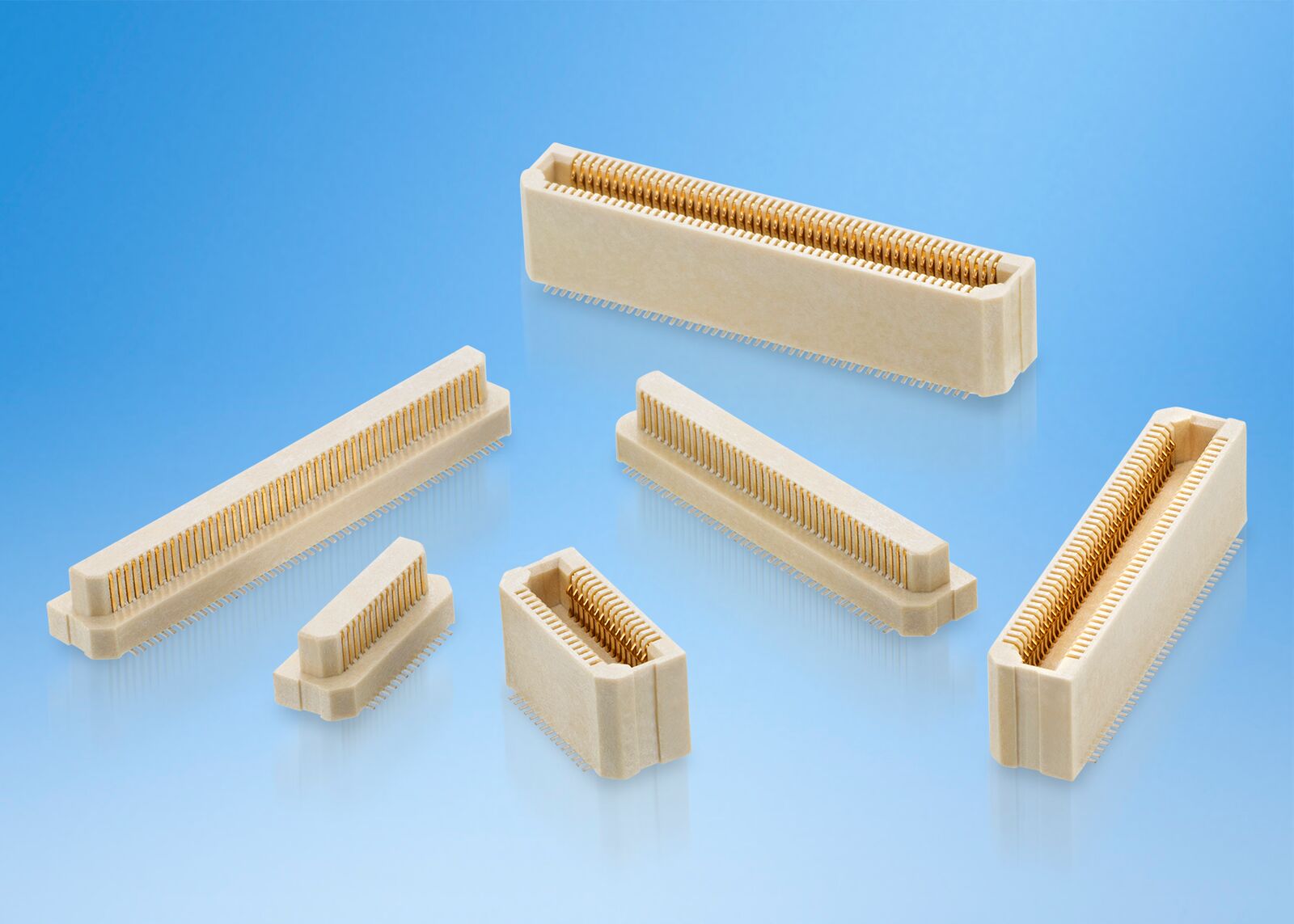 (Bildquelle: Harwin) Interessant ist, dass die Bauteile für die Verarbeitung per Pick&Place-Maschine optimiert
respecVDD, VCx to VSS -0.3 36 V PIN voltage range respecCO -0.3 VDD+0.3 V Operation Temperature -30 85 °C Storage Temperature Tstg -40 125 °C Caution: Stresses beyond "Absolute Maximum Ratings" condition may cause permanent damage to the device. These are stress ratings only and functional operation of
V EB= 6 V,CI = 0 100 nA h V = 1 V, I = 5 mA 45 FE1 CE C hFE2 DC Current Gain V CE= 1 V,CI = 100 mA 85 300 hFE3 V CE= 1 V,CI = 800 mA 40 VCE (sat) Collector-Emitter Saturation VoltIC= 800 mA, B = 80 mA 0.5 V VBE (sat) Base-Emitter Saturation Voltage IC= 800 mA, B = 80 mA 1.2 V V (on) Base-Emitter On Voltage
/ Cursor u w I s j h 1 Save / Recall i2. : 1 . j . 2 Reference Memories i * J . |: I f Dual Time Base « 1 ] . I A3 V v A 4 :| * f * 8 { a I Component Tester 1 I 1kHz/1MHz Calibrator RS232 Interface Analog: Digital: ■ 2 x DC to 150MHz, 2 x 1mV-50V/div ■ Refresh, Single, Roll-, Envelope-, Average-,XY-Mode ■ Time Base A with Trig. DC to 250MHz ■ Max. Sampling Rate 200MSa/s, Storage 2x2048x8 bit ■ Time Base B with 2ndTrig. to 250MHz ■ Time Base A: 100s - 50ns/div., B: 20ms - 50ns/div. ■ Trig. DC to 250MHz, TV Sync
The mirror-pair transistors also function as a differential-to- single-ended converter to provide base drive to the second- Terminal 8 can be used both for phase compensation and to stage bipolar transistor (Q ). Offset nulling, when desired, can strobe the output stage into quiescence. When Terminal
I O 0 2.7 V 4 8 1.65 V 2 4 5.5 V 0.2 2 CC VI= GND (3,OI = 0, -40 ℃ ≤ A ≤ 3.6 V 0.1 2 μA Low inputs 85 ℃ 2.7 V 0.1 1 1.65 V 0.1 1 5.5 V 0.2 2 Standby mode VI= V CC,OI = 0, -40 ℃ ≤ A ≤ 3.6 V 0.1 2 High inputs 85 ℃ 2.7 V 0.1 1 1.65 V 0.1 1 3.6 V 1 2 Low and High VI= V CCor GND, IO= 0, 85 ℃ < Inputs T ≤
NRND TVSOP DGV 24 TBD Call TI Call TI -40 to 85 PCA9548ADGVR ACTIVE TVSOP DGV 24 2000 RoHS & Green NIPDAU Level-1-260C-UNLIM -40 to 85 PD548A PCA9548ADW ACTIVE SOIC DW 24 25 RoHS & Green NIPDAU Level-1-260C-UNLIM -40 to 85 PCA9548A PCA9548ADWG4 ACTIVE SOIC DW 24 25 RoHS & Green NIPDAU Level-1-260C-UNLIM -40 to 85 PCA9548A PCA9548ADWR ACTIVE SOIC DW 24 2000 RoHS & Green NIPDAU Level-1-260C-UNLIM -40 to 85 PCA9548A PCA9548APWR ACTIVE TSSOP PW 24 2000 RoHS & Green NIPDAU Level-1-260C-UNLIM -40 to 85 PD548A PCA9548APWRG4
preceding the number. Table 1-2 lists the four bases supported by ABEL-HDL and their accompanying symbols. The base symbols can be upper- or lowercase. Table 1-2. Number Representation in Different Bases Base Name Base Symbol Binary 2 ^b Octal 8 ^o Decimal
single-ended supplies, the driver outputs are grounded. In conventional push-pull bipolar designs, forward base drive is The V terminal is switched to ground by the totem-pole controlled byR1-R3.Rapidturn-offtimesforthepowerdevices C source transistors on alternate oscillator cycles. are achieved with speed-up
0.4 to 6 GHz application, the single 5.0V supply, the LNA Applications LNA focus is Cellular/PCS base typically draws 53 mA. This • Cellular/PCS base station radio stations. alignment results in an Input card LNA Intercept Point of 17.5 dBm. • High dynamic range amplifier for To attain NF min condition
is not actually real. The parasitic capacitances in BJTs are mainly due to the two P{N junctions (base-emitter and base-collector), the depletion-layer capacitances of those P{N junctions being modeled by the same equations and analogous parameters as in the case of diodes. The e®ects of the parasitic
Characteristics Collector-emitter breakdown voltage V(BR)CEO 50 - - V I = 100 µA, I = 0 C B Collector-base breakdown voltage V(BR)CBO 50 - - IC= 10 µA, IE= 0 Collector-base cutoff current ICBO - - 100 nA VCB = 40 V, E = 0 Emitter-base cutoff current IEBO - - 350 µA VEB = 10 V, C = 0 DC current gain2) h 50
SCLK SSC Master Clock Outp./Slave Cl. Inp. 81 O P3.15 CLKOUT System Clock Output (=CPU Clock) P4.0 - 85 - 92 I/O Port 4 is an 8-bit bidirectional I/O port. It is bit-wise P4.7 programmable for input or output via direction bits. For a pin configured as input, the output driver is put into high- impedance
#7036955: > sagst- zu schwach mit ihren 1500W. Vielleicht einfach mal etwas Pfunde abbauen. Mit 85kg statt 150kg klappt das auch mit dieser Leistung. 😁😁😁
#7036955: >> sagst- zu schwach mit ihren 1500W. > Vielleicht einfach mal etwas Pfunde abbauen. > Mit 85kg statt 150kg klappt das auch mit dieser Leistung. Nichts klappt mit dieser Leistung. Mein mit eigener Messtechnik bestücktes Pedelec wiegt 20kg (plus 70kg Fahrer) und genehmigt sich 750W, wenn es
Reference Manufacturing* PbFree Temperature Range Package MIC2981BN** MIC2981/82BN MIC2981/82YN –40ºC to +85ºC 18-pin DIP MIC2982BN** MIC2981/82BN MIC2981/82YN –40ºC to +85ºC 18-pin DIP MIC2981BWM** MIC2981/82BWM MIC2981/82YWM –40ºC to +85ºC 18-pin wide SOP MIC2982BWM** MIC2981/82BWM MIC2981/82YWM –40ºC to +85ºC 18-pin wide SOP * Order entry P/N. **Orders for MIC2981BN or MIC2982BN will be filled with dual-marked MIC2981/82BN. **Orders for MIC2981YN or MIC2982YN will be filled with dual-marked MIC2981/82YN
2 Big-Endian Protocol ID 2 Big-Endian Length 2 Big-Endian Unit ID 1 Modbus Data Function Code 1 0x85 Error Data Code 1 0x01 5.2.5 Write Multiple Microinverters Status ü Command sending format Name Length Value Remark Header Transaction ID 2 Big-Endian Protocol ID 2 Big-Endian Length 2 Big-Endian Unit
ich habe gefunden diese : https://www.effectrode.com/knowledge-base/binson-echorec-schematic/ Leider ist mein English , so gut wie mein Deutsch und ich verstehe wenig von der Funktionsbeschreibung, kann man Diesen verwenden lg grosi
MD85b schrieb im Beitrag #7042112: > grossi, Wolfgang, soso, oder doch nicht etwa Reinhard? > > grins... Was hast Du denn herausgefunden? Immer raus damit... ;) grossi schrieb im Beitrag #7042570
8 2500 RoHS & Green NIPDAU Level-1-260C-UNLIM -40 to 85 TL072I TL072IDRE4 ACTIVE SOIC D 8 2500 RoHS & Green NIPDAU Level-1-260C-UNLIM -40 to 85 TL072I TL072IDRG4 ACTIVE SOIC D 8 2500 RoHS & Green NIPDAU Level-1-260C-UNLIM -40 to 85 TL072I TL072IP ACTIVE PDIP
Das scheint ein ZX85 Board zu sein, vom Computerclub Jena entwickelt: https://www.robotrontechnik.de/html/computer/bausaetze.htm Ziemlich weit unten. Dein Board unterscheidet sich dadurch, das bei dir ein zweites EPROM
Leitung geht zu einem HF-Stecker. Da ist mir > nicht klar was da ausgegeben wird Wird wohl Video (BAS Signal) sein.
