-
PDF
AN1819.pdf
compensate for the thermal characteristics of MOSFETs. Some may incorporate some form of shutdown mechanism when a thermal limit is reached: standby switching, and/or thermally activated fan speed control. Figure 3 · Temperature-compensated Bias Supply
in „Stackpole Ferrit Kerne für RF Verstärker“ · HF, Funk und Felder ·
-
PDF
fm600tu-07a_e.pdf
MITSUBISHI <MOSFET MODULE> FM600TU-07A HIGH POWER SWITCHING USE INSULATED PACKAGE FM600TU-07A ● ID(rms) .......................................................300A ● V DSS.............................................
in „Wechselrichter mit MOSFET Endstufe“ · Analoge Elektronik und Schaltungstechnik ·
-
PDF
ssr2n60a.pdf
Advanced Power MOSFET SSR/U2N60A FEATURES BV DSS = 600 V Avalanche Rugged Technology Rugged Gate Oxide Technology R DS(on) = 5 Ω Lower Input Capacitance I = 1.8 A Improved Gate Charge D Extended Safe Operating Area D-PAK
in „Ersatz für SSR2N60A“ · Analoge Elektronik und Schaltungstechnik ·
-
PDF
HKT05N10-_5N10_-.pdf
HKT05N10 HIGH VOLTAGE MOSFET (N-CHANNEL) FEATURES Low on-resistance:VDS100V,R DS(ON)115mΩ@V =10GSI =3A D Low Input Capacitance Fast Switching Speed Low Input/Output Leakage Surface Mount device MECHANICAL DATA SOT-23
in „Unbekanntes SMD Bauelement 5N10“ · Analoge Elektronik und Schaltungstechnik ·
-
 Bild
Marktübersicht zu Lieferzeiten und Preisen von Halbleitern
Devices 18-34 Sensors 22-46 Broadcom RF Devices 18-26 onsemi Bi-polar Power 14-24 IGBT 16-34 Power MOSFETs 16-34 Rectifiers 15-27 Small Signal 14-27 TVS/Protection 14-26 Zener Diodes 14-25 Infineon Bi-polar Power 9-12 IGBT 15-46 Power MOSFETs 15-41 Rectifiers 19-36 RF Devices 13-28 Sensors 18-42 Small Signal 12-26 Thyristors 20-36 ST Bi-polar Power 16-20 IGBT 18-37 Power MOSFETs 18-30 Rectifiers 19-34 Small Signal 18-27 Thyristors 18-28 TVS/Protection 16-28 nexperia Bi-polar Power n/a Power MOSFETs n/a Rectifiers n/a Small Signal n/a TVS/Protection n/a Zener Diodes n/a
in „Nexperia-Leadtimes steigen, Raspberry Pi-Buchapp mit Kontensystem uvam“ · Mikrocontroller und Digitale Elektronik · · Screenshots

-
PDF
linkswitch-hp_family_datasheet-844868.pdf
jittering reduces EMI filter cost • Fully integrated soft-start for minimum start-up stress • 725 V MOSFET simplifies meeting derating requirements Exposed (LNK677x) Pad Exposed • 650 V MOSFET for lowest system cost (LNK676x/LNK666x) Pad • Fast transient response family option (LNK666x) Extensive Protection
in „Fujitsu B27T-7 TFT Monitor Netzteil defekt Bauteil 715G6503-P01-001-0010“ · Analoge Elektronik und Schaltungstechnik ·
-
 Bild
Schaltplan eines Operationsverstärkers mit SPICE-Fehlermeldung
Circuit: Z:\home\ales\LTspice\TEST.asc Instance "mu1:4": Length shorter than recommended for a level 2 MOSFET. Instance "mu1:3": Length shorter than recommended for a level 2 MOSFET. Instance "mu1:2": Length shorter than recommended for a level 2 MOSFET. Instance "mu1:1": Length shorter than recommended for a level 2 MOSFET. Direct Newton iteration for .op point succeeded. Date: Mon Jul 29 17:51:30 2024 Total elapsed time: 0.1333 seconds. tnom = 27 temp = 27 method = modified trap toller = 2696 traniter = 2685 transpoints
in „LTspice AD8657“ · Analoge Elektronik und Schaltungstechnik · · Screenshots
-
PDF
2003161835_ZILLTEK-ZTP7192MS_C481285.pdf
to 15V rectified, step-down, switch-mode converter with ● Output current up to 2A internal power MOSFETs. It offers a very compact ● Integrated 80mΩ/45mΩ power MOSFET switches solution to achieve a2A continuous output current over ● Shutdown current 3μA typical a wide input supply range, with excellent
in „Ruhe-Stromaufnahme MP2315 Ali-Board zu hoch“ · Analoge Elektronik und Schaltungstechnik ·
-
PDF
OB2502.PDF
Connected to resistor 3 FB I divider from auxiliary winding reflecting output voltage. 4 CS I Power MOSFET source 5/6/7/8 Drain O Drain of internal power MOSFET ©On-Bright Electronics Confidential Datasheet OB_DOC_DS_2502xA2 - 3 - OB2502x High Precision CC/CV Primary-Side Power Switch BLOCK DIAGRAM ©On-Bright
in „SNT Gartenbeleuchtung defekt, pulst aber“ · Analoge Elektronik und Schaltungstechnik ·
-
PDF
171050601.pdf
is carried out during the off-time by monitoring the current in the synchronous MOSFET. Referring to the Functional Block Diagram, when the top MOSFET is turned off, the inductor current flows through the load, the PGND pin and the internal synchronous MOSFET. If this current exceeds
in „Stromverbrauch eines Abwärtswandlers“ · Analoge Elektronik und Schaltungstechnik ·
-
PDF
171050601.pdf
is carried out during the off-time by monitoring the current in the synchronous MOSFET. Referring to the Functional Block Diagram, when the top MOSFET is turned off, the inductor current flows through the load, the PGND pin and the internal synchronous MOSFET. If this current exceeds
in „Berechnung der Ausgangskapazität“ · Analoge Elektronik und Schaltungstechnik ·
-
PDF
MRF175GV.pdf
MOTOROLA Order this document SEMICONDUCTOR TECHNICAL DATA by MRF175GU/D The RF MOSFET Line RF Power MRF175GU Field-Effect Transistors MRF175GV N–Channel Enhancement–Mode Designed for broadband commercial and military applications using push pull circuits at frequencies to 500 MHz. The
in „Dimensionierung eines Kühlkörpers für HF-Modul“ · HF, Funk und Felder ·
-
Datei
Motor1.c
/////// //////////////////////////////////////////////////// void rechtskom () { // Für die High-Mosfets wird das Dutycycle auf duty für high und auf 0 für Low eingestellt (PWM nur für High MosFets) if ( PINB & (1<<PINB0) ) { if ( !(PINB & (1<<PINB1))) { w1=duty; //stellt den Wert duty als duty cycle
in „zwei if-Anweisungeg funktionieren nicht zusammen“ · Mikrocontroller und Digitale Elektronik ·
-
PDF
LT3800.pdf
compensation waveform is calibrated at an 80% 3800 AI03 3800fc 15 LT3800 APPLICATIONS INFORMATION Power MOSFET Selection The R required for a given conduction loss can be DS(ON) External N-channel MOSFET switches are used with the calculated using the relation: LT3800. The positive gate-source drive voltage
in „LT3800 Frage“ · Analoge Elektronik und Schaltungstechnik ·
-
PDF
OZ965.pdf
sufficient time for the Power is transferred to the transformer primary lamp to ignite. by the N-MOSFET, driven by the MOSFET gate driver out of pin NDR. The P-MOSFET resets the primary field, driven by pin PDR. The usual For system reliability there are several circuit design results in approximately
in „Background-Beleuchtung für TFT-Display“ · Mikrocontroller und Digitale Elektronik ·
-
PDF
Servicemanual-Lorch-IT-ESAB-Aristotig.pdf
inputs from high voltages, and the driver stages from pulse overload in case of faulty MOSFETs. The resistor (b) provides 1 kΩ for each MOSFET group. The gate series resistors (c) have a value of 8.2 Ω for each MOSFET. - 25 - A1-8 MAINS SWITCH MONITORING a1-8.pcx To ensure a defined ON/OFF
in „Schaltplan EWM TRSQW2 für Merkle Insquare 250W 350W, ESS SquareARC 351 WIG-Schweissgeräte“ · Projekte & Code ·
-
PDF
BTT_SKR_V1.4-SCH.pdf
GND GND 3 4 GND 5 RN5 4 5 6 TXD3 Y-DIR 6 3 YDIR R43 U6 DC3.3V 7 8 Y-STP 7 2 YSTP HE0_PWM 1 8 HBED_MOSFET C35 Y-EN 8 1 YEN MOS 10K HE0_PWM 2 9 HB_PWM 22UF 10V R44 HE0_MOSFET 3 10 GND GND 100R 【 Y 】 2 E1 D S GND HE1_PWM 4 11 FAN_MOSFET E1 1 VBB D6 10K HE1_PWM 5 12 FAN_PWM +5V GND SD-Card 2 E0 SDDET Q1 HE1_MOSFET 6 13 0 D7 E0 1 G HB_PWM R45 7 14 1 1 SDDET Motor Driver DC3.3V HE1_MOSFET 10K 9 P0.27 R46 DC3.3V VBB WSF3085 MC74HCT125ADTR2G R47 C37 TFT D D DAT2 1 C38 10K 0.1UF 5V G G CD DAT3 2 0.8-MISO1 1K R51
in „Induktiven Sensor (6-36V) an Microcontroller/Mainboard anschließen“ · Mikrocontroller und Digitale Elektronik ·
-
PDF
BTT_SKR_V1.4SCH.pdf
GND GND 3 4 GND 5 RN5 4 5 6 TXD3 Y-DIR 6 3 YDIR R43 U6 DC3.3V 7 8 Y-STP 7 2 YSTP HE0_PWM 1 8 HBED_MOSFET C35 Y-EN 8 1 YEN MOS 10K HE0_PWM 2 9 HB_PWM 22UF 10V R44 HE0_MOSFET 3 10 GND GND 100R 【 Y 】 2 E1 D S GND HE1_PWM 4 11 FAN_MOSFET E1 1 VBB D6 10K HE1_PWM 5 12 FAN_PWM +5V GND SD-Card 2 E0 SDDET Q1 HE1_MOSFET 6 13 0 D7 E0 1 G HB_PWM R45 7 14 1 1 SDDET Motor Driver DC3.3V HE1_MOSFET 10K 9 P0.27 R46 DC3.3V VBB WSF3085 MC74HCT125ADTR2G R47 C37 TFT D D DAT2 1 C38 10K 0.1UF 5V G G CD DAT3 2 0.8-MISO1 1K R51
in „3D-Drucker, Mainboard-Lüfteranschluss erweitern“ · Mikrocontroller und Digitale Elektronik ·
-
PDF
top247.pdf
DRAIN pin 4.8 V.At 4.8 V, auto-restart is activated which turns the output during start-up, the MOSFET is initially off, and the MOSFET off and puts the control circuitry in a low current CONTROL pin capacitor is charged through a switched high standby mode. The high-voltage current source turns on
in „Hilfe bei Reparatur SNT Laderegler“ · Analoge Elektronik und Schaltungstechnik ·
-
Datei
ADWandler.txt
PB2 / ADC 1 | ;| Batterie an PB4 / ADC 2 | ;| Messung an PB3 / ADC 3 | ;| Status LED an PB0 | ;| MOSFET an PB1 | ;| RESET an PB5 | ;| Referenzspannug VCC (5V) | ;| Masse GND (0V) | ;| | ;|Prozessor: | ;| ATTINY 13-20 DIP 3,6864 MHz | ;| | ;|Sprache: | ;| Assembler | ;| | ;|Datum: | ;| 16.04.2019 | ;|
in „AVR Attiny13 Assembler AD Wandler“ · Mikrocontroller und Digitale Elektronik ·
-
PDF
HF500-30.pdf
Line Compensation The Future of Analog IC Technology DESCRIPTION FEATURES 700V/1.4Ω Integrated MOSFET The HF500-30 is a fixed-frequency, current- mode regulator with built-in slope compensation. Fixed-Frequency, Current-Mode Control The HF500-30 combines a 700V MOSFET and Operation with Built-In
in „Marking Code Hilfe“ · Mikrocontroller und Digitale Elektronik ·
-
PDF
l6599.pdf
reason is that there is an internally fixed dead-time T , inserted between the turn-OFF of either D MOSFET and the turn-ON of the other one, where both MOSFETs are OFF. This dead- time is essential in order for the converter to work correctly: it will ensure soft-switching and enable high-frequency operation
in „Hilfe bei der Reparatur eines Schaltnetzteiles erbeten“ · Analoge Elektronik und Schaltungstechnik ·
-
 Bild
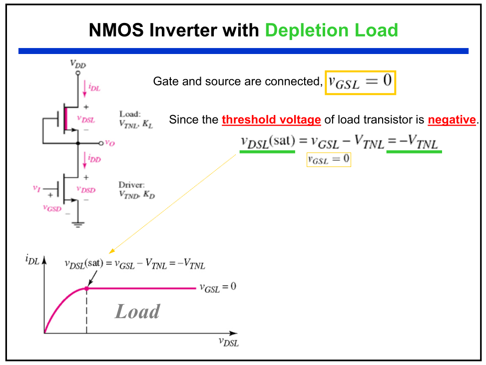
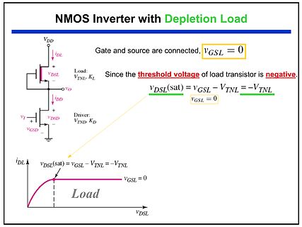
NMOS Inverter mit Depletion Load Erklärung
NMOS Inverter with Depletion Load VDD iDL + vDSL Load: VTNL, KL Gate and source are connected, vGSL = 0 Since the threshold voltage of load transistor is negative. vDSL(sat) = vGSL - VTNL = -VTNL vGSL = 0 vi + vDSD Driver: VTND, KD - VDD iDL vDSL(sat) = vGSL - VTNL = -VTNL vGSL = 0 Load vDSL
in „Schaltung mit 2 N-Kanal Mosfet“ · Analoge Elektronik und Schaltungstechnik · · Diagramme
-
 Bild
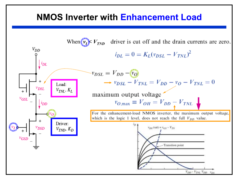
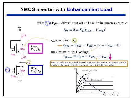
NMOS Inverter mit Enhancement Load Schaltplan und Kennlinie
NMOS Inverter with Enhancement Load When vI < VTND driver is cut off and the drain currents are zero. iDL = 0 = KL(vDSL - VTNL)^2 vDSL = VDD - vO vDSL - VTNL = VDD - vO - VTNL = 0 maximum output voltage vO,max = VOH = VDD - VTNL For the enhancement-load NMOS inverter, the maximum output voltage, which is the logic 1 level, does not reach the full VDD value. Load: VTNL, KL Driver: VTND, KD iD vDS (sat) = vGS - VTN Transition point vDD - VTNL vDD vDS
in „Schaltung mit 2 N-Kanal Mosfet“ · Analoge Elektronik und Schaltungstechnik · · Diagramme
-
 Bild
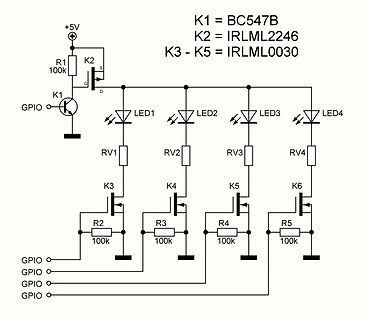
Schaltplan einer LED-Ansteuerung mit MOSFETs und GPIO
+5V, K1 = BC547B, K2 = IRLML2246, K3 - K5 = IRLML0030, R1 100k, K2, S, G, D, LED1 bis LED4, RV1 bis RV4, K3 bis K6, R2 bis R5 100k, GPIO
in „LED Matrix am Arduino über MOSFETs steuern“ · Analoge Elektronik und Schaltungstechnik · · Schaltpläne
-
 Bild
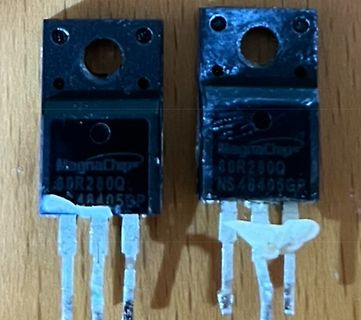
Zwei MagnaChip Leistungstransistoren auf Holzuntergrund
MagnaChip 80R280Q 48405GP
in „LG OLED65C97LA lässt sich nicht mehr einschalten“ · Analoge Elektronik und Schaltungstechnik · · Fotos
-
 Bild
Schaltplan mit 18650 Akku und MOSFET
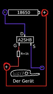
18650 + - A2SHB G S R=1k + - Der Gerät
in „18650 an Handy anschließen, Verpolschutz N Kanal Mosfet“ · Analoge Elektronik und Schaltungstechnik · · Schaltpläne
-
PDF
mosfet_Q1_Q4_sperren_nicht.pdf
mosfet_Q1_Q4_sperren_nicht.pdf
in „Mosfet BS208 sperrt nicht bei >3V“ · Analoge Elektronik und Schaltungstechnik ·
-
PDF
Mosfet_PHT8N06_Nkanal.pdf
Philips Semiconductors Product specification TrenchMOS transistor PHT8N06LT Logic level FET GENERAL DESCRIPTION QUICK REFERENCE DATA N-channel enhancement mode logic SYMBOL PARAMETER MAX. UNIT level field-effect power transistor in a plastic envelope suitable for surface V DS Drain-source voltage 55 V mounting. The device features very ID Drain current 7.5 A low on-state resistance and has P tot Total power dissipation 1.8 W integral zener diodes giving ESD T j Junction temperature 150 ˚C protection. It is intended for use in R Drain-source on-state 80 m DC-DC converters and general DS(ON) resistance
in „FET Konfektionierung okay?“ · Mikrocontroller und Digitale Elektronik ·
-
PDF
ecx10n16_Mosfet_Audio.pdf
Version 1.1 Exicon © is copyrighted and is a mark of Profusion plc. The information provided herein is believed to be reliable: however Profusion assumes no responsibility for inaccuracies or omissions. Profusion assumes no responsibility for the use of this information, and all use of such information shall be entirely at the users own risk. Specifications are subject to change without notice.
in „MOSFET für Audioverstärker?“ · Analoge Elektronik und Schaltungstechnik ·
-
PDF
KSQ_OPV_MOSFET_Auto_OFF_Schematics.pdf
+ V V+ LED+ 8 0 3 0 7 k R 2 R 2 5 8 IC1B R 4 7 6 LED- LM358N T1 k 4 1n 4 0 BUZ11 5 0 R 1 R 2 C1 R1 PK 510k 10k 0 K L D 1 R11 1 R10 3 IC1A 0 1 D1 9 0 2 4 6 4 10k 2 1N4148 2 R R 1 I L R 1 LM358N R 0 V- GND
in „Spannung für LED von 36V auf 34V senken“ · Analoge Elektronik und Schaltungstechnik ·
-
PDF
KSQ_OPV_MOSFET_Auto_OFF_Layout.pdf
V+ LED+ LED- R7 8 3 5 D1 R R R IC1 R R C1 T1 R1 1 R2 R R R KK1 V- IC2
in „Spannung für LED von 36V auf 34V senken“ · Analoge Elektronik und Schaltungstechnik ·
-
PDF
H-Bruecke-Mosfet-fuer_Seppermotor..sch.pdf
+48V +48V FQB4P06 FQB4P06 200K 200K M IRFZ48VSPbF IRFZ48VSPbF 1M 1M Das Gleiche nochmal
in „2 H-Brücken als Endstufe für Steppermotor“ · Analoge Elektronik und Schaltungstechnik ·
-
PDF
SMPD_MOSFET_and_IGBTs_Product_Brief.pdf
devices. IXYS is virtually the firstpowersemiconductorcompanytooffersurface-mountablehigh-voltagePowerMOSFETs and IGBTs. SMPD-B A ceramic isolation of up to 4.5kV is achieved with the Direct Copper Bond (DCB) substrate technology – an electrically isolated tab is provided for heat sinking. The DCB provides
in „IXYS Bauteil / Keine Info gefunden“ · Analoge Elektronik und Schaltungstechnik ·
-
 Bild
SMD-Bauteil auf Lineal
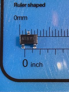
Ruler shaped 0mm 418Y1 0 inch
in „H-Brücke mit defektem MOSFET - Bauteil und Ursache bestimmen“ · Analoge Elektronik und Schaltungstechnik · · Fotos
-
PDF
MPQ4420H.pdf
Operating Input synchronous, rectified, step-down, switch-mode Range converter with built-in power MOSFETs. It • 90mΩ/55mΩ Low R DS(ON)Internal Power offers a very compact solution to achieve a 2A MOSFETs continuous output current with excellent load and line regulation over a wide input supply • High-Efficiency
in „DC-DC buck converter: Bauteile Identifikation“ · Analoge Elektronik und Schaltungstechnik ·
-
PDF
an-978_Bootstrap.pdf
low-side applications How to boost the output current of an MGD to drive Driving a high-side P-Channel MOSFET modules How to drive thyristor gates How to provide a continuous gate drive Troubleshooting guidelines 1.GATEDRIVEREQUIREMENTSOFHIGH-SIDEDEVICES The gate drive requirements for a power MOSFET or IGBT
in „IR2184 half bridgde driver / Ist PWM-Signal begrenzt?“ · Mikrocontroller und Digitale Elektronik ·
-
PDF
datasheet.pdf
current limit circuit uses the power supply is designed properly, current spikes caused by output MOSFET ON-resistance as a sense resistor. A current primary-side capacitances and secondary-side rectifier reverse limit comparator compares the output MOSFET on-state drain recovery time should not cause
in „Verzweifelt: Wie Widerstände und Kapazitäten eines Sperrwandler IC´s auslegen?“ · Analoge Elektronik und Schaltungstechnik ·
-
PDF
igbt_app-note.pdf
using - the Power MOSFET STP5N50 has an both types of power switch. The results are RDS(on)= 1.5 at 25°C and the IGBT given in Table 1. STGP10N50A has V CE(on)= 1.8V at I = 10A and T = 100°C. c Evaluation of the losses showed
in „AN- oder ABschnittsdimmer?“ · Mikrocontroller und Digitale Elektronik ·
-
PDF
igbt_app-note__alt_.pdf
using - the Power MOSFET STP5N50 has an both types of power switch. The results are RDS(on)= 1.5 at 25°C and the IGBT given in Table 1. STGP10N50A has V CE(on)= 1.8V at I = 10A and T = 100°C. c Evaluation of the losses showed
in „Dimmer mit Atmel Mega“ · Mikrocontroller und Digitale Elektronik ·
-
PDF
igbt_app-note__alt_.pdf
using - the Power MOSFET STP5N50 has an both types of power switch. The results are RDS(on)= 1.5 at 25°C and the IGBT given in Table 1. STGP10N50A has V CE(on)= 1.8V at I = 10A and T = 100°C. c Evaluation of the losses showed
in „Phasenan- bzw. abschnitt“ · Mikrocontroller und Digitale Elektronik ·
-
PDF
igbt_app-note__alt_.pdf
using - the Power MOSFET STP5N50 has an both types of power switch. The results are RDS(on)= 1.5 at 25°C and the IGBT given in Table 1. STGP10N50A has V CE(on)= 1.8V at I = 10A and T = 100°C. c Evaluation of the losses showed
in „PWM an Triac?“ · Mikrocontroller und Digitale Elektronik ·
-
PDF
igbt_app-note.pdf
using - the Power MOSFET STP5N50 has an both types of power switch. The results are RDS(on)= 1.5 at 25°C and the IGBT given in Table 1. STGP10N50A has V CE(on)= 1.8V at I = 10A and T = 100°C. c Evaluation of the losses showed
in „Triac entstören“ · Mikrocontroller und Digitale Elektronik ·
-
PDF
MRF150.pdf
MOTOROLA Order this document SEMICONDUCTOR TECHNICAL DATA by MRF150/D The RF MOSFET Line RF Power Field-Effect Transistor N–Channel Enhancement–Mode MRF150 Designed primarily for linear large–signal output stages up to150 MHz frequency range. Specified 50 Volts, 30 MHz Characteristics
in „Wärmeleitpad gesucht für POWER FET MRF150“ · Analoge Elektronik und Schaltungstechnik ·
-
PDF
hexiangning-20.pdf
PSpice models for power semiconductor devices such as diodes, bipolar junction transistors (bjt), and mosfets, which are based on their physical switching devices, which include the gate turn-off thyristor, the insulated gate bipolar transistor and the structure anduse the equivalent circuit method. But mos-controlled
in „Projekt: Leistungsstarkes Blitzgerät aus 12 Volt“ · Analoge Elektronik und Schaltungstechnik ·
-
PDF
schematics.pdf
06.02.2016 Sheetof File: C:\Users\..\can.SchDoc Drawn By: 1 2 3 4 1 2 3 4 A A V_SUPPLY P339kI3 U_mcu U_mosfet_driver U_mosfets R4 mcu.SchDoc mosfet_driver.SchDoc mosfets.SchDoc P42k2I4 LS CD0603 D6 C2 EN_GATE EN_GATE M_H1 M_H1 PHASE_1 VccPIX101 PD0 PD0 5V GND PC0P100nF AN_IN H1 H1 M_L1 M_L1 PIX102SB_N PR022R1003
in „BLDC Motorcontroller 200A 48V basierend auf VESC“ · Analoge Elektronik und Schaltungstechnik ·
-
PDF
MAX1700-MAX1701.pdf
During the the level to which the inductor current is allowed to second part of each cycle, when the MOSFET is turned ramp during each cycle and modulates the MOSFET off, the voltage across the inductor reverses and forces switch pulse width. A second comparator enforces an current through the diode and
in „5V Spannung aus Lipo?“ · Mikrocontroller und Digitale Elektronik ·
-
PDF
Viper12A.pdf
WIDE RANGE V DD VOLTAGE DIP-8 VIPer12ADIP n CURRENT MODE CONTROL n AUXILIARY UNDERVOLTAGE LOCKOUT MOSFET on the same silicon chip. Typical WITH HYSTERESIS applications cover off line power supplies for battery charger adapters, standby power supplies n HIGH VOLTAGE START UP CURRENT for TV or monitors,
in „LiIon 18650 Ladegerät für zwei Parallel“ · Mikrocontroller und Digitale Elektronik ·