-
Thread
Messen von Dioden mit Multimeter
nur verstehen was du mit enorm falsch meinst. Aber richtig, bei kleinen DC DC Wandler für High Side Gate Treiber die bei 1W liegen und 5-6 unabhängige Wicklungen haben ist der Fehler deutlich größer wenn man K=1 setzen würde
verstehen was du mit enorm falsch meinst. > > Aber richtig, bei kleinen DC DC Wandler für High Side Gate Treiber die > bei 1W liegen und 5-6 unabhängige Wicklungen haben ist der Fehler > deutlich größer wenn man K=1 setzen würde Wir haben in der UNI 2 stück gemessen zum einen knickt der Übertrager
-
 Bild
Bild
Tabelle mit Absolutmaxima und Blockschaltbild eines Gate-Treibers
2 Absolute maximum ratings Parameter Symbol Values Unit Note / Test Condition Power supply output side VCC2 Min. -0.3 Max. 40 V 1) Gate driver output VOUT GND2-0.3 VCC2+0.3 1) Positive power supply input side VCC1 Min. -0.3 Max. 18.0 V - Logic input voltages (IN+, IN-) VLogicIN Min. -0.3 Max. 18.0 V

-
 Bild
Bild
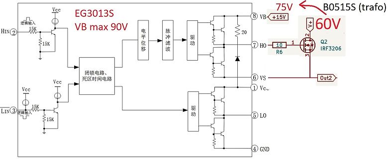
Schaltplan eines Gate-Treiber-ICs mit MOSFET-Ausgang
EG3013S VB max 90V HIN 15K 15K Vcc 电平移 脉冲滤波 驱动 死区时间电路 闭锁电路 8 VB +15V 75V B0515S (trafo) 60V V+ 10 R6 2 IRF3206 Q2 6 VS Out2 1 Vc 5 LO 4 GND
-
Thread
Platinendesign
de.rs-online.com/web/c/?pn=1&searchTerm=lochrasterplatine&rpp=20&selectedNavigation=attributes.Number_of_Sides=2
-
 Bild
Bild
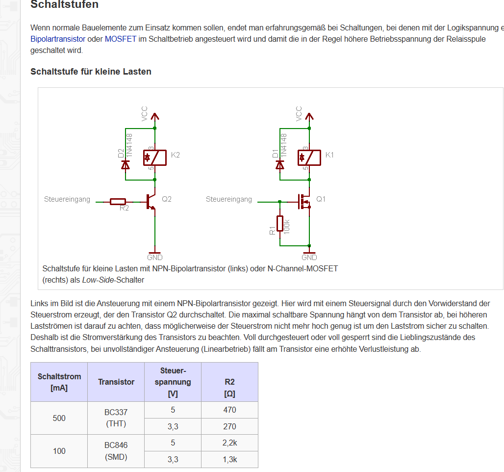
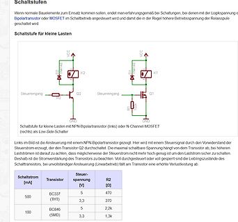
Schaltplan und Tabelle für Transistor-Schaltstufen
Schaltstufe für kleine Lasten mit NPN-Bipolartransistor (links) oder N-Channel-MOSFET (rechts) als Low-Side-Schalter VCC, D2, 1N4148, K2, Steuereingang, Q2, R2, GND, D1, 1N4148, K1, Steuereingang, Q1, R1, 100k, GND Schaltstrom [mA], Transistor, Steuerspannung [V], R2 [Ω] 500, BC337 (THT), 5, 470 , 3,3, 270
-
Thread
Wertige 4mm Buchsen gesucht
index.html?ACTION=446&SEARCH=laborbuchse&START=0&OFFSET=100&LA=0&nbc=1&q=laborbuchse&q=laborbuchse&SID=925269006a5e50254d025c7dc663fa2c308820023b3a41e7453bc
-
Thread
Absicherung von Digitalen Ausgängen
Schutz vor "versehentlich 230V angeschlossen" gefragt. Infineon Profet (Automotive Smart High-Side Switch) schalten Lasten und schützen sich selbst einigermaßen. Für Logiksignale unter 1 MHz reicht meist ein R/C Filter (100 Ohm, 1 nF) am Ausgang und Eingang, um gegen Berührung und Radiowellen
Ja, neee.... https://www.infineon.com/cms/de/product/power/smart-power-switches/high-side-switches/profet-industrial-smart-high-side-switch/its4100s-sj-n/
-
 Bild
Bild
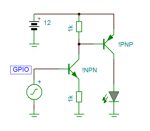
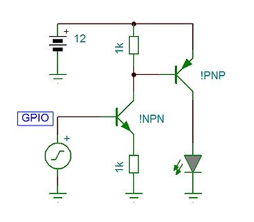
Schaltplan mit NPN- und PNP-Transistor zur LED-Ansteuerung
12, 1k, !PNP, !NPN, GPIO, 1k
-
Thread
Mit BC807 12v-LED schalten
LED-Modul. Ist es auch, wenn du dir nicht unbedingt in den Kopf setzt, auf der 12V-Seite (high-side) zu schalten. Warum?
schon oft genug behandelt. Aber weshalb High Side? Um es unnötig kompliziert und aufwendig zu machen?
-
Thread
Wie 20-40A high side (n-Ch 2,4 mOhm) bei 20-60V und 2 kHz 50% duty pwm ?
Wie 20-40A high side (n-Ch 2,4 mOhm) bei 20-60V und 2 kHz 50% duty pwm ?
wirklich 100V und viel mehr zu schaffen, Weil sie halt low-side und high-side bedienen.. Trotzdem für mich Verschwendung, die low-side einfach links liegen zu lassen..
-
 Bild
Bild
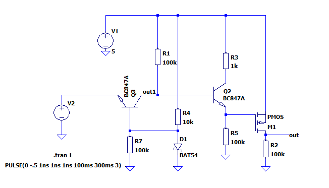
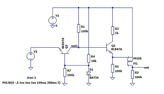
Schaltplan einer Transistorschaltung
V1 5 R1 100k Q3 BC477A out1 R4 10k V2 Q2 BC847A R3 1k D1 BAT54 R7 100k R5 100k M1 PMOS R2 100k out .tran 1 PULSE(0 -0.5 1ns 1ns 100ms 300ms 3)
-
Thread
High Side Switch Mosfet
Hallo, ich möchte zwei verschiedene High-Side Power Switch für mein Messboard aufbauen. Schaltung 1.) Ganz normaler High Side welcher mit +3,3V den Mosfet durchschaltet, um meine 5V durchzuschalten. Die nachfolgende Schaltung benötigt lediglich
-
 Bild
Bild
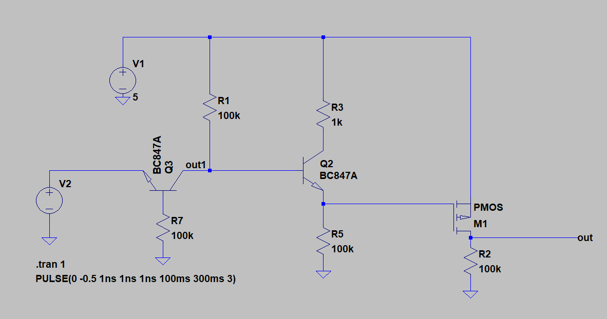
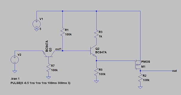
Schaltplan einer Transistorschaltung mit PMOS
V1 5 R1 100k R3 1k Q2 BC847A R5 100k M1 PMOS out R2 100k Q3 BC847A out1 V2 R7 100k .tran 1 PULSE(0 -0.5 1ns 1ns 100ms 300ms)
-
 Bild
Bild
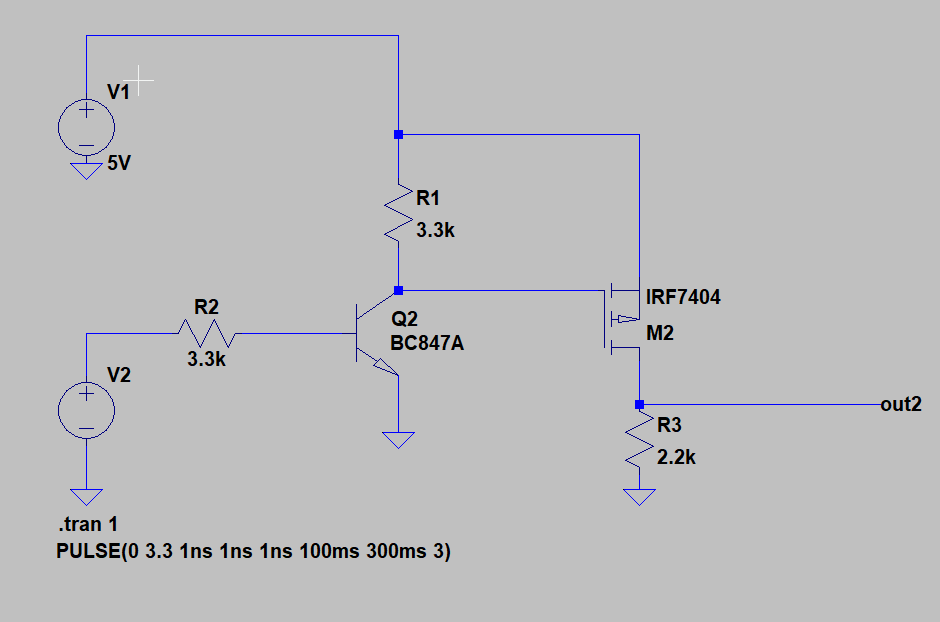
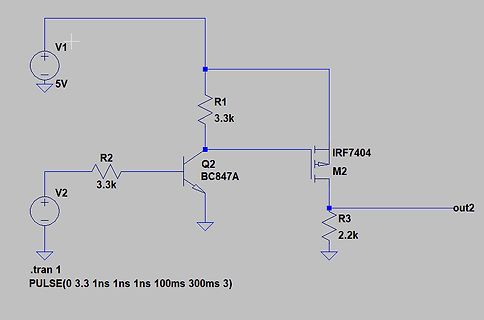
Schaltplan mit Transistor und MOSFET
V1 5V R1 3.3k Q2 BC847A R2 3.3k V2 IRF7404 M2 R3 2.2k out2 .tran 1 PULSE(0 3.3 1ns 1ns 100ms 300ms 3)
-
Thread
gutaussehnde Gehäuse
Du darin verpackt hast; https://upload.wikimedia.org/wikipedia/commons/5/54/Imac_G3_5_flavors_side_lineup.jpg
-
Thread
DC DC Spannungswandler 24 auf 12 40A stribt
sein könnte. Das Ansteuern des N-Kanal-Mosfet im unteren Zweig ist nun mal viel einfacher als High-Side.
Und der Strom wird gemessen über die Spannung an R14 am Drain der Low-Side-MOSFETs. Der Schaltplan sieht ziemlich schlampig aus. Die Z-Diode U5 mit drei Anschlüssen verstehe ich überhaupt nicht.
-
 Bild
Bild
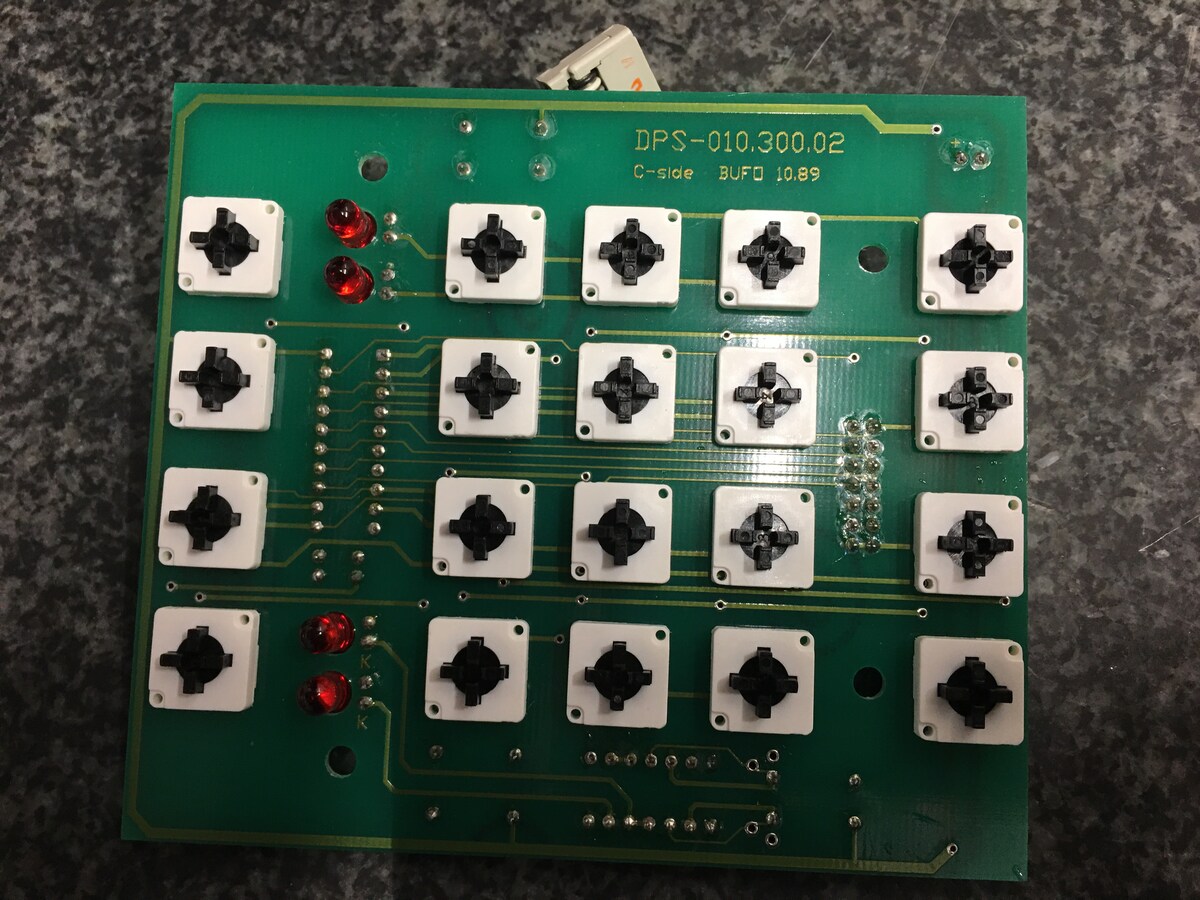
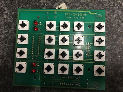
Grüne Leiterplatte mit mechanischen Schaltern und LEDs
DPS-010.300.02 C-side BUFD 10.89
-
 Bild
Bild
Infineon PSOC Edge Produktinformationsblatt
12S), 10/100 Ethernet, 2x CAN FD, 2x Smart IO, USB HS/FS or PIF Secure Enclave Secure Key Storage, Side Channel Attack Resistance, Crypto Accel., Secure Boot, Tamper Protect System Resources Power Management, Clock Control, TRNG, OTP, Secure JTAC, LVD, WCD, ECO, RTC, Active LDOs, 3x LPTIM, Buck Converters

-
Thread
SAT-Receiver startet immer langsamer
Always look on the bright side of life!
-
Thread
billige sehr gut erhältliche Instrumentenverstärker gesucht
=446&SEARCH=instrumentenverst%C3%A4rker&START=0&OFFSET=16&LA=0&nbc=1&q=instrumentenverst%C3%A4rker&SID=931ff70c393299434a463aebd0d6b7f33403e6d8a54cb2b9ae386 mfg klaus
-
 Bild
Bild
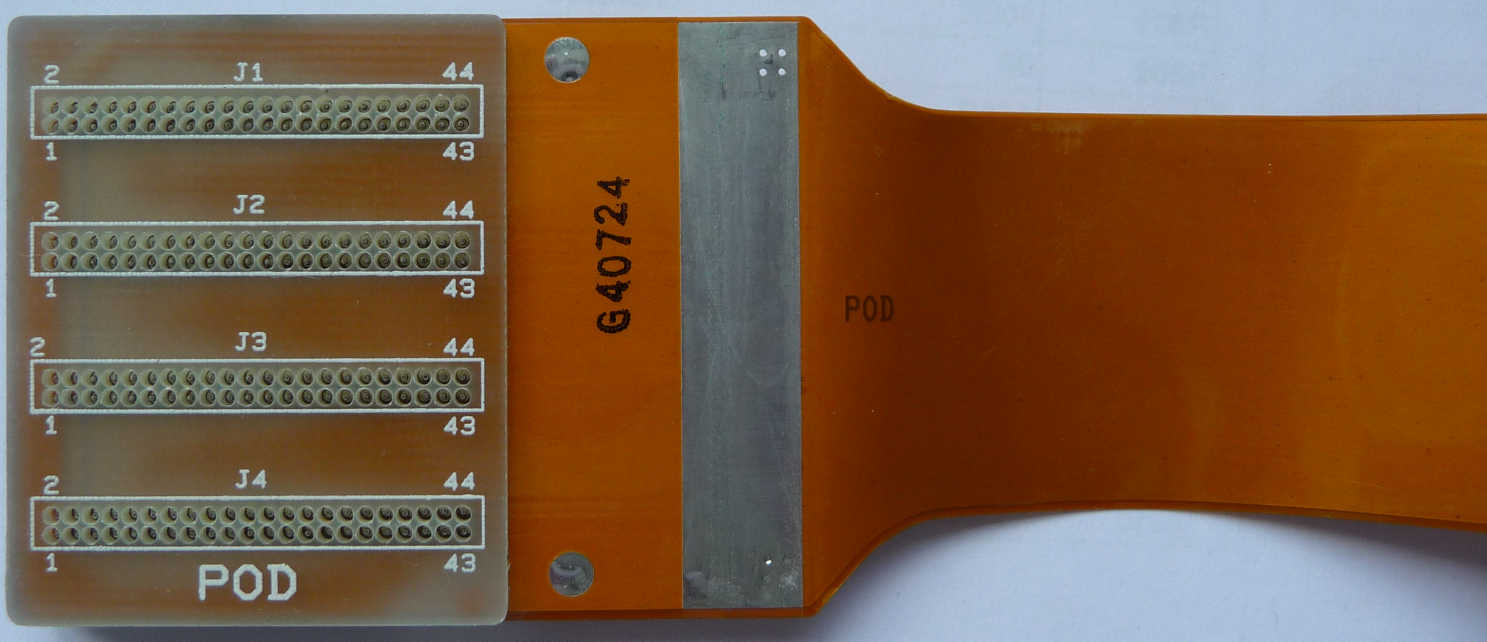
Flexibles Flachbandkabel mit Anschlussleisten
J1 2 44 1 43 J2 2 44 1 43 J3 2 44 1 43 J4 2 44 1 43 G40724 POD POD

-
Thread
Eagle 9.6.2 Installation unter Linux bringt Fehler
Danke Harald, ich denke ich hab das richtige Package jetzt gefunden: https://packages.debian.org/sid/libgl1-mesa-dri Viele Grüße, Georg
#7643742: > ich denke ich hab das richtige Package jetzt gefunden: > https://packages.debian.org/sid/libgl1-mesa-dri Eigentlich wäre es der Job eines Installers, fehlende Abhängigkeiten zu finden und mit zu installieren...
-
 Bild
Bild
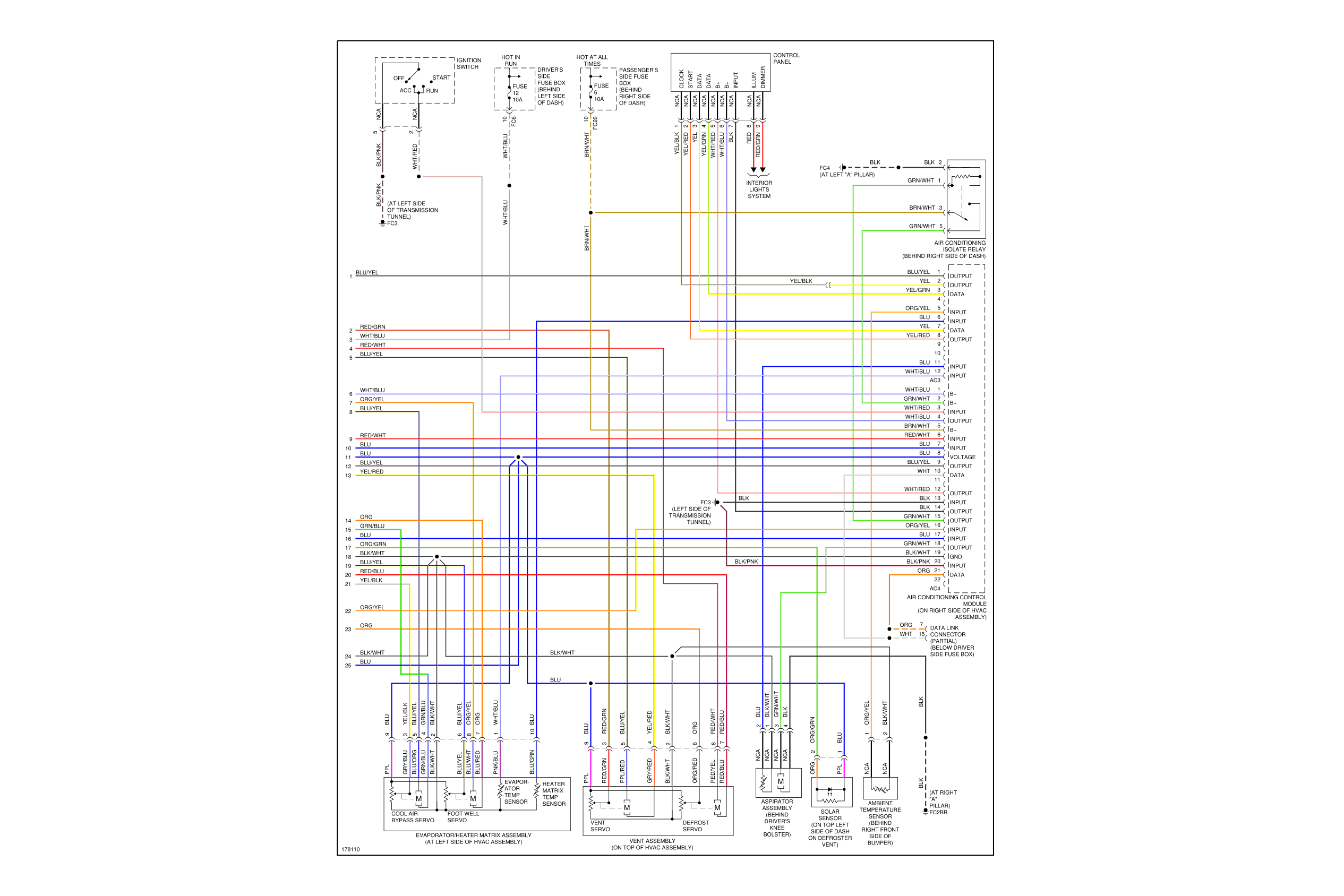
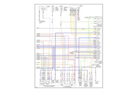
Verdrahtungsplan eines Fahrzeugsystems
IDENTIFICATION NUMBER, HOT IN, START, FUSE BOX, DRIVER SIDE FUSE, PASSENGERS SIDE FUSE, CONTROL PANEL, LEFT SIDE TRANSMISSION CHANNEL, AIR CONDITIONING, RIGHT SIDE, DATA LINK, FUSE BOX, EVAPORATOR, HEATER MATRIX ASSEMBLY, VENT ASSEMBLY, DETROIT SIDE OF BOLSTER, AIR CONDITIONING, DATA LINK, PASSENGERS SIDE OF HANDLE, RIGHT SIDE OF HANDLE
-
Thread
# Was ist das für ein Relais HFD2/005-M-D(555) ?
Auf dem Relais steht "HFD2/005-M-D(555)" laut Bild vom Verkäufer. Also 5V Version als "Single Side Stable" = also normales Relais, Strom an= umschalten, Strom aus = wieder zurück ? Aber was dann nach dem "-M" kommt finde ich nicht im Datenblatt, denn irgendwie übersehe ich was oder verstehe es
Nil bedeutet, dass die Angabe fehlt. Du hast da die Single Side Stable Version. Das 'D' ist dann schon das Kontaktmaterial. Single Side Stable ist ein normales Relais.
-
Thread
Ersatz für Ringkabelschuh
index.html?ACTION=446&SEARCH=temperatursicherung&START=0&OFFSET=30&LA=446&nbc=1&q=temperatursicherung&SID=9287a89daf4f151446ae48f4aab07db41bcb19c007d7d258c6846 > (Blöde Suchfunktion, ich hatte auf 184° beschränkt, aber das steht nicht > in der langen URL.) > Auch Conrad nennt sie "Temperatursicherung
index.html?ACTION=446&SEARCH=temperatursicherung&START=0&OFFSET=30&LA=446&nbc=1&q=temperatursicherung&SID=9287a89daf4f151446ae48f4aab07db41bcb19c007d7d258c6846 > (Blöde Suchfunktion, ich hatte auf 184° beschränkt, aber das steht nicht > in der langen URL.) Reichelt kann nichts für Internetlegastheniker
-
Thread
STM32 Bootloader Write Command ACK aber kein Write
AN3155 "USART protocol used in the STM32 bootloader", Figure 13. "Write Memory command: device side". Steht da irgendetwas von "erase"??? Wie soll der ärmste auch wissen, ob man nur ein Byte neu schreiben will und der Rest des Sektors so ungefragt übern Jordan gehen soll/darf? Die Verantwortung
-
Thread
ESP32-C6-XIAO, neue Cortex-M23-Mikrocontroller, OpenBSD 7.5 und mehr
per-CPU caching for the VP pool and PTE descriptor (PTED) pool in the PMAP implementation to reduce side effects of locking contention on the kernel map lock. In turn this leads to "significant speedups" for many-core ARM64 systems like AArch64 servers. . . . - New driver support for the Allwinner D1
-
Thread
IR2136 Motorendstufe spinnt
#7642626: > Hatte mir da mal etwas rausgezeichnet... Da ist ja ein Shunt zu sehen. Sogar low-side. Da dran könntest du mal versuchen, auf einem weiteren Kanal des Oszi den Strom zu messen. LG, Sebastian
-
Thread
Tasmota SML / DWS7420 - ungültige Daten
1,77070100020800ff@1000,Lieferung,kWh,en_out,4 1,77070100100700ff@1,Leistung,W,power,2 1,7707010060320101@#,SID,,meter_id,0 # Als Ausgabe im Debugmodus erhalte ich: 17:25:31.983 : 77 07 01 00 01 08 00 ff 60 1c 81 04 72 62 01 62 00 62 1e 52 ff 60 0e 45 d8 01 17:25:32.030 : 77 07 01 00 02 08 00 ff 00
-
Thread
Probleme mit Spannungsunterschieden beim Schalten
DENSELBEN PRINZIP der Schaltung mit 15 und 100 Volt > machen. Ganz sicher nicht. Das geht "Low Side" ganz problemlos. Bei dir ist aber einer der N-Kanal-Mosfets "High Side". Da braucht man ein "ANDERES PRINZIP" zum Ansteuern. Wenn man den Schaltplan vernünftig zeichnet, sieht man auch was Low- und High-side ist, einfach weil die FETs dann auch oben und unten im Schaltplan liegen.
-
Thread
init.lua nvim probleme
col = 0, -- the column to display the pet at (set to high number to have it stay still on the right side) speed_multiplier = 1, -- you can make your pet move faster/slower. If slower the animation will have lower fps. default_pet = "dog", -- the pet to use for the PetNew command default_style
-
Thread
Altium Designer - Assistent zur manuellen Bauteilbestückung
Panel PCB, kann man oben anstelle von Nets Components auswählen und dann die Components Class "Top Side Components" (oder Bottom, je nachdem). Dann bekommt man eine Liste aller Bauteile, welche man bspw. nach Wert sortieren kann und dann einfach durchgehen kann. So kommt man relativ schnell von Bauteil