Telephone and data communication electromotiveforceprotectiondiodein the drive circuits on the input side equipment TYPES Part No. Output rating* Through hole Packing quantity terminal Surface-mount terminal Type Tape and reel packing style Load Load Tube packing style Picked from the Picked from the Tube Tape and reel voltage current 1/2/3-pin side 4/5/6-pin side 1 tube contains 50 pcs. AC/DC type 400 V 120 mA AQV234 AQV234A AQV234AX AQV234AZ 1 batch contains 1,000 pcs. 500 pcs. *Indicate the peak AC and DC values. Note: For space reasons, the
electromotiveforceprotectiondiodein 2.Telephone and data communication the drive circuits on the input side equipment TYPES Part No. Output rating* Through hole Packing quantity terminal Surface-mount terminal Type Load Load Tape and reel packing style voltage current Tube packing style Picked from the Picked from the Tube Tape and reel 1/2/3-pin side 4/5/6-pin side 1 tube contains 50 pcs. AC/DC type 400 V 120 mA AQV234 AQV234A AQV234AX AQV234AZ 1,000 pcs. 1 batch contains 500 pcs. *Indicate the peak AC and DC values. Note: For space reasons, the
and minimum bending radius; tape type II, embossed carrier tape with top cover tape on the upper side; max. pieces of filters per reel: 3000 reel of empty components at start: min 300 mm reel of empty components at start including leader: min 500 mm trailer min 300 mm Tape (all dimensions in mm) EMBOSSED
below. The two photodiodes are closely matched, with PD1 on the input Bandwidth(LED) 9MHztyp 9MHztyp side and the PD2 on the output side of the application circuitry. The output current of the photodiode is linearly related to the light CommonModeNoise 95dB typ 95dB typ output of the LED. Having an input
Produce Soldering applications for high flexibility and high throughput independently of each other side by side. Board sizes up to 685 mm. CAD expert mode. High Five for Ultimate Selective Soldering.
from the edge of the board toward the rear. Bind them so that the bound part will come to the upper side of Side A. SLMB Assy Binder SLOTIN MECHA Assy Bottom view 3 B Bound part Side A OK Rear side Cable Side B Side A Side B NG Side A NG Side B C D E F CDJ-350 41 5 6 7 8 Downloaded from www.Manualslib.com
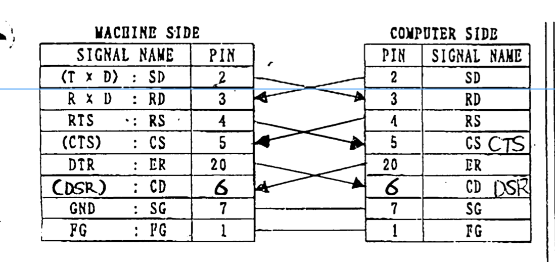
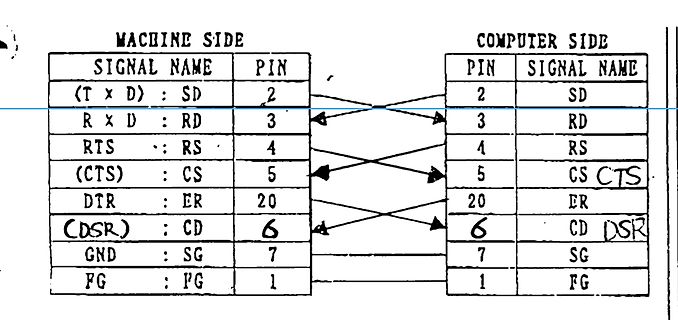
MACHINE SIDE
SIGNAL NAME PIN
(T x D) : SD 2
R x D : RD 3
RTS : RS 4
(CTS) : CS 5
DTR : ER 20
(DSR) : CD 6
GND : SG 7
FG : FG 1
COMPUTER SIDE
PIN SIGNAL NAME
2 SD
3 RD
4 RS
5 CS CTS
20 ER
6 CD DSR
7 SG
1 FG
voltage Load current Tube packing style Picked from the Picked from the Tube Tape and reel 1/2/3-pin side 4/5/6-pin side 40 V 500 mA AQV251 AQV251A AQV251AX AQV251AZ 60 V 400 mA AQV252 AQV252A AQV252AX AQV252AZ 100 V 350 mA AQV255 AQV255A AQV255AX AQV255AZ 1 tube contains 200 V 250 mA AQV257 AQV257A AQV257AX
voltage Load current Tube packing style Picked from the Picked from the Tube Tape and reel 1/2/3-pin side 4/5/6-pin side 40 V 500 mA AQV251 AQV251A AQV251AX AQV251AZ 60 V 400 mA AQV252 AQV252A AQV252AX AQV252AZ 100 V 350 mA AQV255 AQV255A AQV255AX AQV255AZ 1 tube contains 200 V 250 mA AQV257 AQV257A AQV257AX
ZXCT1041 Bidirectional precision high-side current monitor Description The ZXCT1041 is a bidirectional precision high- The very low offset voltage enables a typical side current sense monitor. The output voltage accuracy of 2% for sense voltages
mum value for R .1Thus, to ground, which can over- FMMT597 for supply rails of 100 to load the high-side drive cir- OUTPUT R 250V,a reasonable R 1 val- cuitry. To avoid such poten- (10 mV/mA) 150k ue is 150 to 225 k⍀—150 tial fault conditions, you 17.5V FULL-SCALE 10k k⍀ in this case. should use a high-side
voltage Load current Tube packing style Picked from the Picked from the Tube Tape and reel 1/2/3-pin side 4/5/6-pin side 40 V 500 mA AQV251 AQV251A AQV251AX AQV251AZ 60 V 400 mA AQV252 AQV252A AQV252AX AQV252AZ 100 V 350 mA AQV255 AQV255A AQV255AX AQV255AZ 1 tube contains 200 V 250 mA AQV257 AQV257A AQV257AX
L = 80 cm - 33 50 mA 1, 2 NOTES: 1. Measurements made with Kodak R-27 Gray Card, using the white side, (90% reflectivity). 2. L = Distance to reflective object. VCC (POWER SUPPLY) 38.3 ms ±9.6 ms DISTANCE MEASURMENT OPERATING 1st 2nd nth MEASUREMENT MEASUREMENT MEASUREMENT V (OUTPUT) UNSTABLE 1st 2nd
Data Word Transfer Timing —4.5 V VSS —0 V PRZ POR RESW t t RESS BUSY SCLK Data Word Data Word MSB side LSB side MSB side LSB side 9/16 ¡ Semiconductor MSC1937-01 FUNCTIONAL DESCRIPTION TheMSBvalueof8-bitserialdatadetermineswhethertheinputdataintoMSC1937-01iscontrol data or display data. Display Data
voltage Load current Tube packing style Picked from the Picked from the Tube Tape and reel 1/2/3-pin side 4/5/6-pin side 40 V 500 mA AQV251 AQV251A AQV251AX AQV251AZ 60 V 400 mA AQV252 AQV252A AQV252AX AQV252AZ 100 V 350 mA AQV255 AQV255A AQV255AX AQV255AZ 1 tube contains 200 V 250 mA AQV257 AQV257A AQV257AX
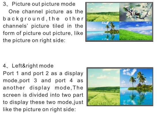
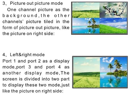
background,the other channels' picture tiled in the form of picture out picture, like the picture on right side:
4. Left&right mode
Port 1 and port 2 as a display mode,port 3 and port 4 as another display mode,The screen is divided into two part to display these two mode,just like the picture on right side:
fi PROFET ITS 716G Smart High-Side Power Switch For Industrial Applications Four Channels: 4 x 140mΩ Status Feedback Product Summary Package PG-DSO-20 Operating Voltage Vbb 5.5 ...40V Operating Temperature T -30 +85°C a Active channels
Names Description 1 X OE n Output Enable Input (Active LOW) C V T/Rn Transmit/Receive Input 4 A –A Side A Inputs or 3-STATE Outputs 7 0 15 B 0B 15 Side B Inputs or 3-STATE Outputs NC No Connect FBGA Pin Assignments 1 2 3 4 5 6 A B0 NC T/R1 OE 1 NC A 0 B B2 B1 NC NC A 1 A 2 C B4 B3 VCCB VCCA A 3 A 4 D
V11 DOC REV:V11.1 Date:2011-11-12 Page: 12 of 23 INANBO 26 Y- - Touch panel coordinate in the down side of envisage drawing. 27 X- - Touch panel coordinate in the left side of envisage drawing. 28 Y+ - Touch panel coordinate in the up side of envisage drawing. 29 X+ - Touch panel coordinate in the right side of envisage drawing. 30 LED-1 - LED light cathode. 31 LED-2 - LED light cathode. 32 LED-3 - LED light cathode. 33 LED-4 - LED light cathode. 34 LED-5 - LED light cathode. 35 LED-A - LED light anode.
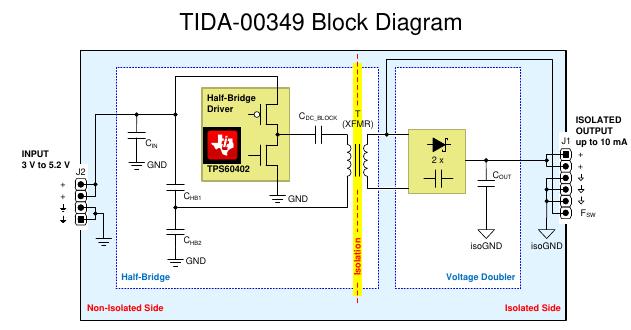
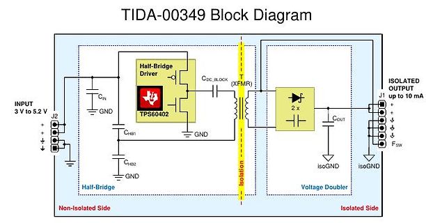
as close as possible to the related pin. 0 t Cp is the DC blocking cap in the transformer primary side. It conducts large winding current 3ms (typically 0.8ARMS), so low ESR X7R/X5R Figure 2—Input Voltage vs. Enable ceramic is required. The capacitance value is typically 0.47µF to 2.2µF. The voltage
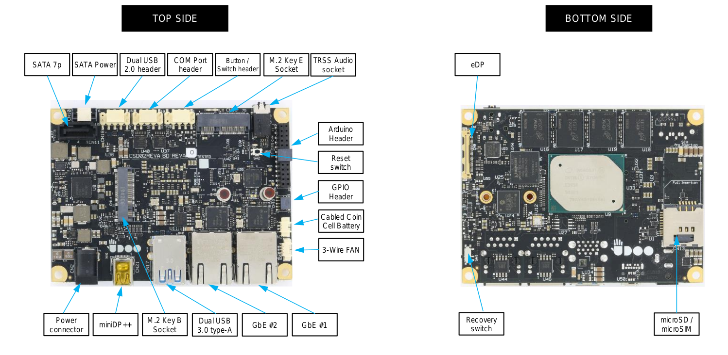
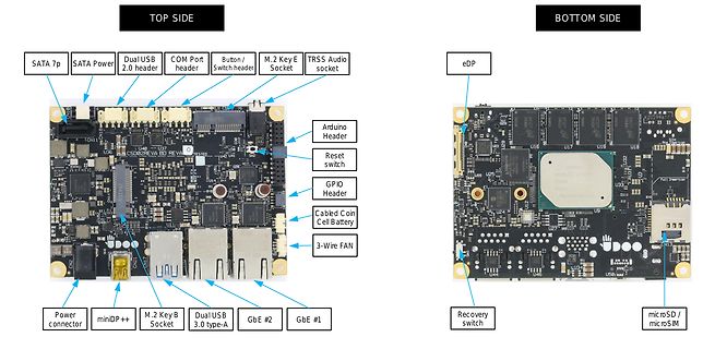
TOP SIDE BOTTOM SIDE SATA 7p SATA Power Dual USB 2.0 header COM Port header Button / Switch header M.2 Key E Socket TRSS Audio socket Arduino Header Reset switch GPIO Header Cabled Coin Cell Battery 3-Wire FAN
Minor 7 Plate discoloring No plate fading, rusting and discoloring Minor 8 Solder amount a. Soldering side of PCB Minor Solder to form a ‘Filet’ 1. Lead parts all around the lead. Solder should not hide the lead form perfectly. (too much) b. Components side ( In case of ‘Through Hole PCB’) Solder to reach the Components side of PCB. 2. Flat packages Either ‘Toe’(A) or ‘Seal’(B) of Minor the lead to be covered by ‘Filet’. A B Lead formto be assume over solder. 3. Chips (3/2) H ≥ h ≥ (1/2) H Minor h H 9 Solder ball/Solder
edited board. 12 Here is a snap shot of the above board in SprintLayout Photo view mode (both board sides): This is exactly what the board will look like when it is manufactured. Top Side Bottom Side 13 Some important notes on editing 274-X converted Gerbers in SprintLayout In general the converted file
Entry Modules (PEMs) UL and CSA listed The shelves provide lug attachments of output power on either side from the rear. Each lug can VDE licensed carry up to 100 Amperes for a total of 200 Amperes per shelf. CE mark meets 73/23/EEC and 93/68/EEC directives Input power can be delivered by C13 IEC-320, AMP
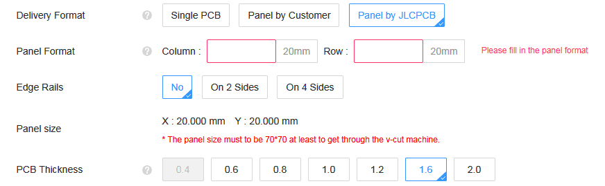
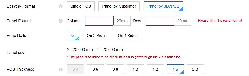
by JLCPCB Panel Format Column : 20mm Row : 20mm Please fill in the panel format Edge Rails No On 2 Sides On 4 Sides X : 20.000 mm Y : 20.000 mm * The panel size must be 70*70 at least to get through the v-cut machine. Panel size PCB Thickness 0.4 0.6 0.8 1.0 1.2 1.6 2.0
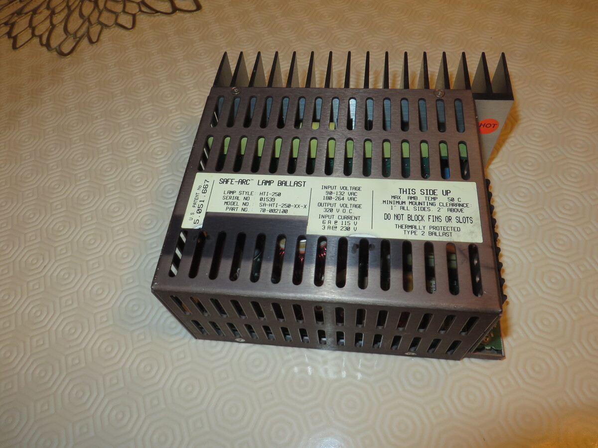
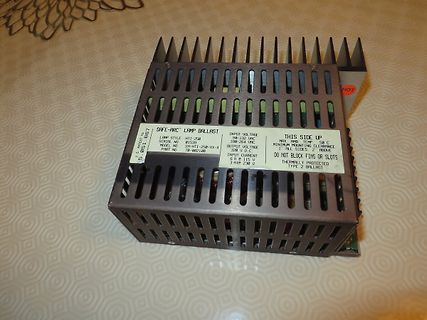
INPUT VOLTAGE 98-132 VAC
180-264 VAC
OUTPUT VOLTAGE 520 V
INPUT CURRENT 6 A @ 132 V
3 A @ 230 V
THIS SIDE UP
MAX TEMP 50 °C
MINIMUM MOUNTING CLEARANCE 1" ALL SIDES 2" ABOVE
DO NOT BLOCK FINS OR SLOTS
THERMALLY PROTECTED TYPE 2 BALLAST
PATENT NO 5 051 667
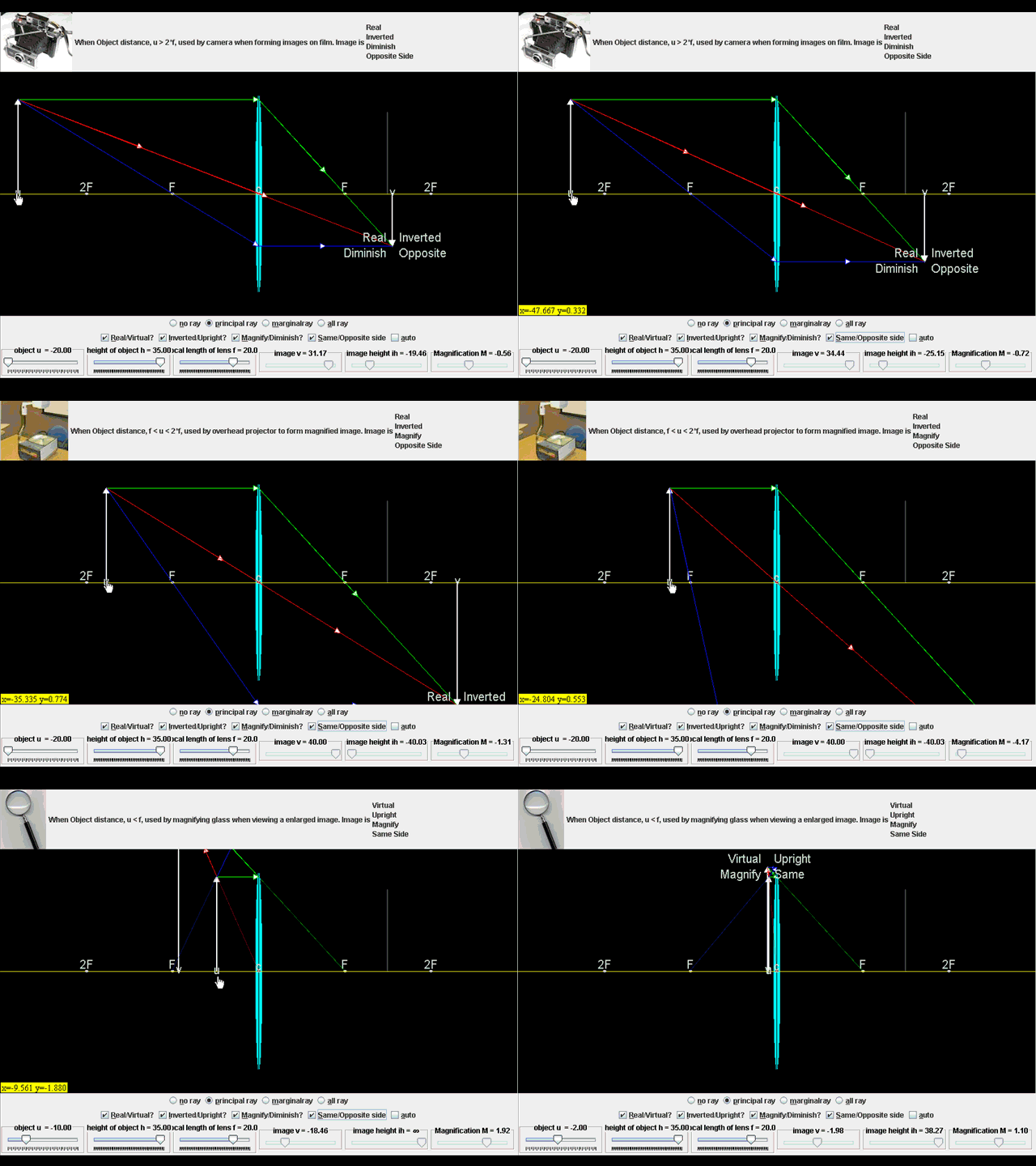
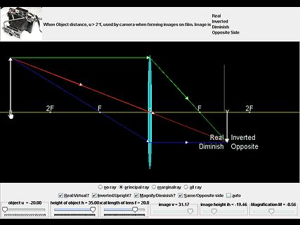
f, used by magnifying glass when viewing an enlarged image. Image is Virtual Upright Magnify Same Side 2F F F 2F Virtual Upright Magnify Same no ray principal ray marginalray all ray Real/Virtual? Inverted/Upright? Magnify/Diminish? Same/Opposite side auto object u = -2.00 height of object h = 35.00
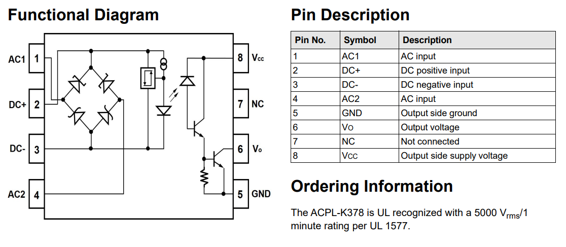
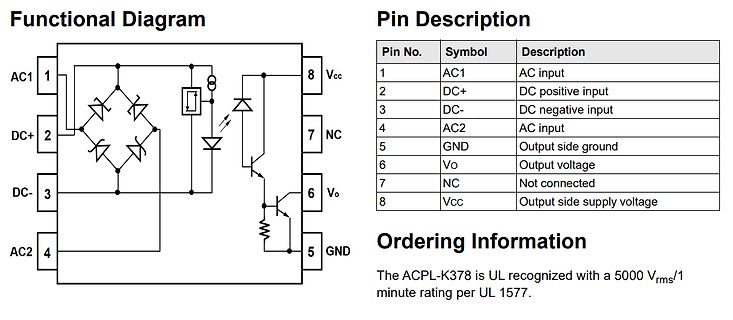
Description
1 AC1 AC input
2 DC+ DC positive input
3 DC- DC negative input
4 AC2 AC input
5 GND Output side ground
6 Vo Output voltage
7 NC Not connected
8 Vcc Output side supply voltage
Ordering Information
The ACPL-K378 is UL recognized with a 5000 Vrms/1 minute rating per UL 1577.
as seen by the slave when a P82B96 is substituted. P82B96 uses a static level offset on the slave side to isolate noise and loadings on either side of this device. The nominal offset is 0.8 V and that V OL may create worst-case design tolerance problems with slave devices that do not use I C-bus2 switching
Serial Clock 14 — SDA Serial Data 15 — DACV Voltage DAC Output 16 12 PGND Power Ground 17 13 DLO Low-Side Power MOSFET Driver Output 18 14 DHI High-Side Power MOSFET Driver Output 19 15 LX Power Connection for the High-Side Power MOSFET Driver 20 16 BST Power Connection for the High-Side Power MOSFET Driver
Serial Clock 14 — SDA Serial Data 15 — DACV Voltage DAC Output 16 12 PGND Power Ground 17 13 DLO Low-Side Power MOSFET Driver Output 18 14 DHI High-Side Power MOSFET Driver Output 19 15 LX Power Connection for the High-Side Power MOSFET Driver 20 16 BST Power Connection for the High-Side Power MOSFET Driver
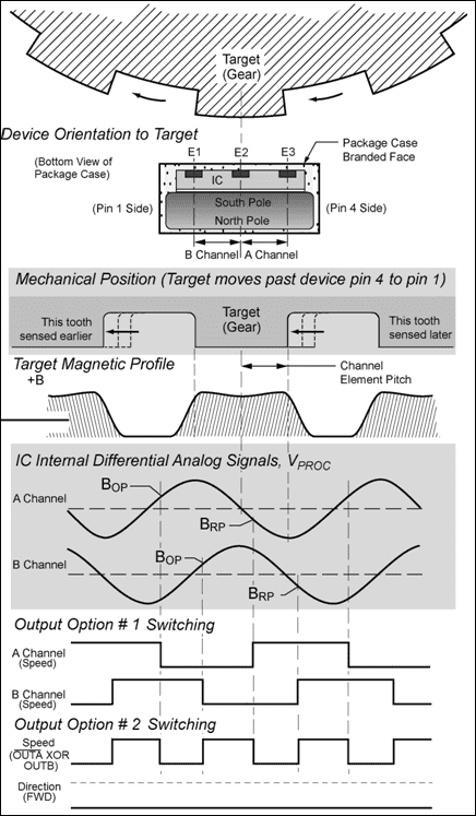
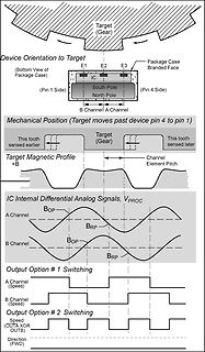
(Bottom View of Package Case)
E1 E2 E3
Package Case Branded Face
IC
South Pole
North Pole
(Pin 1 Side) (Pin 4 Side)
B Channel A Channel
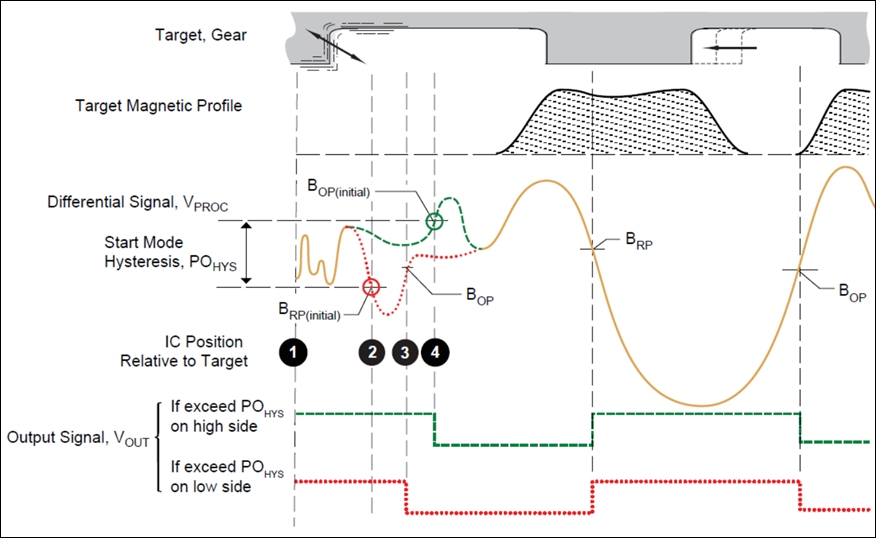
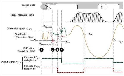
Mechanical Position (Target moves past device pin 4 to pin 1)
This tooth sensed earlier
Target (Gear)
This tooth sensed later
Target Magnetic Profile
+B
Channel Element
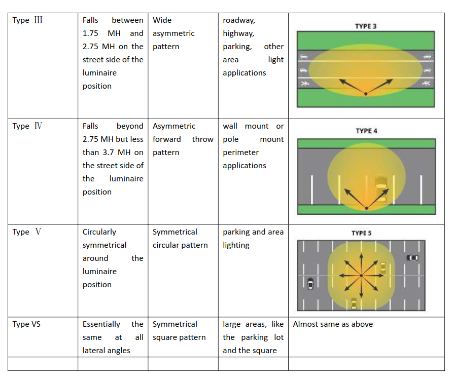
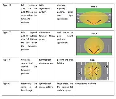
Type III Falls between 1.75 MH and 2.75 MH on the street side of the luminaire position Wide asymmetric pattern roadway, highway, parking, other area light applications TYPE 3 Type IV Falls beyond 2.75 MH but less than 3.7 MH on the street side of the luminaire
Voltage 1" ] pack [ ttk::entry .nb.classic.inputvoltage1.entry -width 15 -textvariable input_voltage1] -side right -fill x; } Neu: # hbs_global_com_open = Flag für COM Port geöffnet und verbunden if {hbs_global_com_open == 1} { # Setting up the Primary Voltage1 if COM Port is open grid [ttk::labelframe .nb.classic.inputvoltage1
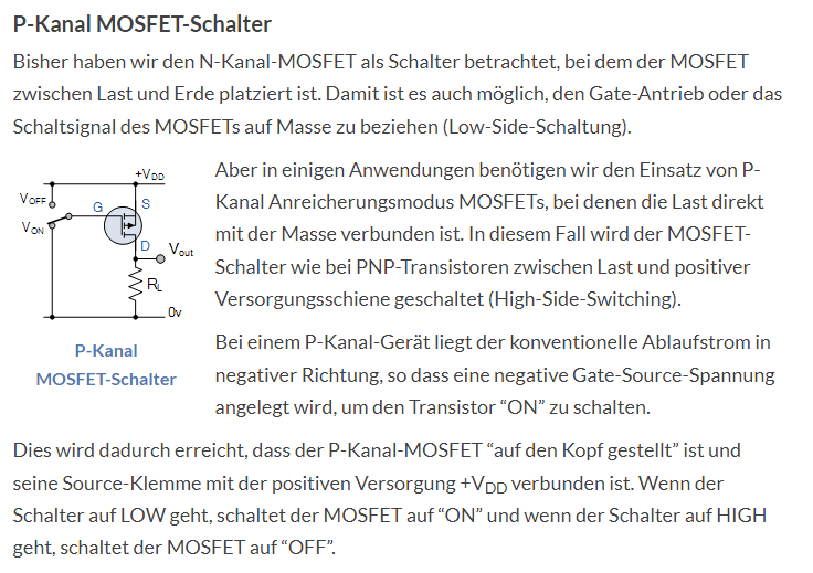
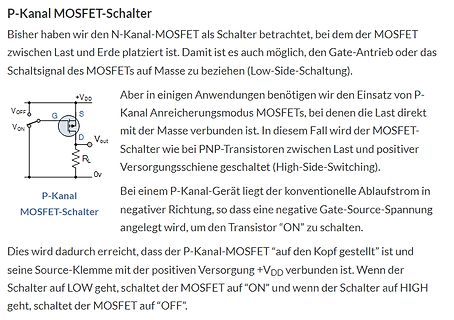
Damit es auch möglich, den Gate-Antrieb oder das Schaltsignal des MOSFETs auf Masse zu beziehen (Low-Side-Schaltung).
Aber in einigen Anwendungen benötigen wir den Einsatz von P-Kanal Anreicherungsmodus MOSFETs, bei denen die Last direkt mit der Masse verbunden ist. In diesem Fall wird der MOSFET-Schalter wie bei PNP-Transistoren zwischen Last und positiver Versorgungsschiene geschaltet (High-Side Switching).
Bei einem P-Kanal-Gerät liegt der konventionelle Ablaufstrom in negativer Richtung, so dass eine negative Gate-Source-Spannung angelegt wird, um den Transistor "ON" zu schalten.
Dies wird
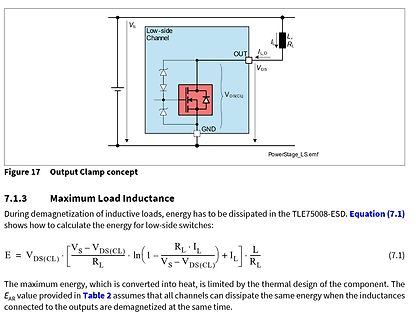
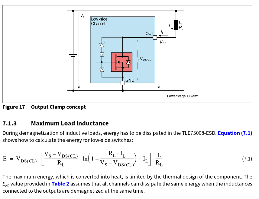
has to be dissipated in the TLE75008-ESD. Equation (7.1) shows how to calculate the energy for low-side switches:
E = VDS(CL) * [ (VS - VDS(CL)) / RL * ln(1 - IL * (VS - VDS(CL)) / RL) + IL ] * L / RL (7.1)
The maximum energy, which is converted into heat, is limited by the thermal design of the component

 Bild
Bild
 Bild
Bild
 Bild
Bild

 Bild
Bild
 Bild
Bild
 Bild
Bild
 Bild
Bild
 Bild
Bild
 Bild
Bild
 Bild
Bild
 Bild
Bild
 Bild
Bild
 Bild
Bild
 Bild
Bild
 Bild
Bild
 Bild
Bild
 Bild
Bild
 Bild
Bild
 Bild
Bild
 Bild
Bild
 Bild
Bild
 Bild
Bild