Descriptions Pin Pin No. Mnemonic Description No. Mnemonic Description 1 V SupplyVoltageforIsolatorSide1. 1 V SupplyVoltageforIsolatorSide1. DD1 DD1 2 V IA Logic Input A. 2 V OA Logic Output A. 3 V IB Logic Input B. 3 V IB Logic Input B. 4 GND 1 Ground1.GroundReferenceforIsolatorSide1. 4 GND 1 Ground1.GroundReferenceforIsolatorSide1. 5 GND 2 Ground2.GroundReferenceforIsolatorSide2. 5 GND 2 Ground2.GroundReferenceforIsolatorSide2. 6 V OB Logic Output B. 6 V OB Logic Output B. 7 V OA Logic Output A. 7 V IA Logic Input A. 8 V DD2
Foating Lead Protrusion is 0.15 mm (6 mils) max. Max. Lead Coplanarity * Maximum Mold flash on each side is 0.15 mm (0.006). = 0.102 (0.004) Broadcom AV02-2150EN 4 ACPL-064L, ACPL-M61L, ACPL-W61L, ACPL-K64L Data Sheet Low-Power 10-MBd Digital CMOS Optocouplers ACPL-W61L Stretched SO-6 Package *4.580 ±0.254
Foating Lead Protrusion is 0.15 mm (6 mils) max. Max. Lead Coplanarity * Maximum Mold flash on each side is 0.15 mm (0.006). = 0.102 (0.004) Broadcom AV02-2150EN 4 ACPL-064L, ACPL-M61L, ACPL-W61L, ACPL-K64L Data Sheet Low-Power 10-MBd Digital CMOS Optocouplers ACPL-W61L Stretched SO-6 Package *4.580 ±0.254
contact, including cutoff tab and burr, shall not be bent beyond the limitations given in Figure 4. Side-to-side — side-to-side bending of the contact may not exceed the limits provided in Figure 4. NOTE i Periodic inspections must be made to ensure crimped contact formation is consistent. Rev G2 5 of 11 114-2025 Up and Down Alignment 3° Max Datum Line 3° Max Side-to-Side Alignment 3° Max Datum Line 3° Max Figure 4 3.5. TensileInspection Crimped contacts should hold the wire firmly and have a pull-test tensile value meeting the values given in Figure 5. NOTE
inductor and the input bypass capacitor traces should be kept as short as possible. The positive side of the input capacitor should be close to the source of the P-channel MOSFET; it provides the AC current to the pass transistor. The connection between the diode and the pass transistor should also
- 4 External Locator - Top View with LCD Panel Open Introduction External Locator - Front & Right Side Views Figure 2 Front View 1. LED Indicators FRONT VIEW 1 . n r d u t Figure 3 n Right Side View 1. 2-In-1AudioJack RIGHT SIDE VIEW (Headphone and Microphone) 2. Microphone-In Jack 4 1 2 3 3. USB 2.0 Port 4. Vent External Locator - Front & Right Side Views 1 - 5 Introduction External Locator - Left Side & Rear View Figure 4 Left Side View 1. Security Lock Slot 2. RJ-45 LAN Jack 3. USB 3.2 Gen 2 / LEFT SIDE VIEW Type-A Ports 4. MicroSD Card Reader
spacing (mm) Fig 24. Inductance as a function of ground grid spacing Ideally, the top and bottom side of the PCB should look like a ground plane with horizontal ground traces on one side, and vertical ground traces on the other side. It is not absolutely necessary that the traces be orthogonal. The
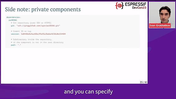
Side note: private components
dependencies:
pa1010d:
# Git repository (over SSH or HTTPS)
git: "ssh://git@github.com/igrr/pa1010d.git"
# Commit ID or tag
version: 5e0448e8e4ac88bc99a95a3bd6e4f58c0e154404
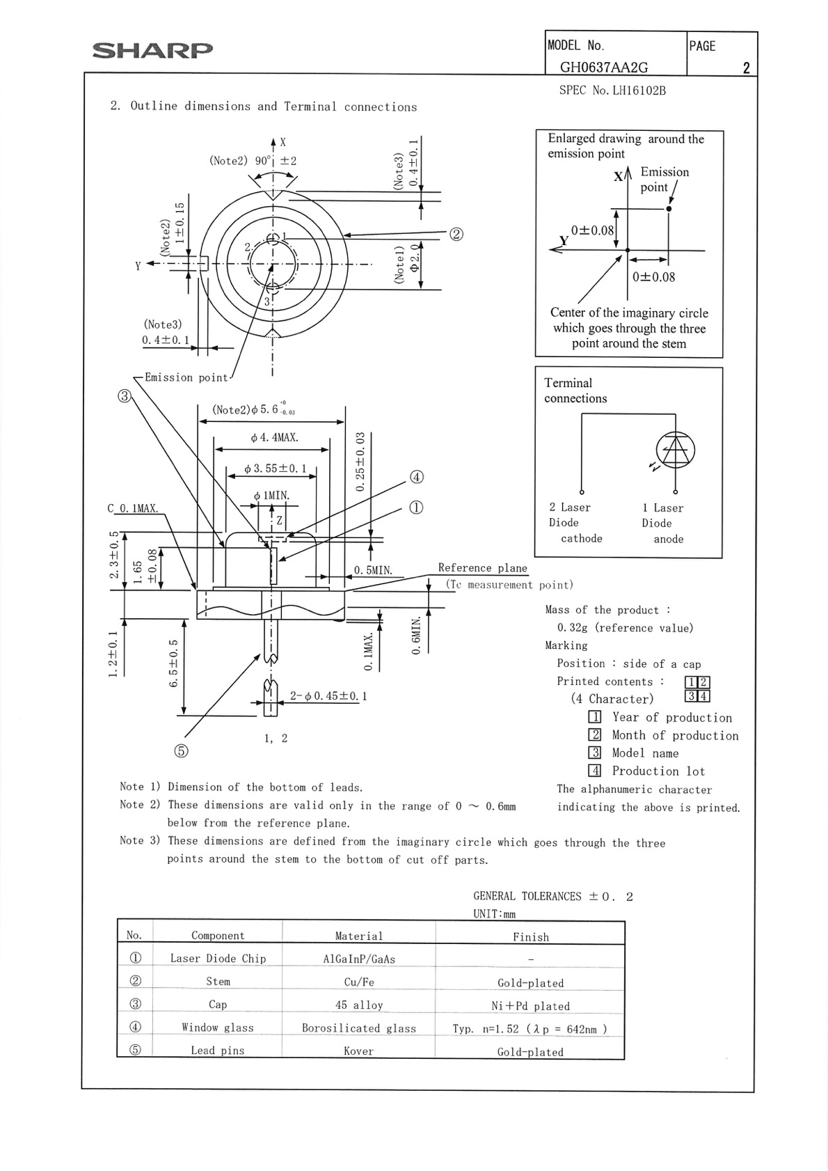
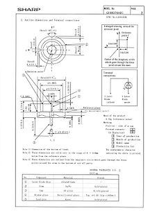
point) 0.5MIN. 0.1MAX. 0.6MIN. 5 Mass of the product : 0.32g (reference value) Marking Position : side of a cap Printed contents : 3 1 4 (4 Character) Year of production 2 Month of production 3 Model name 4 Production lot 1, 2 GENERAL TOLERANCES ± 0.2 UNIT:mm No. Component Material Finish 1 Laser Diode
einschalt-strombegrenzer-et-esb1-p262701.html?CCOUNTRY=445&LANGUAGE=en&GROUPID=9503&START=0&OFFSET=16&SID=92fab5f1aa1a8ee14123168df94531423bf482ec83ad922e40733&LANGUAGE=DE&&r=1 eine Appnote zu NTCs: https://www.tdk-electronics.tdk.com/download/528070/f5be4fca9d1f66204de9cf37891e5265/pdf-inrushcurrentlimiting-an2
enable_in : in std_logic; Real_in_from_ADC : in std_logic_vector(9 downto 0);--receiver side i/p imag_in_from_ADC : in std_logic_vector(9 downto 0); --receiver side i/p Dout1 : out std_logic_vector(9 downto 0);--receiver side 0/p Dout2 : out std_logic_vector(9 downto 0);--receiver side o/p CLK_out : out std_logic ; -- ADC_CLK2 : out std_logic; enable_out : out std_logic ); end entity; architecture behavioral of adc_interface is begin process(
J L P C I 228876fa 24 LTC2288/LTC2287/LTC2286 U U W U APPLICATIO S I FOR ATIO Silkscreen Top Top Side 228876fa 25 LTC2288/LTC2287/LTC2286 U U W U APPLICATIO S I FOR ATIO Inner Layer 2 GND Inner Layer 3 Power BottomSide 228876fa 26 LTC2288/LTC2287/LTC2286 U PACKAGE DESCRIPTIO UP Package 64-Lead Plastic QFN (9mm× 9mm) (Reference LTC DWG # 05-08-1705) 0.70 –0.05 7.15 –0.05 (4 SIDES) 8.10 –0.05 9.50 –0.05 PACKAGE OUTLINE 0.25 –0.05 0.50 BSC RECOMMENDED SOLDER PAD PITCH AND DIMENSIONS 9 .00 – 0.10 0.75 – 0.05 R = 0.115 (4 SIDES) TYP 63 64 0.40 – 0.10 PIN 1 TOP MARK (SEE NOTE 5)
bei einer wärmepumpe sid da hd- und nd-pressostaten verbaut. die lösen aus, wenn der arbeitsdruck zu niedrig oder auch zu hoch wird. und das signal bleibt dann auch stehen..
zusätzlich verkomplizieren. Bei nur 5x5x5 LEDs soll es doch vermutlich so funktionieren: Die High-Side der 25 LEDs einer Ebene werden alle jeweils über einen Pin am 74HC595 geschaltet. Die High-Side der LEDs jeder Ebene sind von oben nach unten durchverbunden. Die Low-Side der LEDs einer Ebene sind
Beitrag #7493505: > Bei nur 5x5x5 LEDs soll es doch vermutlich so funktionieren: > > Die High-Side der 25 LEDs einer Ebene werden alle jeweils über einen Pin > am 74HC595 geschaltet. Die High-Side der LEDs jeder Ebene sind von oben > nach unten durchverbunden. > > Die Low-Side der LEDs einer
created by adjacency heat theory. Simply, it means the center gets hotter because there is heat on both sides. The ends are cooler as there is only heat being generated from one side. To increase the current carrying ability of a long track, increase the surface area in the middle, increasing the heat dissipation
. (Note 3) W Maximum (Note 6) 0 B component Top 0 0.030 [0.75] rotation cover MIN. (Note 4) tape (Side or front sectional view) 0.004 [0.1] Center lines P For tape feeder MAX. of cavity 1 reference only D1MIN. for components USER DIRECTION OF FEED 0.079 x 0.047 [2.0 x 1.2] and larger. including draft
ESP32-S3. PCB-Antenne und Matching werde ich mit einem VNA noch durchführen. Verbaut: 8x SK6812-SIDE-A 1x AHT20 5x ALS-PT19-315 1x MCP73831T 1x MAX17048G+T10 1x ME6211C33M5G-N Ich habe das meiste in eigen Recherche versucht und hoffe das das ganze halbwegs solide ist. Das ganze soll entweder
MA1.6 NOTES: A2 1.35 1.40 r1.45 2. DIMENSIONS D1 AND E1 DO NOT INCLUDE b 0.13 0.16f o 0.23 0.25mm PER SIDE. D1 AND E1 ARE MAXIMUMIS D 0.09 16.00 BSC 0.20 3. DIMENSION b DOES NOT INCLUDE DAMBAR DE ti16.00 BSC SHALL NOT CAUSE THE LEAD WIDTH TO EXCEED Ee n 10.40 BSC 0.08mm.IMUM b DIMENSION BY MORE THAN L1 0e45
current by parallel connections. Master Slave 04 Dimensions [inch (mm)] Weight approx. 1.1 kg Top Front Side Rear 1.38(35) 0.87(22) 10.62(270) 0.16(4) 4.88(124) ▯-4 ▯-4 065 */ ▯▯▯▯▯▯▯▯▯"▯▯▯▯▯▯)[ 0.31(8) 4 × M3 Bottom 0.79(20) 1.04(26.5) 9.06(230) Load-off Timer Function As the load-off timer function is set
confidence not be reproducer or copied and not be used or incorporated in any product Light gray plastic side bumper Polished chrome side bumper 13120.30 13121.30 13122.30 13124.30 13120.47 13121.47 13122.47 13124.47 13120.23 13121.23 13122.23 13124.23 13120.44 13121.44 13122.44 13124.44 Proprietary and ConfidentialA
P0STLK0TX P0SB1401 P0SB1402 0 LD1 N Red 0 SB14 0 K O T T R21 L TX P CN3 T D I D R S Wired on Solder Side COM P0R2101 P0R2102D102 P RX 0 T T T 0 T R +3V3_ST_LINK C N J N N 0 N J 100 P STLINK_RXLINK0RX T T T T N T STLK_RX P0STLK0RX P0SB1301 P0SB1302 CN11 4 SB13 P0CN1101 P0CN1102 1 N0LED0STLINK R20 3P0LD103
side V OUT = 0 V T j< 85 °C – – 50 µA V INH= 0 V V OUT = 0 V T j= 150 °C 4.2.3 Reverse diode V DS(HS) V IOUT = -9 A forward-voltage high – 0.9 1.5 T j= -40 °C side 1) – 0.8 1.1 T = 25 °C j – 0.6 0.8 T j= 150 °C Low Side Switch - Static Characteristics 4.2.4 On state low side R ON(LS) mΩ IOUT = -9 A resistance V S= 13.5V – 9 12 T = 25 °C j – 14 18 T j= 150 °C 4.2.5 Leakage current low IL(LKLS) – – 1 µA V INH= 0 V side
idealen kilis von 8500 würdest du einen Is-Strom von 18µA erwarten. Der Leckstrom am Isense für High side Switch active ist schon worst case 200µA. Eine Halbbrücke die 43A abkann ist einfach nicht geeignet für dein Vorhaben. Bei einer kurzen Suche habe ich folgenden Kollegen gefunden: https://juergarnold.ch
frequency band according to your needs 39 | 75 FD6818 REV.1.0.0 Machine Translated by Google Key tone side tone BEEP and other settings Key tone side tone BEEP and other settings Key tone side tone on: WRITE(0x03,0x0202); //enable AF and Tx(PLL and PA are not include) WRITE(0x47,(REG_47H & 0xE0FF) | 0x1800
isolation between the transistors flags and the heatsink with digital ohm meter Fixing from down side: Fixing from up side: 5 1 2 3 4 C D A Motor- Motor + A DC Motor K1 P2 P3 P1 S-GND B Speed B Speed potentiometer or throttle +5V Forward NC C S-GND NO Reverse Direction switch Brake/PWM in RX TX C C
nehmen. Spricht bei meiner Messfrequenz etwas dagegen, die Brücke zwischen den Messungen über den Low Side Switch stromlos zu schalten, um Strom zu sparen?
dimensions do not include mold flash or protrusion. Mold flash and protrusion shall not exceed 0.25 per side. 4. Leads 1,2,3 may be wider than leads 4,5,6 for package orientation. 5. Refernce JEDEC MO-178. www.ti.com EXAMPLE BOARD LAYOUT DBV0006A SOT-23 - 1.45 mm max height SMALL OUTLINE TRANSISTOR PKG 6X
Ambient : Natural convection Soldering : Lead (Pb) free Board : Dimensions 40×40mm(1600mm 2 in one side) Copper (Cu) traces occupy 50% of the board area In top and back faces Package heat-sink is tied to the copper traces (Board of SOT-26 is used) Material : Glass Epoxy(FR-4) Thickness : 1.6mm Through-hole
, protrusions, or gate burrs. Mold flash, protrusions, or gate burrs shall not exceed 0.25 mm per side. 5. Support pin may differ or may not be present. www.ti.com EXAMPLE BOARD LAYOUT DBV0005A SOT-23 - 1.45 mm max height SMALL OUTLINE TRANSISTOR PKG 5X (1.1) 1 5X (0.6) 5 SYMM (1.9) 2 2X (0.95) 3 4 (
dimensions do not include mold flash or protrusion. Mold flash and protrusion shall not exceed 0.25 per side. 4. Leads 1,2,3 may be wider than leads 4,5,6 for package orientation. 5. Refernce JEDEC MO-178. www.ti.com EXAMPLE BOARD LAYOUT DBV0006A SOT-23 - 1.45 mm max height SMALL OUTLINE TRANSISTOR PKG 6X
connecting the driver in a common cathode configuration. This means that we connect all the negative sides of the control signal connections to ground. The connections are also given in the table below: TB6600 Connections 6/18 TB6600 Connection VCC 9 – 42 VDC GND Power supply ground ENA- Not connected ENA
...............................................................74 11.1 Valid Part Numbers and Top Side Marking........................................................................75 12. REVISION HISTORY................................................................................................
der Low-Side-FET zwischendurch immer auch mal kurz durchsteuert -> die PWM besser nie auf 100%. > Der Controller > arbeitet mit SPWM, also keine Blockkommutation, da kommt er nur kurz auf > max. 100%.
Blockkommuntierung, mit einem von der Steuerspannung abhängigen, festen Tastverhältnis auf den High-Side-FETs. Die Rampen, die man auf den Oszillogramm sieht, kann man an dem im jeweiligen Block gerade floatenden Spulenanschluss messen. Lass Dich von den Chinesen nicht verwirren! ;)
DESCRIPTION Top View Top View Pin # Symbol Function 1,2 GND Sense FET source terminal on primary side and internal control ground. 3 COMP Feedback input defines the peak drain MOSFET current. Positive supply voltage input. Although connected to an auxiliary transformer winding, current is supplied from
D B * The vibration-proof capacitors of size ø6.3 has support terminals extending from the bottom side to the lead edge. Then, make sure to find A E A appropriate soldering conditions to form fillet on the support terminals if required for appearance inspection. B Design and specifications are each subject
may flow in some of the capacitors. To prevent concentration of ripple current on the low-impedance side, use capacitors with the same product number and avoid the partiality of cable impedances. Do not use capacitors connected in series. ■ When the capacitor is mounted on a double-side wiring board, do
Meine Strategie wäre: 56 kOhm als ständige Pull-ups. Dazu per High-Side-Switch ca. 3,3 kOhm mit Software parallel schalten. Je nach erforderlicher Genauigkeit auch 3,1698113207547169811320754716981 kOhm... Nein, ernsthaft: 3,16 kOhm gibt' in der E48-Reihe und ist trivial zu beschaffen. (Die zum Idealwert fehlenden ca. 10 Ohm steuert sogar noch der High-Side-Switch teilweise bei.) 8-fach High-Side-Switches für SPI, also mit P-FET, sind auch leicht zu beschaffen. Irgendwann habe ich auch mal einen eingesetzt, weiß aber nicht mehr welchen. Nur 3 ICs
weil meßtechnisch nicht verifiziert, aber nach meinem Verständnis des Datenblatts werden die Low-Side-MOSFETs nicht gechoppert. Zitat aus Seite 22 des Datenblatts im Kapitel über den 1xPWM-Betrieb: The INLC input brakes the motor by turning off all high-side MOSFETs and turning on all low-side
über die Freilauf-Diode des High-Side-MOSFETs durchschlagen - trotz Sperrung. Ich verstehe nach wie vor nicht, warum eine etwaige Überspannung zwischen Low- und High-Side nicht sofort durch den Kurzschluß zwischen den Phasen zunichte
to the high-side power MOSFET source. SLA 8 8 I Low-side source sense input. Connect to the low-side power MOSFET source. SLB 9 9 I Low-side source sense input. Connect to the low-side power MOSFET source. SLC 16 16

 Bild
Bild
 Bild
Bild
 Bild
Bild
 Bild
Bild
 Bild
Bild