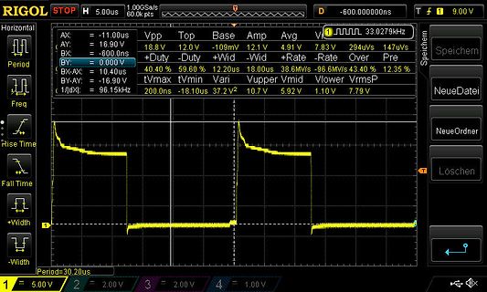
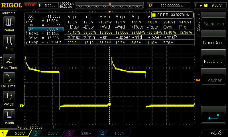
gewinnen (Osz. 32 MHz), wg. 50% Tastverhältnis (über 74AC74 teilen z.B.). Manche Bauteile wollten kein 40:60 oder 45:55.
dann denn sein, die Kurvenform aus 'nem digitalen IC? Ja: Rechteckig. Am Hameg 412 sah das vor 40 Jahren auch so aus und hat funktioniert. Wichtig ist aber: Tastkopf 1:10 verwenden (wurde bereits geschrieben).
established in 2011 and is located in Wenzhou City, Zhejiang Province. At present, the company has 40K sqm of modern manufacturing bases in Wenzhou and Wuhu with over 500 employees, including over 50 R&D and technical personnel. ETEK Electric has multiple production workshops for mold design, parts manufacturing
RATINGS DESCRIPTION SYMBOL BD433 BD435 BD437 BD439 BD441 UNIT BD434 BD436 BD438 BD440 BD442 Collector Base Voltage V CBO 22 32 45 60 80 V Collector Emitter Voltage V CES 22 32 45 60 80 V Collector Emitter Voltage V CEO 22 32 45 60 80 V Emitter Base Voltage V EBO 5.0 V Collector Current C 4.0 A Collector
antifreeze if heat pump systems are implemented in buildings tors. Use the plug connector located on the base of the heat where a power failure can not be detected (holiday home). pump adjacent to the cable gland in the base plate. More de- tailed information can be found in the operating instructions of the
/kWh beschissen fühlen. Dabei ist das wirtschaftlich betrachtet ein echtes Geschenk. Ich bezahl 40ct, bekomm aber nur 8ct. Den Geiern geb ich gar nichts, nicht mal wenn ichs wegschmeißen muss. So ist da glaub ich die Denke. Dabei sind von den 40ct schon mal 11ct Steuern und Abgaben an den Staat
Dieter D. schrieb im Beitrag #7714659: > Der durchschnittliche EPEX Base Preis lag 2023 bei 71,70 Euro/MWh, also > bei rund 7,17 ct/kWh und das liegt unter 8ct. Leider speisen Solaranlagen nicht so schön gleichverteilt über Tag und Jahr ein.
in any given applicationdepends on the user's specific board design. B. The power dissipatDonP is basJ(MAX)50°C, using ≤ 10s junction-to-ambient thermalresistance. C. Repetitive rating, pulse width limitedby junctioJ(MAX)0°C. Ratings are based on low frequency and duty cycles to keep initiJlT =25°C.
10 40 ns capacitive load of 400 pF] 20 80 ns tfDA fall time of SDAH signal capacitive load from 10 pF to 100 pF 10 80 ns capacitive load of 400 pF] 20 160 ns tSP pulse width of spikes that must be SDAH and
PC bzw. RX/TX bool digitalRead (pin) sin (rad) cos (rad) tan (rad) } * mal / geteilt sqrt (x) pow (base, exponent) begin (long speed)//bis 921600Bit/s void loop ( ) { % Modulo (Rest der GZ-Division) digitalWrite (pin, [HIGH, LOW]) int constrain(x, minval, maxval) begin (speed, config) //Config z.B. //
PC bzw. RX/TX bool digitalRead (pin) sin (rad) cos (rad) tan (rad) } * mal / geteilt sqrt (x) pow (base, exponent) begin (long speed)//bis 921600Bit/s void loop ( ) { % Modulo (Rest der GZ-Division) digitalWrite (pin, [HIGH, LOW]) int constrain(x, minval, maxval) begin (speed, config) //Config z.B. //
PC bzw. RX/TX bool digitalRead (pin) sin (rad) cos (rad) tan (rad) } * mal / geteilt sqrt (x) pow (base, exponent) begin (long speed)//bis 921600Bit/s void loop ( ) { % Modulo (Rest der GZ-Division) digitalWrite (pin, [HIGH, LOW]) int constrain(x, minval, maxval) begin (speed, config) //Config z.B. //
PC bzw. RX/TX bool digitalRead (pin) sin (rad) cos (rad) tan (rad) } * mal / geteilt sqrt (x) pow (base, exponent) begin (long speed)//bis 921600Bit/s void loop ( ) { % Modulo (Rest der GZ-Division) digitalWrite (pin, [HIGH, LOW]) int constrain(x, minval, maxval) begin (speed, config) //Config z.B. //
ich hab hier öfters "s-video" gelesen. Ist dann aber schon etwas anderes, als "FBAS" oder "BAS".
512MB RAM Mini HDMI port Micro USB OTG port Micro USB power HAT-compatible 40-pin header Composite video and reset headers <========= Unpopulated 40-pin GPIO connector CSI camera connector (need an adaptor cable) Compatible with Grove Base HAT to extent possibilities
Beitrag #7703616: > U=P/I Dann müssten die LEDs in Gruppen parallel geschaltet sein, denn 80W/2A = 40V. Und in 40V "passen" höchstens so um die 15 LED rein. Und wenn die LEDs sowohl in Reihe wie auch die Reihen parallel geschaltet sind, würde bei Ausfall eines Bonddrahtes nur eine der parallelen Gruppen
gibt dort ein vereinfachtes Datenblatt auf dessen Homepages. https://www.digikey.be/en/products/base-product/renesas-electronics-corporation/20/IW3623/318916 Das Prinzipschaltbild und das interne Prinzipschaltbild sind dort zu finden: https://www.renesas.com/us/en/products/power-power-management
− − V/µs Minimum trigger current IFT VD=6V, R L30Ω − − 8 mA 10 Isolation resistance R ISO DC500V, 40 to 60%RH 10 − − Ω Zero cross voltage V I =8mA − − 35 V OX F VD(rms)=100V, AC50Hz S116S02 − − 10 TransferTurn-on time ton T (rms)=2A, Resistance loadF I =20mA ms charac- VD(rms)=200V, AC50Hz teristics
- STP6NK60Z Package mechanical data TO-220 mechanical data mm inch Dim Min Typ Max Min Typ Max A 4.40 4.60 0.173 0.181 b 0.61 0.88 0.024 0.034 b1 1.14 1.70 0.044 0.066 c 0.49 0.70 0.019 0.027 D 15.25 15.75 0.6 0.62 D1 1.27 0.050 E 10 10.40 0.393 0.409 e 2.40 2.70 0.094 0.106 e1 4.95 5.15 0.194 0.202
43 müsste eine BAS40 sein. Kannst du bei dem anderen Bauteil relativ einfach gegen messen, ob das stimmt. Der 680 Ohm Widerstand ist auf jeden Fall auch mit hin. Tausche auch den Optokoppler mit, der hat es wahrscheinlich
Christian S. schrieb im Beitrag #7702520: > 43 müsste eine BAS40 sein. Sicher nicht. Das ist ein Digitaltransistor DTC143XKA von Rohm.
the ER● ● ● EC with ER GH housing and ER-AK, ER-AH or ER-AB with the ER EC fan insert. Air volume – base load 30 m³/h for continuous ope●ation ● ● ● Air volume of the base load and full load levels can be s●t ● ● Additional air volumes that can be set ● ●*** ● in base load: 20 m³/h, 40 m³/h, 60 m³/h or
- STP6NK60Z Package mechanical data TO-220 mechanical data mm inch Dim Min Typ Max Min Typ Max A 4.40 4.60 0.173 0.181 b 0.61 0.88 0.024 0.034 b1 1.14 1.70 0.044 0.066 c 0.49 0.70 0.019 0.027 D 15.25 15.75 0.6 0.62 D1 1.27 0.050 E 10 10.40 0.393 0.409 e 2.40 2.70 0.094 0.106 e1 4.95 5.15 0.194 0.202
LSIRD Internal low-speed oscillator ready Set and cleared by hardware to indicate if the internal RC 40 KHz oscillator is ready. After LSIEN is cleared, LSIRD goes low after 3 internal RC 40 KHz oscillator clock cycles. 0: Internal 40KHz RC oscillator clock not ready 1: Internal 40KHz RC oscillator clock
rating Tol. Pack-Code TCR Forming type R Value Special Power & Energy Computer & J = ±5% T = Tape - Base on52- Inner Taping UL = UL Version Peripherals (ammo pack) spec. dimension or YY = Standard 73- Inner Taping Automotive dimension ZB- Z version Historical VTM Part Nr.: CRF254 – 8 5 T 150R Precision
Collector-emitter VoltageBEV= 0) 32 45 V V CEO Collector-emitter VoltagB (I = 0) 32 45 V V EBO Emitter-base Voltage CI= 0) 7 V C Collector Current 200 mA I Base Current 50 mA B Ptot Total Power Dissipation atamb 25 ⋅C 0.39 mW at Tcase 45 ⋅C 1 W T stg Tj Storage and Junction Temperature – 65 to 200 ⋅C January
Treiber? Ich würde gern eine H-Brücke aufbauen, die in der Mitte eine Rechteckspannung von bis zu +/- 40V liefern kann bei +40V VDD. ich hatte dafür eigentlich den 4559 auserwählt... :-(
Hier wäre Literatur zur H-Brücke: https://www.homofaciens.de/technics-base-circuits-h-bridge_ge.htm Noch ein paar Beispiele: https://blasted.de/threads/mosfet-aktive-motorbremse-active-breaking-system.5645/ https://www.arduinoforum.de/attachment.php?aid=7216
Replace Display PCB. PCB? Main PCB 38 Vibration & Noise During Spin Have all the Transit Bolts and the Base Packing NO Remove the Transit Bolts and been removed? the Base Packing. Washer Base Packing Packing Support YES Refer to INSTALLATION. (Page 8) 39 Detergent & Softener does not flow in Is water supplied
Geschwindigkeit fällt linear. [code] a_mm=47.8; % Durchmesser Rotor b_mm=20;% Laenge Pol m_g=40; % Gewicht Rotor a=a_mm/1000; b=b_mm/1000; m=m_g/1000; # Trägheitsmoment J=1/12*m*(a*a+b*b) format short eng disp(J) decelaration_RPM_per_sec=(1592-344)/4 decelaration_rounds_per_sec2=
scope at /home/christoph/Entwicklung/Modell/modelJulia.jl:15 [2] include(::Module, ::String) at ./Base.jl:377 [3] exec_options(::Base.JLOptions) at ./client.jl:288 [4] _start() at ./client.jl:484 in expression starting at /home/christoph/Entwicklung/Modell/modelJulia.jl:15 [/c] Hast Du einen
2V710 Capacitor Non-Polar Radial Electrolytic 100UF 16V C322 2P910AM Capacitor Radial Electrolytic Dia 40mm PCB Mount 10000uF 71V C323 2P910AM Capacitor Radial Electrolytic Dia 40mm PCB Mount 10000uF 71V D101 3AS16W Diode Surface Mount Small Signal BAS16W SOT-23 Package D200 3AS16W Diode Surface Mount Small Signal BAS16W SOT-23 Package D201 3AS16W Diode Surface Mount Small Signal BAS16W SOT-23 Package D202 3AS16W Diode Surface Mount Small Signal BAS16W SOT-23 Package D203 3AV99W Diode Dual Surface Mount Small Signal
Ambienttemperatureoperation(°C) 55 55 55 55 55 55 55 55 55 m r n Ambienttemp. duringstorage/transport(°C) -40 to 85 -40 to 85 -40 to 85 -40 to 85 -40 to 85 -40 to 85 -40 to 85 -40 to 85 -40 to 85 E e IP Class 20 20 20 20 20 20 20 20 20 s l n E Weight (kg) 0.27 0.34 0.28 0.32 0.31 0.31 0.26 0.26 0.43 Connectors
1970/1 31 - 37 Measuring A Calibration Spectrum Generator for Two Meters H Gotting, DL3XW 1970/1 38 - 40 Technology 2 m Band Modification of the DJ9ZR 001 5 W SSB Transmitter H U Beitz, DJ8XR 1970/1 40 2 m Band A Transistorised Calibration Spectrum Generator for Two Meters H Gotting, DL3XW 1970/1 41 - 44
Transientanalyse sieht man nun 20kHz in eine 300Ohm Last. Der Ruhestrom liegt allerdings so bei um die 40mA. Im Grunde ist die Designaufgabe damit erfüllt. Bei der Bipolaren Vorstufe bin ich nicht ganz sicher wie das gemeint ist. Ich bin mir gerade unsicher wie ich diese an die VAS Stufe bringen soll
fließt, dann ist auch kein Offset da. Das gilt natürlich nur, wenn auch die DC-Widerstände an den Basen des Diff gleich groß sind, was bei dir auch nicht gegeben ist (3k3 <-> 5k).
POF with 0.22 dB/m typical attenuation • Every plastic fiber with an external diameter of 2.2 mm (-40°C to 85°C) and an internal diameter of 1 mm can be used - High performance Extra Low Loss POF with 0.19 dB/m • Small housing dimensions typical attenuation (-40°C to 85°C) • The housing protects photodetectors
meiner Anwesenheit?) natürlich zu keinem Ausfall. Aber u.s.w., mal ein Blick auf die Seite 40 der Anleitung dort: https://static.ggmgastro.com/K%C3%BChlung/kuehlschrank/kgi%26tgi/KGI%20TGI%20Anleitung%20DE.pdf Auf dem rechten Bild erkenne ich, dass die Medium-Leitungen des
#7682551 Du sagst "kein zu harter Pinsel" und der Hersteller sagt "Bürste mit harten Borsten" (Siehe S.40). Ich denke, der Hersteller kennt sein Produkt.
Load BIOS Defaults F7 : Load Setup Defaults Figure 4.4: CHIPSET FEATURES SETUP • EDO,60nsDR AM or 40MHz CLK The default value is Disabled. Enabled EDO DRAM or 60ns DRAM or 40MHz CLK Present. ¡ ] DX-40, DX2-80, DX4-120¡ ^ Disabled EDO DRAM or 60ns DRAM or 40MHz CLK Absent. ¡ ] DX-40, DX2-80, DX4-120¡
apps). For brevity, we only illustrate results for the 40 apps that 5 MOBILE APP I/O CHARACTERIZATION displayed the highest average I/O throughput. Surprisingly, the A goal of this work is to defend against premature wear-out and most write-I/O-heavy app was
Range: 0°C to +70°C Fully Compliant with IEEE 802.3/802.3u Stan- • Industrial Temperature Range: –40°C to +85°C dards • Available in 32-pin (5 mm x 5 mm) QFN Package • SPI with Clock Speeds up to 40 MHz for High Additional Features Throughput Applications • Supports 10BASE-T/100BASE-TX In addition to
. Ich hab sogar emv Messungen mit dem Design gemacht, da lagen Welten dazwischen. Oder in dem Fall 40dB.
Ich hab sogar emv Messungen mit dem > Design gemacht, da lagen Welten dazwischen. Oder in dem Fall 40dB. Und was ist die Erklärung für den Effekt? Allgemeingültig ist das mal sicher nicht (Hallo Lothar).
sollte das aber die Beschaltung weiter oben bestätigen. Und das meine ich ja auch. Mein SFP kostet 40€. Ein Fehltritt wäre halt nicht so günstig, aber ich werde es wohl mal versuchen, nachdem ich mir die neue Spezifikation durchgelesen habe. Vielen Dank dafür! Beste Grüße
Kai S. schrieb im Beitrag #7677082: > Mein SFP kostet 40€. Du meinst ganz sicher SFP, und nicht SFP+? Wenn 5 m reichen, sind DAC-Kabel eine Alternative.
transceiver vendor name (ASCII) 36 1 Reserved 37-39 3 Vendor OUI SFP transceiver vendor IEEE company ID 40-55 16 Vendor PN Part number provided by SFP transceiver vendor (ASCII) 56-59 4 Vendor rev Revision level for part number provided by vendor (ASCII) 60-62 3 Reserved 63 1 CC_BASE Check code for Base ID
ing boards. (at 4 sigma) 60 µm (6-Nozzle Collect & Place Head) While the PCB is transferring from 40 µm (Pick & Place Head) the buffer zone to the stationary PCB dimensions (L x W) population zone, the Collect & Single conveyor 50 x 50 mm 2to 508 x 460 mm /2 Place Head is already picking up 2" x 2"
Considerations: ● 10/100/1000 relates to the data rate in Mbps (i.e. 10Mbps, 100Mbps, and 1000Mbps) •For 10 Base-T, data is transmitted over 2 UTP (unshielded twisted pairs) using a 10MHz clock •For 100 Base-TX, data is transmitted over 2 UTP using a 125MHz clock •For 1000 Base-T data is transmitted over 4 UTP
offset stack .equ 0xffbf ; Stack adr_vec_table .equ offset+0x40 ; Mode 2 Vektor Tabelle für STI Mostek Multi I/O adr_copyright .equ offset+0x80 heap_size .equ 2048 ; Benutzer definierte Heap Groesse ; Globale Funktionen und
The principal entry point to the FDOS is at location BOOT+0005H (normally 0005H) where a jump to BASE is found. As mentioned above, access to the FDOS functions is accomplished by passing a function number and information address through the primary point at location BOOT+0005H Danke, das reicht
Voltage VCC 0 3.6 Vdc CPx, Reset, Data In, Data Out VoltagVCP -0.3 V CC+0.05 Vdc Operating Temperature -40 85 oC o Storage Temperature -40 85 C Table 2-5 Recommended Operating Conditions Parameter Symbol Min Typical Max Units Supply Voltage VCC 3.15 3.3 3.46 Vdc Supply Voltage Ripples VCC_PP 2 % 100Base-TX Active CC 225 270 mA (Evolution) 100Base-TX Active (Linux) I 200 270 mA CC 100Base-TX Idle (Evolution) CC 215 mA 100Base-TX Idle (Linux) CC 175 mA 10Base-T Active (Evolution) I 145 250 mA CC 10Base-T Active (Linux) CC 130 250 mA xPort® Pro
pegainuerassoipùdue oi,mon- ttiuuna atiadicrutostampaota cnssmallatna,ermnnizae eprie RFecon unotloi40cm iRFeneäprpiopc!. 1; AYH. figura 1 E G I r di Per isemiconduttori e la bobina vedi testo. L'impedenza RF(Geloso 556). . L_ 1E: Irma, 0C171iie,unina comieaoe nsuerazoe, n untdo lsscsio, chi ä pr)rieaomoltoniie
= –40 mA 6 9.5 Ω RON(flat)) ON-state resistance All I/O VCC = 3 V, VI/O 1.5 V and VCC, 1.5 Ω flatness I/O= –40 mA On-state resistance match VCC = 3 V, 1.5 V ≤ I/O≤ VCC, ΔR ON(4) between high-speed D0 to D3

 Bild
Bild
 Bild
Bild