-
PDF
2N7000.pdf
Figure 21. Switching time waveform b O V(BR)DSS ton off tdon tr toff tf VD IDM 90% 90% 10% D 0 10% V DS VDD VDD 90% V GS AM01472v1 0 10% AM01473v1 9/14 Package mechanical2N7000, 2N7002 4 Package mechanical data packages. These packages have a Lead-free second level interconnect. The category of conditions
in „Schaltung mit 2 N-Kanal Mosfet“ · Analoge Elektronik und Schaltungstechnik ·
-
PDF
DS1220Y.pdf
ofCC . 12. WR1 , DH1 are measured from WE going high. 13. WR2 , DH2 are measured from CE going high. 14. DS1220Y modules are recognized by Underwriters Laboratories (UL) under file E99151 (R). DC TEST CONDITIONS AC TEST CONDITIONS Outputs open. Output Load: 100pF + 1TTL Gate All voltages are referenced
in „[S] DALLAS DS1220Y-150 NVRAM (NOS)“ · Analoge Elektronik und Schaltungstechnik ·
-
Datei
Startup.S
Mode */ /* R14 = LR */ ldr r14, =VIC_base_addr ldr r0 , [r14, #VIC_vect_offs] /*str r14, [r14, #VIC_vect_offs]*/ /*- Enable Interrupt and Switch in Supervisor Mode */ msr CPSR_c, #Mode_SVC /*- Save scratch/used registers
in „modify stack start in linker file of an LPC2148 project“ · µC & Digital Electronics ·
-
Datei
Startup.S
Mode */ /* R14 = LR */ ldr r14, =VIC_base_addr ldr r0 , [r14, #VIC_vect_offs] /*str r14, [r14, #VIC_vect_offs]*/ /*- Enable Interrupt and Switch in Supervisor Mode */ msr CPSR_c, #Mode_SVC /*- Save scratch/used registers
in „Interrupt beim ARM“ · Mikrocontroller und Digitale Elektronik ·
-
PDF
sla7024m.pdf
Symbol Test Conditions Min Typ Max Units FET Leakage Current I V = 100 V, V = 44 V — — 4.0 mA DSS DS CC FET ON Voltage V (SLA7024M & SMA7029M) V = 14 V, I = 1 A — — 600 mV DS(ON) CC OUT (SLA7026M) V CC = 14 V, IOUT = 3 A — — 850 mV FET ON Resistance r (SLA7024M & SMA7029M) V = 14 V, I = 1 A — — 600 mΩ DS(on) CC OUT (SLA7026M) V = 14 V, I = 3 A — — 285 mΩ CC OUT Body Diode V SD (SLA7024M & SMA7029M) I OUT = –1 A — 0.9 1.5 V Forward Voltage (SLA7026M) I = –3 A — 0.9 1.6 V OUT Control Supply Voltage V Operating
-
PDF
70599B.pdf
Analog-for-the-Digital Age, Application Maestro, CodeGuard, arising from this information and its use. Use of Microchip dsPICDEM, dsPICDEM.net, dsPICworks, dsSPEAK, ECAN, devices in life support and/or safety applications is entirely at ECONOMONITOR, FanSense, HI-TIDE, In-Circuit Serial the buyer’s risk, and the buyer agrees
in „AVR32UC3B mit Funkmodul MRF24J40MB“ · Mikrocontroller und Digitale Elektronik ·
-
 Bild
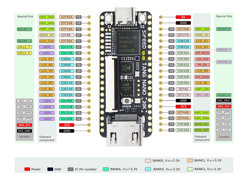
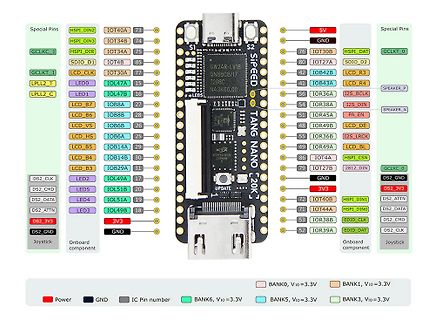
Pinbelegung einer Tang Nano 20K FPGA-Entwicklungsplatine
, I2S_DIN, LCD_B6, IOB8B, 28, 56, IOR36A, LCD_BL, LCD_VS, IOB6B, 26, 51, IOR45A, PA_EN, LCD_B5, IOB14A, 29, 48, IOR49B, LCD_DE, LCD_B4, IOB14B, 30, 55, IOR36B, I2S_LRCK, LCD_B3, IOB29A, 31, 49, IOR49A, LCD_BL, 86, IOL4AA, HSPI_CSN, 79, IOT27B, 2812_DIN, GCLKC_0, DS2_CLK, LED2, IOL49A, 17, GND, DS2_GND, DS2_CMD, LED5, IOL51B, 20, 3V3, DS2_ATTN, DS2_DATA, LED4, IOL51A, 19, 72, IOT40B, HSPI_DIN1, DS2_ATTN, DS2_3V3, LED3, IOL49B, 18, 71, IOT44A, HSPI_DIN0, DS2_DATA, DS2_GND, DS2_CLK, Tang Nano 20K, UPDATE
in „Neuigkeiten von Flash und MRAM, neue Boards für Entwickler“ · Mikrocontroller und Digitale Elektronik · · Screenshots
-
PDF
40001722A.pdf
. DS40001722A-page 2 Preliminary 2013 Microchip Technology Inc. PIC16(L)F1703/7 Pin Diagrams FIGURE 1: 14-PIN DIAGRAM FOR PIC16(L)F1703 PDIP, SOIC, TSSOP 1 14 V SS VDD RA5 2 3 13 RA0/ICSPDAT RA4 3 7 12
in „PIC16(L)F1703 low voltage Programmierung?“ · Mikrocontroller und Digitale Elektronik ·
-
Datei
riglol.c
("\n"); printf("DS2000 and DS4000 device options:\n"); printf(" first character: D = official, V = trial\n"); printf(" second character: S\n"); printf(" third character: A = DS2000, H = DS4000\n"); printf(" last character
in „Rigol-DS1054Z“ · Mikrocontroller und Digitale Elektronik ·
-
PDF
01006a.pdf
11 21 22 23 24 25 26 27 28 29 30 31 SCK instruction 16-bit address data byte SI 0 0 0 0 0 0 1 0 15 14 13 12 2 1 0 7 6 5 4 3 2 1 0 high-impedance SO DS01006A-page 4 © 2005 Microchip Technology Inc. AN1006 DATA POLLING (RDSR – CHECK FOR WIP SET) After a valid write command is given, the STATUS register
in „Infineon µC XC164D-Serie“ · Mikrocontroller und Digitale Elektronik ·
-
PDF
MCP2551.pdf
voltage 0V Receive data output voltage 0.3 VDD 11 VRS = 4V; TXD = 2V © 2007 Microchip Technology Inc. DS21667E-page 13 MCP2551 NOTES: DS21667E-page 14 © 2007 Microchip Technology Inc. MCP2551 3.0 PACKAGING INFORMATION 3.1 Package Marking Information 8-Lead PDIP (300 mil) Example: XXXXXXXX MCP2551 XXXXXNNN
in „CAN-BUS - Nur empfangen - Was mache ich mit dem TXD Pin am Tranceiver??“ · Mikrocontroller und Digitale Elektronik ·
-
PDF
CS4272.pdf
19 AINB- SCL/CCLK 11 18 AINB+ SDA/CDIN 12 17 AINA+ AD0/CS 13 16 AINA- RST 14 15 VCOM 6 DS593PP3 CS4272 Pin Name # Pin Description XTO 1,2 Crystal Connections (Input/Output) - I/O pins for an external crystal which may be used to generate XTI MCLK. See “Crystal Applications (XTI
in „was ist "ATAPI channel mixing" Warum kein Ausgangssignal?“ · Mikrocontroller und Digitale Elektronik ·
-
PDF
FT2232_datasheet.pdf
opposed to a USB 2.0 (n+0.375), (n+0.5), (n+0.625), (n+0.75) and (n+0.875) High Speed device (480Mb/s). 14 where n is an integer between 2 and 16,384 (2 ). DS2232D Version 0.91 © Future Technology Devices International Ltd. 2006 Page of 51 FT2232D Dual USB UART / FIFO I.C. In addition to the BM chip features
in „AVR-Programmierung via USB mit FT2232“ · Mikrocontroller und Digitale Elektronik ·
-
PDF
IRF3205S.pdf
Temperature www.irf.com 3 IRF3205S/IRF3205L 6000 V = 0V, f = 1 MHZ 16 I = 62A GS D Ciss= Cgs + Cgd, ds SHORTED V 14 V DS= 44V 5000 Crss = Cgd ( V DS= 27V C = C + C g V DS= 11V ) oss ds gd l 12 F4000 o e Ciss V 10 n r i u c3000 S 8 p o C - 6 ,2000 Coss a C G , 4 1000 G Crss V 2 0 0 1 10 100 0 20 40 60
in „Mosfet Treiber TC4426 + IRF IRF3205S (Ersatz gesucht)“ · Analoge Elektronik und Schaltungstechnik ·
-
PDF
DS18B20.pdf
DS18B20. If the line is low, a 0 is written to the DS18B20. READ/WRITE TIME SLOT TIMING DIAGRAM Figure 14 START OF SLOT OF SLOT MASTER WRITE “0” SLOT MASTER WRITE “1” SLOT 1μs < REC<∞ 60μs < TX“0” < 120μs
in „Suche nach einem Temperatursensor“ · Mikrocontroller und Digitale Elektronik ·
-
PDF
DS18B20.pdf
DS18B20. If the line is low, a 0 is written to the DS18B20. READ/WRITE TIME SLOT TIMING DIAGRAM Figure 14 START OF SLOT OF SLOT MASTER WRITE “0” SLOT MASTER WRITE “1” SLOT 1μs < REC<∞ 60μs < TX“0” < 120μs
in „Mehrere DS18B20 an einen Pin Avr-Mega32“ · Mikrocontroller und Digitale Elektronik ·
-
PDF
AN-9010.PDF
than O and when it is in a state where the F is t ~ t being conducted, V maintains the V . Figure 14 shows 3 4 DS DD t3~ t4is the period where it operates in an ohmic region. the voltage a little less than DD . This is caused by the The V increases up to V with a time constant of voltage drop due to the existing inductance in the line. GS GG t2= R GC +gs gd2). Figure14 shows the V GS (t) measuring the Va variation in accordance with i conditions in turn−on state. Drain−Source On Resistance (R ) D DS(on) VGS(t) ÉÉÉÉÉÉÉÉÉÉÉÉÉÉÉÉ O = 10 [A] 10 [V] IO= 7 [A] ÉÉÉÉÉÉÉÉÉÉÉÉÉÉÉÉ
in „SMD Mosfet mit Z-Diode für induktive Last“ · Analoge Elektronik und Schaltungstechnik ·
-
PDF
BSS169.pdf
specified Parameter Symbol Conditions Value Unit Continuous drain current ID TA=25 °C 0.17 A TA=70 °C 0.14 I T =25 °C Pulsed drain current D,pulse A 0.68 I =0.17 A, V =80 V, D DS Reverse diode dv/dt dv/dt di/dt=200 A/µs, 6 kV/µs Tj,max150 °C Gate source voltage V GS ±20 V ESD sensitivity (HBM) as per Class
in „Strombegrenzung mit Fet um Akku zu laden“ · Analoge Elektronik und Schaltungstechnik ·
-
PDF
3703fc.pdf
0.5 1.2 1.0 0 0 –50 –25 0 25 50 75 100 125 150 –50 –25 0 25 50 75 100 125 150 5 6 7 8 9 10 11 12 13 14 15 TEMPERATURE (°C) TEMPERATURE (°C) DRV CCOOST VOLTAGE (V) 3703 G10 3703 G11 3703 G12 Driver Pull-Down R DS(ON) vs Rise/Fall Time vs Gate RUN/SS Pull-Up Current vs Supply Voltage Capacitance Temperature
in „Längs- oder Querregler 40V 250W als Überspannungsschutz für Tiefstellsetzer“ · Analoge Elektronik und Schaltungstechnik ·
-
PDF
mdlm7301.pdf
otherwise specified Supply Current vs VOS vs VOS vs V CM Supply Voltage Supply Voltage V = ± 1.1V S DS012842-3 DS012842-4 DS012842-5 V OS vs VCM VOS vs VCM Inverting Input, V = ± 2.5V V = ± 15V S S Bias Current vs Common Mode Voltage V = ± 1.1V S DS012842-6 DS012842-7 DS012842-8 5 www.national.com = =
in „Problem mit OP als Spannungsfolger vor ADC“ · Analoge Elektronik und Schaltungstechnik ·
-
PDF
Datenblatt_DS18B20.pdf
DS18B20. If the line is low, a 0 is written to the DS18B20. Figure 14. Read/Write Time Slot Timing Diagram START OF SLOT OF SLOT MASTER WRITE “0” SLOT MASTER WRITE “1” SLOT 1μs < T <∞ REC 60μs < TX“0” <
in „DS18B20 Darstellung von negativen Zahlen im Zweierkomplement?“ · Mikrocontroller und Digitale Elektronik ·
-
PDF
Datenblatt_DS18B20.pdf
DS18B20. If the line is low, a 0 is written to the DS18B20. Figure 14. Read/Write Time Slot Timing Diagram START OF SLOT OF SLOT MASTER WRITE “0” SLOT MASTER WRITE “1” SLOT 1μs < T <∞ REC 60μs < TX“0” <
in „Timing Probleme 1-Wire“ · Mikrocontroller und Digitale Elektronik ·
-
PDF
Datenblatt_DS18B20.pdf
DS18B20. If the line is low, a 0 is written to the DS18B20. Figure 14. Read/Write Time Slot Timing Diagram START OF SLOT OF SLOT MASTER WRITE “0” SLOT MASTER WRITE “1” SLOT 1μs < T <∞ REC 60μs < TX“0” <
in „1-Wire Protokollablauf“ · Mikrocontroller und Digitale Elektronik ·
-
PDF
irlr3717.pdf
––– See Fig. 16 Q Switch Charge (Q + Q ) ––– 9.1 ––– sw gs2 gd Q oss Output Charge ––– 13 ––– nC V DS= 10V, VGS= 0V td(on) Turn-On Delay Time ––– 14 ––– V DD= 10V, VGS= 4.5V e t r Rise Time ––– 14 ––– ns ID= 12A td(off) Turn-Off Delay Time ––– 5.8 ––– Clamped Inductive Load tf Fall Time ––– 16 ––– C
-
PDF
CW6626-Datasheet-DS6626V1.1.pdf
............................................................... 14 2.6.3. PLL. ............................................................................................................................... 14 2.7. Power Management ..................................
-
PDF
_PIC16F176X-7X.pdf
PIC16(L)F1773/6 Data Sheet, DS40001810 CPU High-Endurance Flash Data Gemory-bit & 10-bit DAC (Up to 4 each) 149 Total Instructionsth 100 K Erase / Write CycLes High-Speed ■■ PIC16(L)F1777/8/9 Data Sheet, DS40001819 A Comparators (Up to 8) A ■■ Focus Product Selector Guide, DS00001308 (Up to 100 mA)/Os ■■ Quick Guide to Microchip Development Tools, BOR, WDT, LBPOR, POR, XLP DatUp to 2 KBRAM) Op Amps (Up to 4) DS50001894 Ramp Generator (Up to 4) Links DIGITAL PERIWith PERIPHERAL
in „Wie im Bereich von 1,2Vdc - 117Vdc einstellbare Konstantspannung aus 20Vdc erzeugen?“ · Mikrocontroller und Digitale Elektronik ·
-
PDF
bs208.pdf
DC) open drain − − ±20 V Y forward transfer admittance I = −200 mA; V = −25 V 100 200 − mS fs D DS D drain current (DC) − − −0.2 A RDS(on) drain-source on-state resistanGS = −10 V;DI = −200 mA − 10 14 Ptot total power dissipation Tamb = 25 °C − − 0.83 W April 1995 2 Philips Semiconductors Product
in „Mosfet BS208 sperrt nicht bei >3V“ · Analoge Elektronik und Schaltungstechnik ·
-
PDF
FDW2501NZ.pdf
V GS= 0 V, D = 250 µA 20 V Z ∆BV DSS Breakdown Voltage Temperature I = 250 µA, Referenced to 25°C 14 mV/°C ∆T J Coefficient D DSS Zero Gate Voltage Drain Current V DS= 16 V, V GS= 0 V 1 µA GSSF Gate–Body Leakage, Forward V GS= 12 V, V DS= 0 V 10 µA GSSR Gate–Body Leakage, Reverse V GS= –12 V, V DS= 0 V –10 µA On Characteristics (Note 2) VGS(th) Gate Threshold Voltage V DS= V GSID= 250 µA 0.6 1.0 1.5 V ∆VGS(th) Gate Threshold Voltage ID = 250 µA, Referenced to 25°C –3 mV/°C ∆T J Temperature Coefficient RDS(on) Static Drain–Source V GS= 4.5 V, D = 5.5 A 14 18 mΩ On–Resistance
in „N-Fet leitet auch bei 0v Gate-Spannung?“ · Mikrocontroller und Digitale Elektronik ·
-
Datei
RFM70_HH.c
, RX_ptr,0); status = SPI_send_get(FLUSH_TX, TX_ptr, RX_ptr,0); status |= STATUS_RX_DR | STATUS_TX_DS | STATUS_MAX_RT; // clear RX_DR or TX_DS or MAX_RT interrupt flag SPI_send_get(WRITE_REG|STATUS, &status, RX_ptr,1); // update status reg RFM70_disable; if (mode) status = MASK_RX_DR | EN_CRC | CRCO
in „RFM70 arbeitet nicht zuverlässig“ · HF, Funk und Felder ·
-
PDF
MCP23017-Datasheet.pdf
OP W DIN .... DIN P P S OP R DOUT ....DOUT P SR OP R DOUT ....DOUT P D SR OP W ADDR IN .... DIN P P DS20001952C-page 14 2005-2016 Microchip Technology Inc. MCP23017/MCP23S17 3.2.3 SPI INTERFACE four fixed bits and three user-defined hardware address bits (pins A2, A1 and A0). Figure 3-4 shows 3.2.3.1
in „kennt jemand sich aus mit MC23017 IO-Board“ · Mikrocontroller und Digitale Elektronik ·
-
PDF
ds1820.pdf
GND T = T = Master samples small small 15ms LINE TYPE LEGEND Bus master pulling low Resistor pullup 14 of 21 DS18S20 ROM COMMANDS FLOW CHART Figure 14 Initialization MASTER T X RESET PULSE Sequence DS18S20 X PRESENCE PULSE MASTER TXROM COMMAND 33h N 55h N F0h N ECh N CCh N READ ROM MATCH ROM SEARCH ROM
in „Thermometer mit ds18s20 und LED Annzeige“ · Projekte & Code ·
-
PDF
DS1820-DS1820S.pdf
GND T = T = Master samples small small 15 µ LINE TYPE LEGEND Bus master pulling low Resistor pullup 14 of 21 DS18S20 ROM COMMANDS FLOW CHART Figure 14 Initialization MASTER T X Sequence RESET PULSE DS18S20 X PRESENCE PULSE MASTER TXROM COMMAND 33h N 55h F0h N ECh N CCh READ ROM MATCH ROM N SEARCH ROM
in „1-Wire & Pull-UP“ · Mikrocontroller und Digitale Elektronik ·
-
PDF
DS18B20.pdf
to the DS18B20. If the line is low, a 0 is written to the DS18B20. READ/WRITE TIME SLOT TIMING DIAGRAM Figure 14 START OF SLOT OF SLOT MASTER WRITE “0” SLOT MASTER WRITE “1” SLOT 1ms < REC< ¥ 60ms < X “0” < 120ms
-
PDF
DS18b20.pdf
to the DS18B20. If the line is low, a 0 is written to the DS18B20. READ/WRITE TIME SLOT TIMING DIAGRAM Figure 14 START START OF SLOT OF SLOT MASTER WRITE “0” SLOT MASTER WRITE “1” SLOT 1 µ < TREC<∞ 60µs < X “0
in „Temperatur ohne AD-Eingang messen“ · Mikrocontroller und Digitale Elektronik ·
-
PDF
DS18b20.pdf
to the DS18B20. If the line is low, a 0 is written to the DS18B20. READ/WRITE TIME SLOT TIMING DIAGRAM Figure 14 START START OF SLOT OF SLOT MASTER WRITE “0” SLOT MASTER WRITE “1” SLOT 1 µ < TREC<∞ 60µs < X “0
in „Displaybeleuchtung faden ohne Analog I/O“ · Mikrocontroller und Digitale Elektronik ·
-
Datei
LCD_PCF8574-dotmatrix_7219--learn.asm
arbeitsregister .def IRQ_index = r22 ;IRQ-zähler .def testindex = r23 .equ DQ = 7 ;Datenleitung des Ds18B20 .equ DS_DDR = DDRC ;Data Direction Port des DS18B20 .equ DS_Port = PortC ; .equ DS_Pin = PinC ; .equ XTAL = 4000000 ;Quartzfrequenz .equ BAUD = 9600 ;Baudrate für UART .equ EEProm = 0xAE .equ RTC
-
PDF
SPP80N06S2L-07.pdf
R f 4.5 14 100 e g 5.0 h 10.0 12 80 10 d f 60 8 g c 6 h 40 b 4 VGS[V] = 20 a b c d e f g h 2 3.23.5 3.8 4.0 4.55.0 10.0 0.0 0.5 1.0 1.5 2.0 2.5 3.0 3.5 4.0 V 5.0 00 20 40 60 80 A 120 V I DS D 7 Typ. transfer characteristics
in „Transistor (Mosfet) Temperatur“ · Analoge Elektronik und Schaltungstechnik ·
-
PDF
A300_25AA640A_25LC640A-MIC.pdf
in LSB in High-Impedance SO FIGURE 1-3: SERIAL OUTPUT TIMING CS 9 10 3 Mode 1,1 SCK Mode 0,0 13 15 14 SO MSB out ISB out Don’t Care SI © 2008 Microchip Technology Inc. DS21830D-page 5 25AA640A/25LC640A 2.0 FUNCTIONAL DESCRIPTION 2.1 Principles of Operation 2.3 Write Sequence The 25XX640A is a 8192-byte
in „SPI funktioniert nicht“ · Mikrocontroller und Digitale Elektronik ·
-
PDF
irl630.pdf
On-Resistance GS D ––– ––– 0.50 V GS= 4.0V, D = 4.5A VGS(th) Gate Threshold Voltage 1.0 ––– 2.0 V V DS= VGS ,DI = 250µA gfs Forward Transconductance 4.8 ––– ––– S V DS= 50V, D = 5.4A DSS Drain-to-Source Leakage Current ––– ––– 25 µA V DS= 200V, VGS = 0V ––– ––– 250 V DS= 160V, VGS = 0V, J = 125°C GSS
in „Kontrolle der Kühlkörperberechnung“ · Mikrocontroller und Digitale Elektronik ·
-
PDF
LDO.pdf
temperature (V = 2.6 V, IN IN VOUT = 5 V, OUT = 10 to 1200 mA) V OUT = 1.2 V, OUT = 10 to 1200 mA) DS12022 - Rev 6 page 9/23 LDL1117 Typical characteristics Figure 12. Dropout voltage vs. temperature Figure 13. Quiescent current vs. temperature (no load) ] m e t o u p r D Figure 14. Quiescent current
in „STM32 - 5V tolerante Pins bei Startup“ · Mikrocontroller und Digitale Elektronik ·
-
PDF
CS4344-45-46-48_F1.pdf
192, or 96 INT SCLK = 72 Fs if MCLK/LRCK = 1152 Figure 10. CS4348 Data Format (Right Justified 16) 14 DS613F1 CS4344/5/6/8 4.3 De-Emphasis The CS4344 family includes on-chip digital de-emphasis. Figure 11 shows the de-emphasis curve for Fs equal to 44.1 kHz. The frequency response of the de-emphasis
in „STA015, CS4344 Platinencheck“ · Mikrocontroller und Digitale Elektronik ·
-
PDF
lm35_Temp.pdf
series with 0.2 or 1 µF from output to ground are often useful. These are shown in Figure 13, Figure 14, and Figure 16. DS005516-8 FIGURE 8. Two-Wire Remote Temperature Sensor (Output Referred to Ground) DS005516-5 FIGURE 5. Two-Wire Remote Temperature Sensor (Grounded Sensor) DS005516-9 FIGURE 9. 4-To
in „Temperatursensor LM35 DZ will nicht funktionieren“ · Mikrocontroller und Digitale Elektronik ·
-
PDF
l6203.pdf
TRANSISTORS OFF DSS Leakage Current Fig. 11 s = 52 V 1 mA ON RDS On Resistance Fig. 4,5 0.3 0.55 V DS(ON) Drain Source Voltage Fig. 9 DS = 1A L6201 0.3 V DS = 1.2A L6202 0.36 V DS = 3A L6201PS/0 0.9 V 3 V sens Sensing Voltage – 1 4 V SOURCEDRAIN DIODE Vsd Forward ON Voltage Fig. 6a and b SD = 1A L6201
in „L6203 und 100% Einschaltdauer“ · Mikrocontroller und Digitale Elektronik ·
-
PDF
L6203.pdf
TRANSISTORS OFF DSS Leakage Current Fig. 11 s = 52 V 1 mA ON RDS On Resistance Fig. 4,5 0.3 0.55 V DS(ON) Drain Source Voltage Fig. 9 DS = 1A L6201 0.3 V DS = 1.2A L6202 0.36 V DS = 3A L6201PS/0 0.9 V 3 V sens Sensing Voltage – 1 4 V SOURCEDRAIN DIODE Vsd Forward ON Voltage Fig. 6a and b SD = 1A L6201
in „Eingangsfrequenz Vollbrückentreiber L6203“ · Mikrocontroller und Digitale Elektronik ·
-
PDF
L6202_L6203_STM.pdf
TRANSISTORS OFF DSS Leakage Current Fig. 11 s = 52 V 1 mA ON RDS On Resistance Fig. 4,5 0.3 0.55 V DS(ON) Drain Source Voltage Fig. 9 DS = 1A L6201 0.3 V DS = 1.2A L6202 0.36 V DS = 3A L6201PS/0 0.9 V 3 V sens Sensing Voltage – 1 4 V SOURCEDRAIN DIODE Vsd Forward ON Voltage Fig. 6a and b SD = 1A L6201
in „L6203 DMOS Full Bridge Driver testen“ · Analoge Elektronik und Schaltungstechnik ·
-
Datei
DS10-g0075-PID.c
********** // * Datenspeicher 10 * // ******************* // Flüssigkristallanzeige LMK62R125A1 // DS18B20 NR. 13,14,15,16 an 63-10 Adresse 0x18 /************************************************************************/ /* Messstelle 3 = Spannungseingang P6.3 */ /* Messstelle 2 = Spannungseingang P6.2
in „Wie 2x interrupt verschachteln, MSP430“ · Mikrocontroller und Digitale Elektronik ·
-
PDF
irf7389.pdf
0.0230.029 VGS = 10V, D = 5.8A R StaticDrain-to-SourceOn-Resistance 0.0320.046 VGS = 4.5V,DI = 4.7A DS(ON) 0.0420.058 Ω VGS = -10V,DI = -4.9A P-Ch 0.0760.098 V = -4.5V, I = -3.6A GS D V GS(th) Gate Threshold Voltage N-Ch 1.0 V VDS = VGS,DI = 250µA P-Ch -1.0 VDS = VGS,DI = -250µA N-Ch 14 VDS = 15V, D =
in „Treiber für Push-Pull 12V?“ · Mikrocontroller und Digitale Elektronik ·
-
PDF
irf7389.pdf
0.0230.029 VGS = 10V, D = 5.8A R StaticDrain-to-SourceOn-Resistance 0.0320.046 VGS = 4.5V,DI = 4.7A DS(ON) 0.0420.058 Ω VGS = -10V,DI = -4.9A P-Ch 0.0760.098 V = -4.5V, I = -3.6A GS D V GS(th) Gate Threshold Voltage N-Ch 1.0 V VDS = VGS,DI = 250µA P-Ch -1.0 VDS = VGS,DI = -250µA N-Ch 14 VDS = 15V, D =
in „Brushless DC Motorsteureung Dysfunktion AVR444“ · Analoge Elektronik und Schaltungstechnik ·
-
PDF
LM74.pdf
Computers −55˚C to 125˚C ±3˚C(max) S n Disk Drives n n Office Electronics s o r Simplified Block Diagram DS100909-1 MICROWIRE is a registered trademark of National Semiconductor Corporation. © 1999 National Semiconductor CorporaDS100909 www.national.com 7 M L Connection Diagram SO-8 DS100909-2 TOP VIEW NS
in „suche I2C Themperatursensor, auf 0,1°C genau“ · Mikrocontroller und Digitale Elektronik ·
-
PDF
irf9z34n.pdf
V GS = 0V, f = 1MHz ID = -10A C iss = Cgs + C gd , Cds SHORTED ) C rss = Cgd V 1000 C = C + C ( V DS = -44V oss ds gd g16 V DS = -28V ) t p o ( 800 C iss V c e n r12 i u c 600 C oss S a o a - 8 C t , 400 a C G C rss , G4 200 V - FOR TEST CIRCUIT SEE FIGURE 13 0 A 0 A 1 10 100 0 10 20 30 40 -VDS , Drain-to-Source
in „IRF9Z34N als Ersatz für BUZ171“ · Analoge Elektronik und Schaltungstechnik ·