-
PDF
ad9833.pdf
the AD9833. falling SCLK edges occur in each cycle. To load the remaining AD9833 TO68HC11/68L11 INTERFACE eight bits to the AD9833, P3.3 is held low after the first eight Figure 29 shows the serial interface
in „Aus ca. 0,3V Wechselspannung (Sinus) 15 V Wechselspannung machen“ · Analoge Elektronik und Schaltungstechnik ·
-
PDF
AD9833.pdf
into the AD9833. Figure 10. ADSP-2101/ADSP-2103 to AD9833 Interface AD9833 to ADSP-21xx Interface AD9833 to 68HC11/68L11 Interface Figure 11 shows the serial interface between the AD9833 and Figure 10 shows the serial
-
Datei
DDS.c
(dwCodeWord & 0x0FFFC000) >> 14; //msb wWord |= 0x4000; //set bit 15 DDS_WriteWord(wWord); } /* AD9833 to 80C51/80L51 Interface Figure 12 shows the serial interface between the AD9833 and the 80C51/80L51 microcontroller. The microcontroller is operated in mode 0 so that TXD of the 80C51/80L51 drives SCLK of the AD9833, while RXD drives the serial data line SDATA. The FSYNC signal is again derived from a bit programmable pin on the port (P3.3 being used in the diagram). When data is to be transmitted to the AD9833
-
Datei
DDS.c
= (dwCodeWord & 0xFFFC000) >> 14; //msb wWord |= 0x4000; //set bit 15 DDS_WriteWord(wWord); } /* AD9833 to 80C51/80L51 Interface Figure 12 shows the serial interface between the AD9833 and the 80C51/80L51 microcontroller. The microcontroller is operated in mode 0 so that TXD of the 80C51/80L51 drives SCLK of the AD9833, while RXD drives the serial data line SDATA. The FSYNC signal is again derived from a bit programmable pin on the port (P3.3 being used in the diagram). When data is to be transmitted to the AD9833
in „Daten zum AD9833 in C übertragen“ · Mikrocontroller und Digitale Elektronik ·
-
Bild
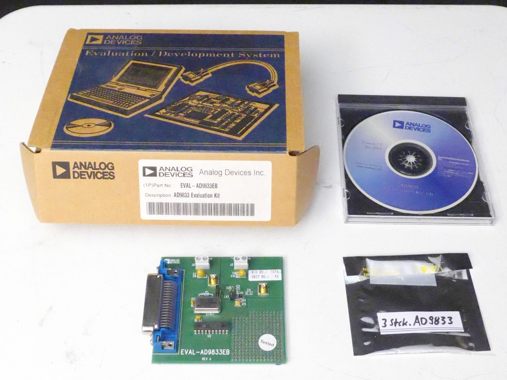
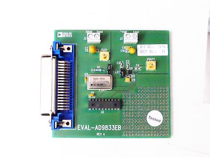
Analog Devices EVAL-AD9833 Evaluation Kit mit CD und Platine
ANALOG DEVICES Evaluation / Development System (1P) Part No EVAL-AD9833EB Description: AD9833 Evaluation Kit Analog Devices Inc. EVAL-AD9833EB REV A 3 stk. AD9833
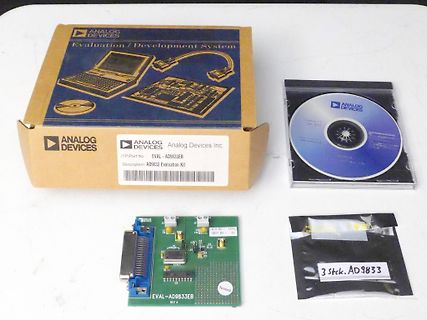
in „[V] AD9833-Eval-Kit; Programmable Waveform-Generator“ · Markt · · Fotos
-
Datei
ad9833_beispiel.asm
.include "m8def.inc" ;Dieses Programm zeigt ein Beispiel mit dem AD9833. ;Es kommuniziert mit dem AD9833 über SPI. ;Mit diesem Programm erzeugt der AD9833 ein Sinussignal ;mit einer Frequenz von 1kHz .org 0x00 rjmp reset .def temp = r16 .def s_data_low = r17 ;Serielle
in „Beispielprogramm AD9833 (DDS) mit atmega8“ · Projekte & Code ·
-
PDF
-
Datei
ad9833.txt
#include <p33FJ128MC706.h> #include <dsp.h> #include <libpic30.h> #include "..\h\manualSPI.h" void SPI3_send(int data) { int i; for(i=0;i<16;i++) { SPI3_OUT =((data >> i) & 0x01); delay_ms(10); SPI3_CLK = 1; delay_ms(10); SPI3_CLK = 0; //data >>= 1; } } void SPI3_start(void) { SPI3_CS = 1; delay_ms(10); SPI3_CLK = 1; delay_ms(10); SPI3_CS = 0; delay_ms(10); } void SPI3_end(void) { //delay_ms(10); SPI3_CS = 1; delay_ms(10); } void init_dds(void) { int data; TRISD = 0; data = 0x2108; // Reset registers SPI3_start(); SPI3_send(data); SPI3_end(); data = 0x75C3; // 14 LSB's of FREQ0 SPI3_start(); SPI3
in „ad9833 codefrage [not working]“ · Mikrocontroller und Digitale Elektronik ·
-
Datei
AD9833.ino
#include "Wire.h" #include "TimerOne.h" int FSYNC = 6; int SDATA = 7; int SCLK = 8; int LED = 3; int Taster = 2; int Start = 0; unsigned long erg; unsigned long freq=0; byte wave=1; char ser='w'; int alle_x_sekunden=1; int aktiv=1; void setup() { pinMode(LED, OUTPUT); pinMode(Taster, INPUT); pinMode(FSYNC, OUTPUT); pinMode(SDATA, OUTPUT); pinMode(SCLK, OUTPUT); digitalWrite(FSYNC, HIGH); digitalWrite(SDATA, LOW); digitalWrite(SCLK, HIGH); Wire.begin(); Serial.begin(38400); UpdateRegister(0x2100); // Nach Application Note AN-1070 von Analog Devices UpdateRegister(0x50C7); UpdateRegister(0x4000)
in „Sweep Generator mit AD5930“ · Mikrocontroller und Digitale Elektronik ·
-
Bild
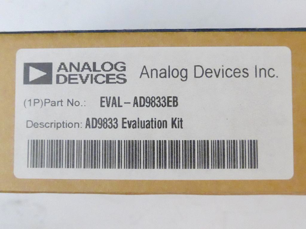
Etikett eines Analog Devices Evaluation Kits
ANALOG DEVICES Analog Devices Inc. (1P)Part No.: EVAL-AD9833EB Description: AD9833 Evaluation Kit
in „[V] AD9833-Eval-Kit; Programmable Waveform-Generator“ · Markt · · Fotos
-
Datei
sweep.ino
// for chip info see https://www.analog.com/en/products/ad9833.html // SPI code taken from https://github.com/MajicDesigns/MD_AD9833/ const uint8_t _dataPin = 7; const uint8_t _clkPin = 8; const uint8_t _fsyncPin = 6; // send raw 16-bit word void spiSend(const
in „Arduino+AD9833 code für Rechteckfestfrequenz“ · Mikrocontroller und Digitale Elektronik ·
-
Bild
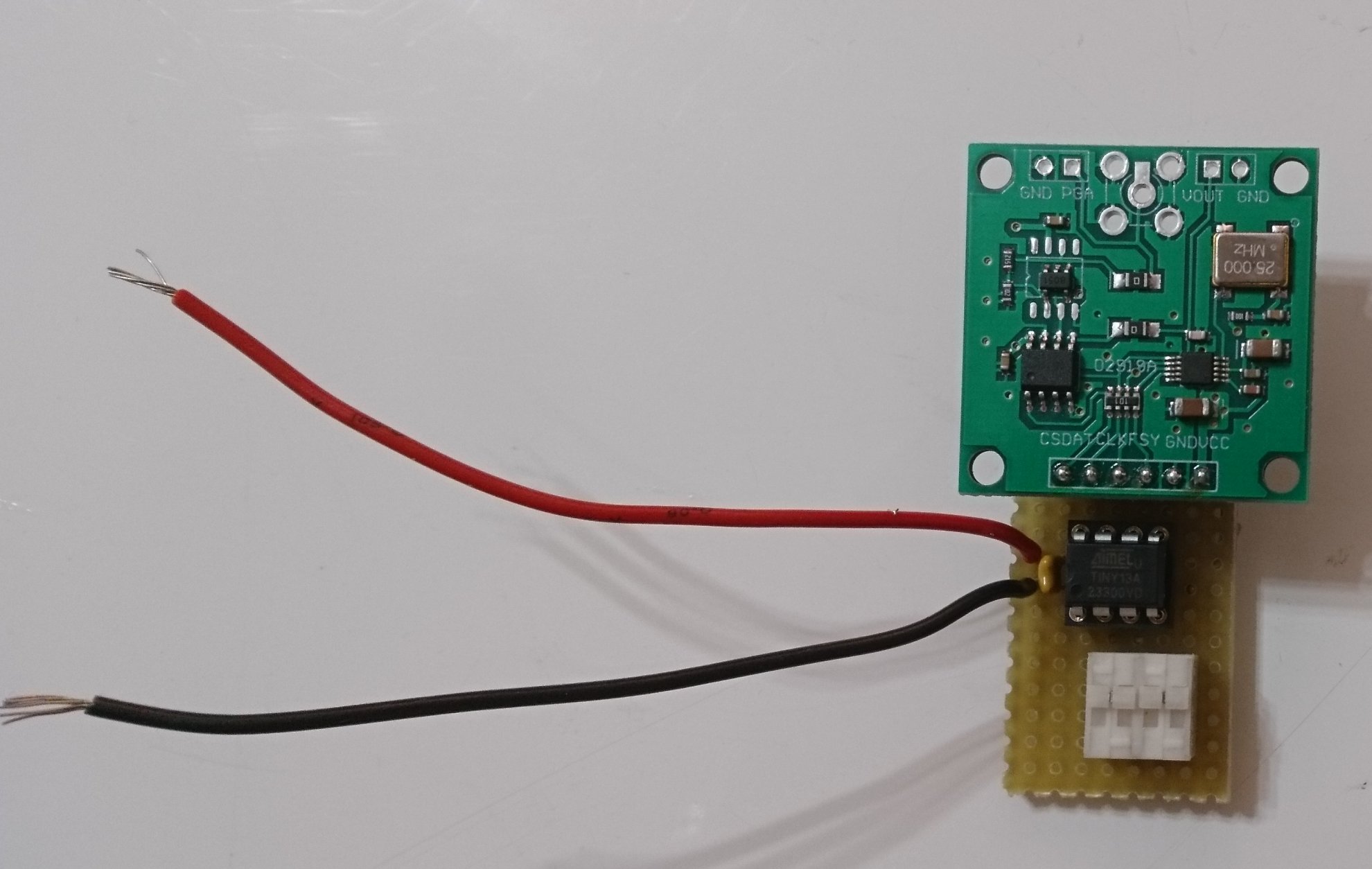
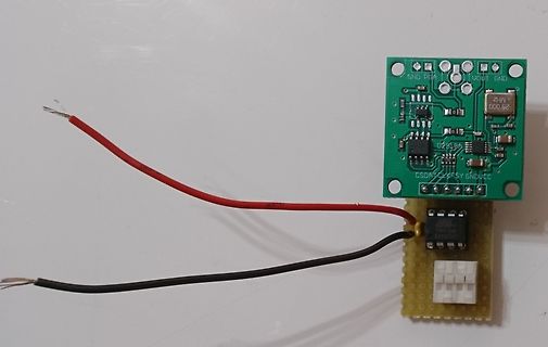
Zwei Leiterplatten mit Kabeln und Bauteilen
GND PGA VOUT GND 25.000 MHZ 029199 CSDA TCK FSY GNDUCC
in „AD9833 Programmieren“ · Mikrocontroller und Digitale Elektronik · · Platinenfotos
-
Bild
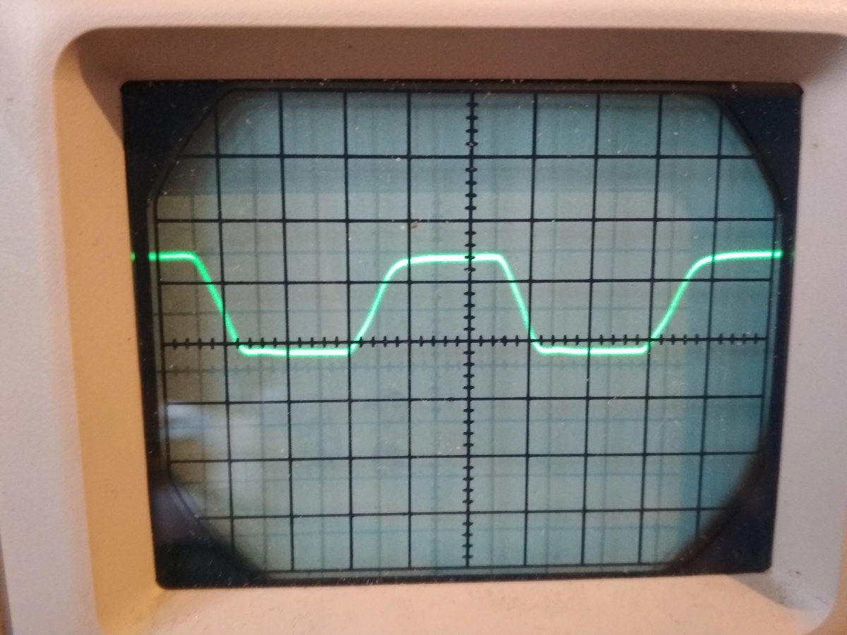
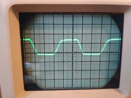
Oszilloskop-Bildschirm mit Rechtecksignal
AD9833__Rechteck.jpg
in „Arduino+AD9833 code für Rechteckfestfrequenz“ · Mikrocontroller und Digitale Elektronik · · Fotos
-
Datei
cfg_ad9833.c
/* * Konfiguration vom AD9833 * */ #include <avr/io.h> #include <avr/sleep.h> // ftw = freq * ACCU_SIZE / F_DDS // = freq * 2^28 / 25e6 Hz // = freq * 10.73741824 // Manuelle Berechnung fuer 5845000 Hz // FTW frequency tuning word
in „AD9833 Programmieren“ · Mikrocontroller und Digitale Elektronik ·
-
Bild
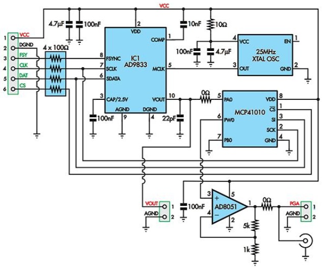
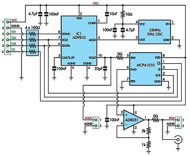
Schaltplan einer analogen Schaltung mit AD9833 und MCP41010
VCC, 4.7µF, 100nF, IC1 AD9833, 10Ω, 25MHz XTAL OSC, EN, VDD, COMP, FSYNC, CLK, SCLK, SDATA, CS, CAP/2.5V, MCLK, OUT, GND, 100nF, 4.7µF, 0Ω, MCP41010, VOUT, DGND, PA0, CS, 3, SI, SCK, PBO, 22pF, GND, 100nF, AD8051, VOUT, AGND, PGA
in „AD9833 Modul mit MCP41010“ · Mikrocontroller und Digitale Elektronik · · Schaltpläne
-
Bild
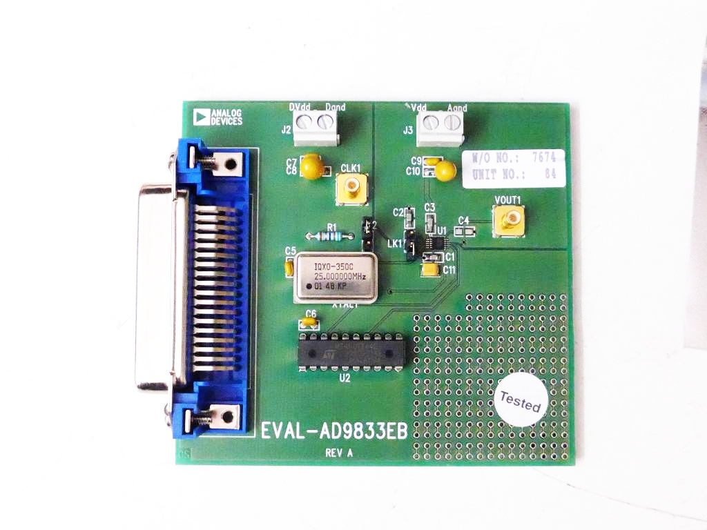
Analog Devices EVAL-AD9833EB Evaluation Board
C8 CLK1 C9 C10 C2 C3 C4 VOUT1 LK1 U1 C1 C11 C5 IQXO-350C 25.000000MHZ 01 48 KP C6 U2 Tested EVAL-AD9833EB REV A
in „[V] AD9833-Eval-Kit; Programmable Waveform-Generator“ · Markt · · Platinenfotos