-
 Bild
Bild
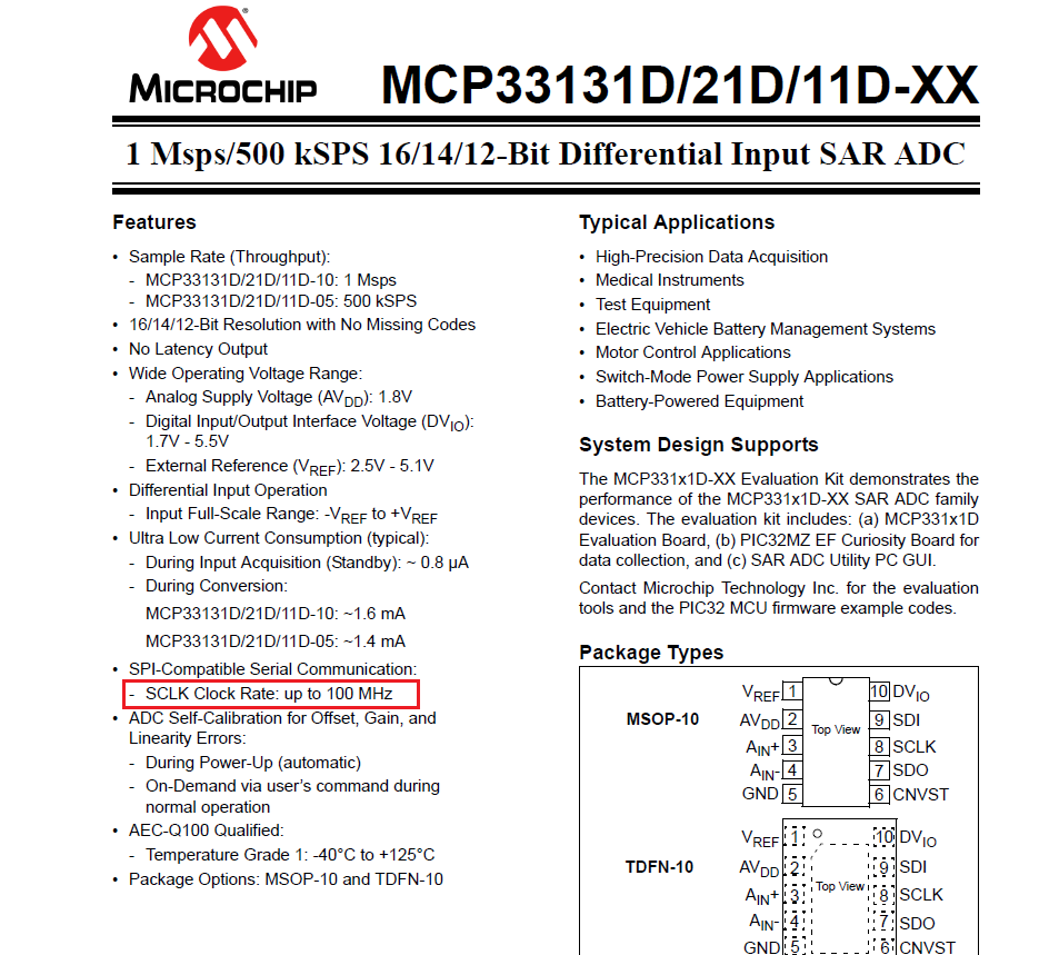
Datenblatt Ausschnitt MCP33131D SAR ADC
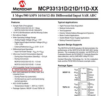
MICROCHIP MCP33131D/21D/11D-XX 1 Msps/500 kSPS 16/14/12-Bit Differential Input SAR ADC Features Sample Rate (Throughput) MCP33131D/21D/11D-10: 1 Msps MCP33131D/21D/11D-05: 500 kSPS 16/14/12-Bit Resolution with No
-
 Bild
Bild
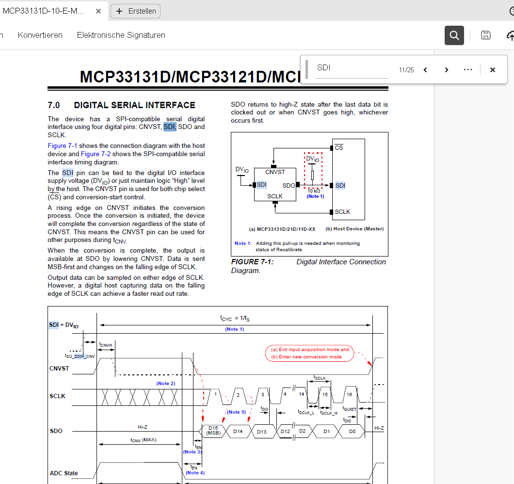
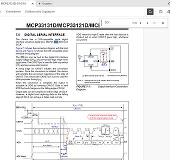
Datenblatt Ausschnitt MCP33131D Digital Interface
MCP33131D/MCP33121D/MCI 7.0 DIGITAL SERIAL INTERFACE SDI, SDO, SCLK, CNVST FIGURE 7-1: Digital Interface Connection Diagram. (a) MCP33131D/21D/11D-XX (b) Host Device (Master) SDI = DVIO tCYC = 1/fs CNVST
-
 Bild
Bild
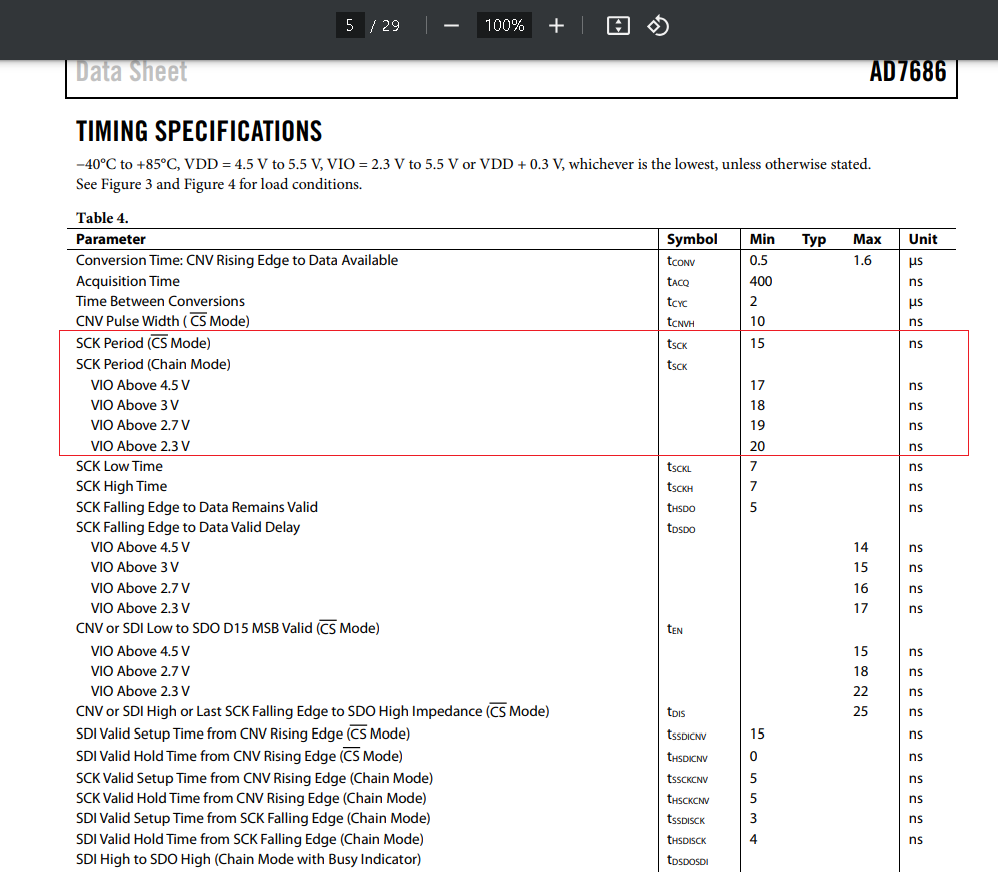
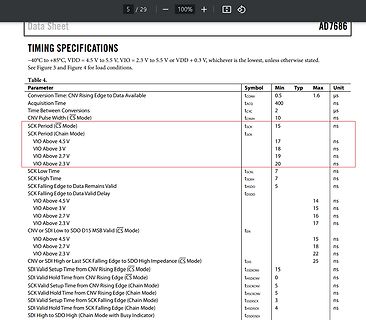
Datenblatt Timing Spezifikationen AD7686
Data Sheet AD7686 TIMING SPECIFICATIONS -40°C to +85°C, VDD = 4.5 V to 5.5 V, VIO = 2.3 V to 5.5 V or VDD + 0.3 V, whichever is the lowest, unless otherwise stated. See Figure 3 and Figure 4 for load conditions. Table 4. Parameter Symbol Min Typ Max Unit Conversion Time CNV Rising Edge to Data Available tCONV 0.5 1.6 µs Acquisition Time tACQ 400 ns Time Between Conversions tCYC 2 µs CNV Pulse Width (CS Mode) tCNVH 10 ns SCK Period (CS Mode) tSCK 15 ns VIO Above 4.5 V 17 ns VIO Above 3 V 18 ns VIO Above 2.7 V 19 ns VIO Above 2.3 V 20 ns SCK Low Time tSCKL 7 ns SCK High Time tSCKH 7 ns SCK Falling Edge
-
 Bild
Bild
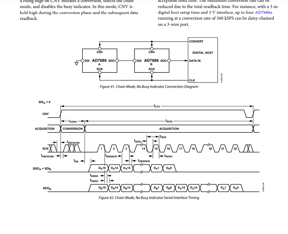
Datenblatt Blockschaltbild und Timing-Diagramm AD7686
a rising edge on CNV initiates a conversion, selects the chain mode, and disables the busy indicator. In this mode, CNV is held high during the conversion phase and the subsequent data readback. AD7686 CONVERT DIGITAL HOST DATA IN CLK Figure 41. Chain Mode, No Busy Indicator Connection Diagram SDI_A = 0 CNV ACQUISITION CONVERSION SCK SDO_A = SDO_B SDO_B Figure 42. Chain Mode, No Busy Indicator Serial Interface Timing