-
 Bild
Bild
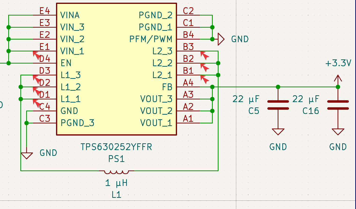
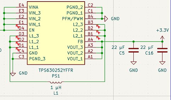
Schaltplan eines TPS630252YFFR Spannungswandlers
1 A4 D1 L1_1 FB A3 C4 GND A3 VOUT_3 A2 C3 PGND_3 VOUT_2 A1 VOUT_1 +3.3V 22 uF C5 22 uF C16 GND GND TPS630252YFFR PS1 1 uH L1 GND
-
 Bild
Bild
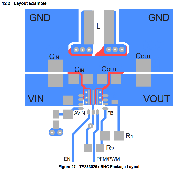
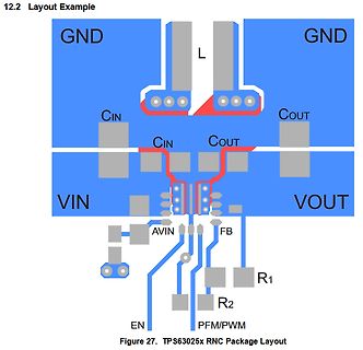
PCB-Layout Beispiel für TPS63025x RNC Package
12.2 Layout Example GND L GND CIN COUT CIN COUT VIN VOUT AVIN FB R1 R2 EN PFM/PWM Figure 27. TPS63025x RNC Package Layout
-
 Bild
Bild
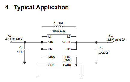
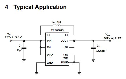
Schaltplan eines TPS63025 Step-Down-Wandlers
4 Typical Application L1 1uH TPS63025 VIN L1 L2 VOUT VIN 2.7 V to 5.5 V C1 10uF EN FB VINA PFM/PWM PFM/PWM GND PGND Vin out 3.3 V up to 2A C2 2X22uF
-
 Bild
Bild
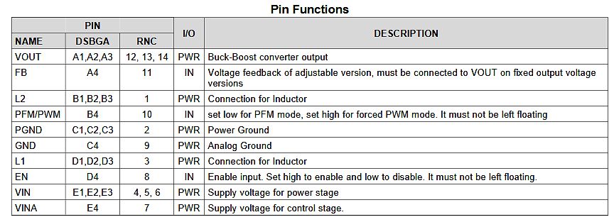
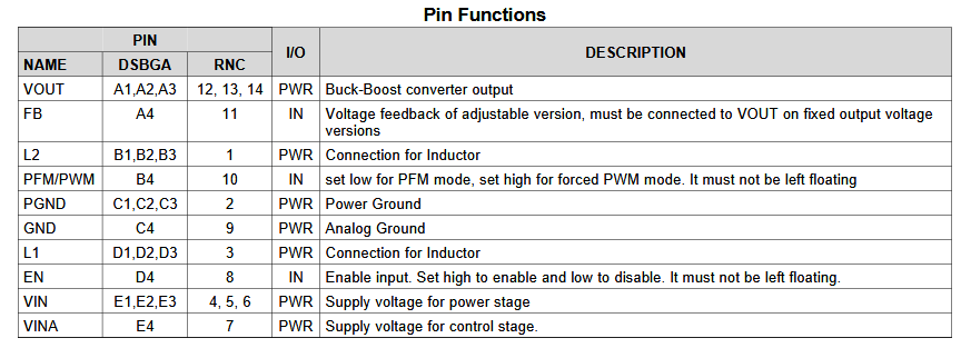
Pin-Funktionstabelle eines ICs
Pin Functions NAME DSBGA RNC I/O DESCRIPTION VOUT A1,A2,A3 12, 13, 14 PWR Buck-Boost converter output FB A4 11 IN Voltage feedback of adjustable version, must be connected to VOUT on fixed output voltage versions L2 B1,B2,B3 1 PWR Connection for Inductor PFM/PWM B4 10 IN set low for PFM mode, set high for forced PWM mode. It must not be left floating PGND C1,C2,C3 2 PWR Power Ground GND C4 9 PWR Analog Ground L1 D1,D2,D3 3 PWR Connection for Inductor EN D4 8 IN Enable input. Set high to enable and low to disable. It must not be left floating. VIN E1,E2,E3 4, 5, 6 PWR Supply voltage for power stage