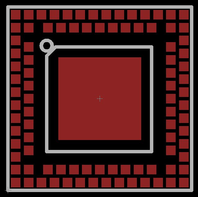
Hi,

ich mache gerade das Footprint des Silabs SIM3U167-B-GM im LGA92 Package
(siehe Bild) in Eagle.
Das ist mein erstes Footprint von einem LGA.
Im Datasheet

http://www.silabs.com/pages/DownloadDoc.aspx?FILEURL=Support%20Documents/TechnicalDocs/SiM3U1xx.pdf&src=DocumentationWebPart

Seite 76, steht geschrieben:

6.1.1. LGA-92 Solder Mask Design
All metal pads are to be non-solder mask defined (NSMD). Clearance
between the solder mask and the metal pad is to be 60 μm minimum, all
the way around the pad.
6.1.2. LGA-92 Stencil Design
1. A stainless steel, laser-cut and electro-polished stencil with
trapezoidal walls should be used to assure
good solder paste release.
2. The stencil thickness should be 0.125 mm (5 mils).
3. The ratio of stencil aperture to land pad size should be 1:1 for all
perimeter pins.
4. A 2 x 2 array of 1.25 mm square openings on 1.60 mm pitch should be
used for the center ground pad.
6.1.3. LGA-92 Card Assembly
1. A No-Clean, Type-3 solder paste is recommended.
2. The recommended card reflow profile is per the JEDEC/IPC J-STD-020
specification for Small Body
Components.


Wie kann ich eine Clearance Fläche :"Clearance between the *solder mask
and the metal pad is to be 60 μm minimum*, all the way around the pad."

60µ um die Pads herum machen? Ich finde auch die Layer Clearance nicht
in Eagle.


Habt ihr einen Tipp?

Viele Grüße
Harald
Angehängte Dateien:
-
 LGA92.JPG
(53 KB)
LGA92.JPG
(53 KB)