1 |
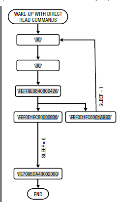
int8_t LTC2949_Wakeup_isoSpi (LTC2949_t *dev)
|
2 |
{
|
3 |
uint8_t data = 0x00;
|
4 |
|
5 |
HAL_GPIO_WritePin(dev->cs_port, dev->cs_pin, GPIO_PIN_RESET);
|
6 |
HAL_SPI_Transmit(dev->spi, &data, 1, 1);
|
7 |
HAL_GPIO_WritePin(dev->cs_port, dev->cs_pin, GPIO_PIN_SET);
|
8 |
|
9 |
return 0;
|
10 |
}
|
11 |
|
12 |
|
13 |
int8_t LTC2949_Read_Reg (LTC2949_t *dev, uint8_t *data, uint8_t address, uint8_t length)
|
14 |
{
|
15 |
// Compute the frame length and PECC
|
16 |
uint8_t frame_length = 5 + length + 2;
|
17 |
uint8_t pecc = length - 1;
|
18 |
|
19 |
// Set pointers to various parts of the buffers
|
20 |
uint8_t *tx_data_1 = dev->tx_buff;
|
21 |
uint8_t *rx_data = dev->rx_buff + 5;
|
22 |
uint16_t *tx_pec_1 = (uint16_t*) (dev->tx_buff + 2);
|
23 |
uint16_t *rx_pec = (uint16_t*) (dev->rx_buff + 5 + length);
|
24 |
|
25 |
// Variables for storing the received PEC and checking for errors
|
26 |
uint16_t rx_pec_calc;
|
27 |
uint8_t rx_pec_error = 0;
|
28 |
|
29 |
// Configure the MOSI frame
|
30 |
tx_data_1[0] = 0xFE; // Direct Read/Write Command
|
31 |
tx_data_1[1] = address;
|
32 |
*tx_pec_1 = swap_bytes(pec15(tx_data_1, 2));
|
33 |
|
34 |
tx_data_1[4] = (1 << 7) + (0 << 6); // read command
|
35 |
tx_data_1[4] += (((pecc >> 3) & 0x1) ^ ((pecc >> 2) & 0x1)) << 5;
|
36 |
tx_data_1[4] += ((pecc >> 3) & 0x1) << 4;
|
37 |
tx_data_1[4] += ((pecc >> 2) & 0x1) << 3;
|
38 |
tx_data_1[4] += (((pecc >> 1) & 0x1) ^ ((pecc >> 0) & 0x1)) << 2;
|
39 |
tx_data_1[4] += ((pecc >> 1) & 0x1) << 1;
|
40 |
tx_data_1[4] += ((pecc >> 0) & 0x1) << 0;
|
41 |
|
42 |
|
43 |
// Transmit and receive the data using DMA
|
44 |
HAL_GPIO_WritePin(dev->cs_port, dev->cs_pin, GPIO_PIN_RESET);
|
45 |
HAL_SPI_TransmitReceive_DMA(dev->spi, dev->tx_buff, dev->rx_buff, frame_length);
|
46 |
|
47 |
// Wait for the DMA transfer to complete
|
48 |
while(dev->spi->hdmatx->State != HAL_DMA_STATE_READY || dev->spi->hdmarx->State
|
49 |
!= HAL_DMA_STATE_READY);
|
50 |
|
51 |
// Release the CS pin
|
52 |
HAL_GPIO_WritePin(dev->cs_port, dev->cs_pin, GPIO_PIN_SET);
|
53 |
|
54 |
// Copy the received data to the output buffer
|
55 |
memcpy(data, rx_data, length);
|
56 |
|
57 |
// Compute RX PEC to compare it with the transmitted
|
58 |
rx_pec_calc = swap_bytes(pec15(rx_data, length));
|
59 |
if(*rx_pec != rx_pec_calc) rx_pec_error = 1;
|
60 |
|
61 |
|
62 |
// Return error code if PEC error occurred, otherwise return success
|
63 |
if(rx_pec_error)
|
64 |
return -1;
|
65 |
else
|
66 |
return 0;
|
67 |
}
|
68 |
|
69 |
int8_t LTC2949_Write_Reg (LTC2949_t *dev, uint8_t *data, uint8_t address, uint8_t length)
|
70 |
{
|
71 |
// Compute the frame length and PECC
|
72 |
uint8_t frame_length = 5 + length + 2;
|
73 |
uint8_t pecc = length - 1;
|
74 |
|
75 |
// Set pointers to various parts of the buffers
|
76 |
uint8_t *tx_data_1 = dev->tx_buff;
|
77 |
uint8_t *tx_data_2 = dev->tx_buff + 5;
|
78 |
uint8_t *rx_data = dev->rx_buff + 5;
|
79 |
uint16_t *tx_pec_1 = (uint16_t*) (dev->tx_buff + 2);
|
80 |
uint16_t *tx_pec_2 = (uint16_t*) (dev->tx_buff + 5 + length);
|
81 |
uint16_t *rx_pec = (uint16_t*) (dev->rx_buff + 5 + length);
|
82 |
|
83 |
// Variables for storing the received PEC and checking for errors
|
84 |
uint16_t rx_pec_calc;
|
85 |
uint8_t rx_pec_error = 0;
|
86 |
|
87 |
// Configure the MOSI frame
|
88 |
tx_data_1[0] = 0xFE; // Direct Read/Write Command
|
89 |
tx_data_1[1] = address;
|
90 |
*tx_pec_1 = swap_bytes(pec15(tx_data_1, 2));
|
91 |
|
92 |
tx_data_1[4] = (0 << 7) + (1 << 6); // write command
|
93 |
tx_data_1[4] += (((pecc >> 3) & 0x1) ^ ((pecc >> 2) & 0x1)) << 5;
|
94 |
tx_data_1[4] += ((pecc >> 3) & 0x1) << 4;
|
95 |
tx_data_1[4] += ((pecc >> 2) & 0x1) << 3;
|
96 |
tx_data_1[4] += (((pecc >> 1) & 0x1) ^ ((pecc >> 0) & 0x1)) << 2;
|
97 |
tx_data_1[4] += ((pecc >> 1) & 0x1) << 1;
|
98 |
tx_data_1[4] += ((pecc >> 0) & 0x1) << 0;
|
99 |
|
100 |
// Copy the data to the transmit buffer
|
101 |
memcpy(tx_data_2, data, length);
|
102 |
|
103 |
// Compute the PEC for the second part of the transmit buffer
|
104 |
*tx_pec_2 = swap_bytes(pec15(tx_data_2, length));
|
105 |
|
106 |
// Transmit and receive the data using DMA
|
107 |
HAL_GPIO_WritePin(dev->cs_port, dev->cs_pin, GPIO_PIN_RESET);
|
108 |
HAL_SPI_TransmitReceive_DMA(dev->spi, dev->tx_buff, dev->rx_buff, frame_length);
|
109 |
|
110 |
// Wait for the DMA transfer to complete
|
111 |
while(dev->spi->hdmatx->State != HAL_DMA_STATE_READY || dev->spi->hdmarx->State
|
112 |
!= HAL_DMA_STATE_READY);
|
113 |
|
114 |
// Release the CS pin
|
115 |
HAL_GPIO_WritePin(dev->cs_port, dev->cs_pin, GPIO_PIN_SET);
|
116 |
|
117 |
// Compute RX PEC to compare it with the transmitted
|
118 |
rx_pec_calc = swap_bytes(pec15(rx_data, length));
|
119 |
if(*rx_pec != rx_pec_calc) rx_pec_error = 1;
|
120 |
|
121 |
|
122 |
// Return error code if PEC error occurred, otherwise return success
|
123 |
if(rx_pec_error)
|
124 |
return -1;
|
125 |
else
|
126 |
return 0;
|
127 |
}
|
128 |
|
129 |
|
130 |
int8_t LTC2949_Init (LTC2949_t *dev, SPI_HandleTypeDef *spi, GPIO_TypeDef *cs_port,
|
131 |
uint16_t cs_pin)
|
132 |
{
|
133 |
// Store parameters in device struct
|
134 |
dev->spi = spi;
|
135 |
dev->cs_port = cs_port;
|
136 |
dev->cs_pin = cs_pin;
|
137 |
dev->address = 0x0F; // Constant for every LTC2949
|
138 |
|
139 |
// Initialize PEC15 table
|
140 |
init_PEC15_Table();
|
141 |
|
142 |
// Set CS pin high, low, high to wake up LTC249 core
|
143 |
HAL_GPIO_WritePin(dev->cs_port, dev->cs_pin, GPIO_PIN_SET);
|
144 |
HAL_GPIO_WritePin(dev->cs_port, dev->cs_pin, GPIO_PIN_RESET);
|
145 |
HAL_GPIO_WritePin(dev->cs_port, dev->cs_pin, GPIO_PIN_SET);
|
146 |
|
147 |
uint32_t start = HAL_GetTick();
|
148 |
while(1)
|
149 |
{
|
150 |
// Check if initialization has taken longer than 120ms
|
151 |
if(start + 120 <= HAL_GetTick()) return -1;
|
152 |
|
153 |
uint8_t data = 0x00;
|
154 |
|
155 |
// Wake up the LTC2949 twice to ensure it's responsive
|
156 |
LTC2949_Wakeup_isoSpi(dev);
|
157 |
LTC2949_Wakeup_isoSpi(dev);
|
158 |
|
159 |
// Set page 0 and direct read mode in REGSCTRL register
|
160 |
data = 0 + (1 << 7);
|
161 |
LTC2949_Write_Reg(dev, &data, 0xFF, 1);
|
162 |
|
163 |
// Read OPCTRL register to check if the LTC2949 core is in sleep mode
|
164 |
LTC2949_Read_Reg(dev, &data, 0xF0, 1);
|
165 |
|
166 |
// Continue looping if sleeping
|
167 |
if((data & 0x01) != 0) continue;
|
168 |
|
169 |
// Disable sleep mode
|
170 |
data = 0x00;
|
171 |
LTC2949_Write_Reg(dev, &data, 0x70, 1);
|
172 |
break;
|
173 |
}
|
174 |
return 0;
|
175 |
}
|

 Frame.PNG
(14 KB)
Frame.PNG
(14 KB)
 Schaltplan.png
(43 KB)
Schaltplan.png
(43 KB)
 Vip_-_Vim.png
(29 KB)
Vip_-_Vim.png
(29 KB)