-
Thread
DigiTrainer – browserbasierter Simulator des ITT Digi-Trainer 2 (Open Source)
Als nächste Erweiterungen sind unter anderem eine visuelle Anzeige der Schiebeschalter und der der HIGH/LOW-Pegel an den Steckbuchsen, das Speichern und Laden von Schaltungen sowie möglicherweise ein virtueller Signalprüfer vorgesehen. Mich würden besonders eure Meinungen zur technischen Umsetzung
-
 Bild
Bild
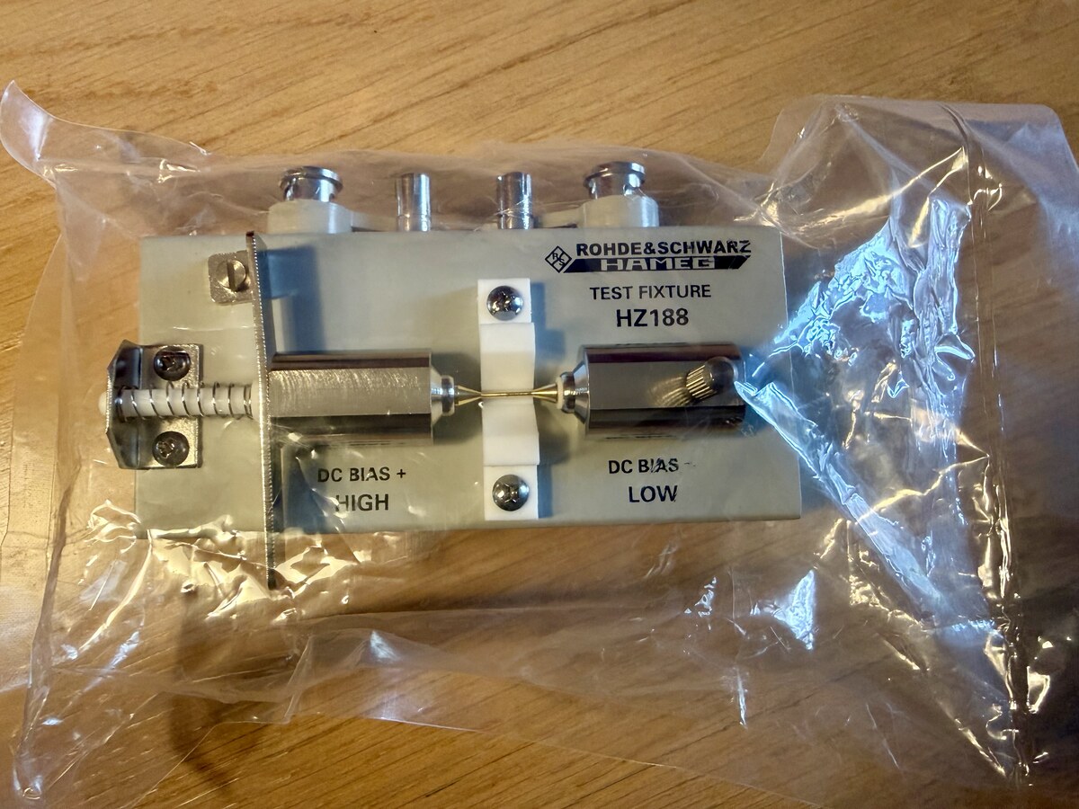
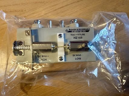
Rohde & Schwarz Hameg Test Fixture HZ188
ROHDE & SCHWARZ HAMEG TEST FIXTURE HZ188 DC BIAS + HIGH DC BIAS - LOW
-
 Bild
Bild
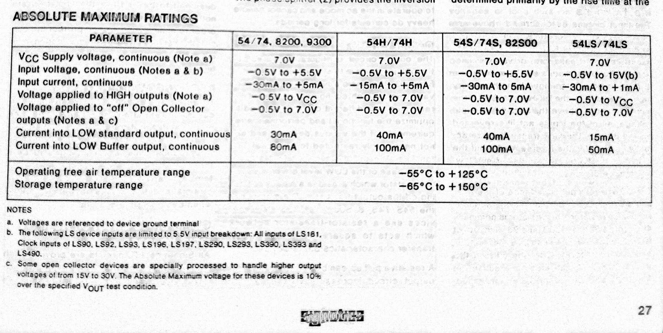
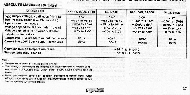
Tabelle der absoluten Maximalwerte eines Datenblatts
Input current, continuous -30mA to +5mA -15mA to +5mA -30mA to 5mA -30mA to +1mA Voltage applied to HIGH outputs (Note a) -0.5V to VCC -0.5V to 7.0V -0.5V to 7.0V -0.5V to VCC Voltage applied to "off" Open Collector outputs (Notes a & c) -0.5V to 7.0V -0.5V to 7.0V -0.5V to 7.0V -0.5V to 7.0V Current into LOW standard output, continuous 30mA 40mA 40mA 15mA Current into LOW Buffer, continuous 80mA 100mA 100mA 50mA Operating free air temperature range -55°C to +125°C Storage temperature range -65°C to +150
-
Thread
Espressif startet Verkauf von Mosaico, Arduino professionalisiert App Lab, Weltraumelektronik uvam
store.mosaico.ai/products/esp-mosaico ### LILYGO T-Halow P4 – ESP32-P4 mit M.2-2280-Interface und WiFi HaLow Das M.2-Interface hat sich im Bereich der Einplatinencomputer mittlerweile als Quasi-Standard etabliert. Nun gibt es im Hause LILYGO eine Entwicklungsplatine, die – wie in der Abbildung gezeigt – über
bekannte Kombination aus ESP32-P4 und ESP32-C6. Hervorzuheben ist, dass außerdem auch ein Wi-Fi-HaLow-Modul auf der Platine verbaut ist. Wer das Produkt käuflich erwerben möchte, kann dies unter anderem auf AliExpress tun. 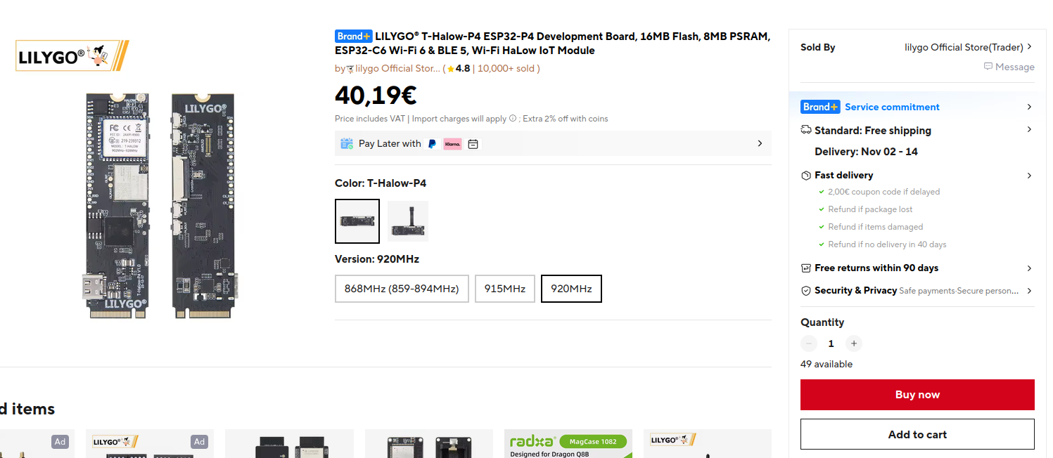 Bildquelle: https://s.click.aliexpress.com
-
 Bild
Bild
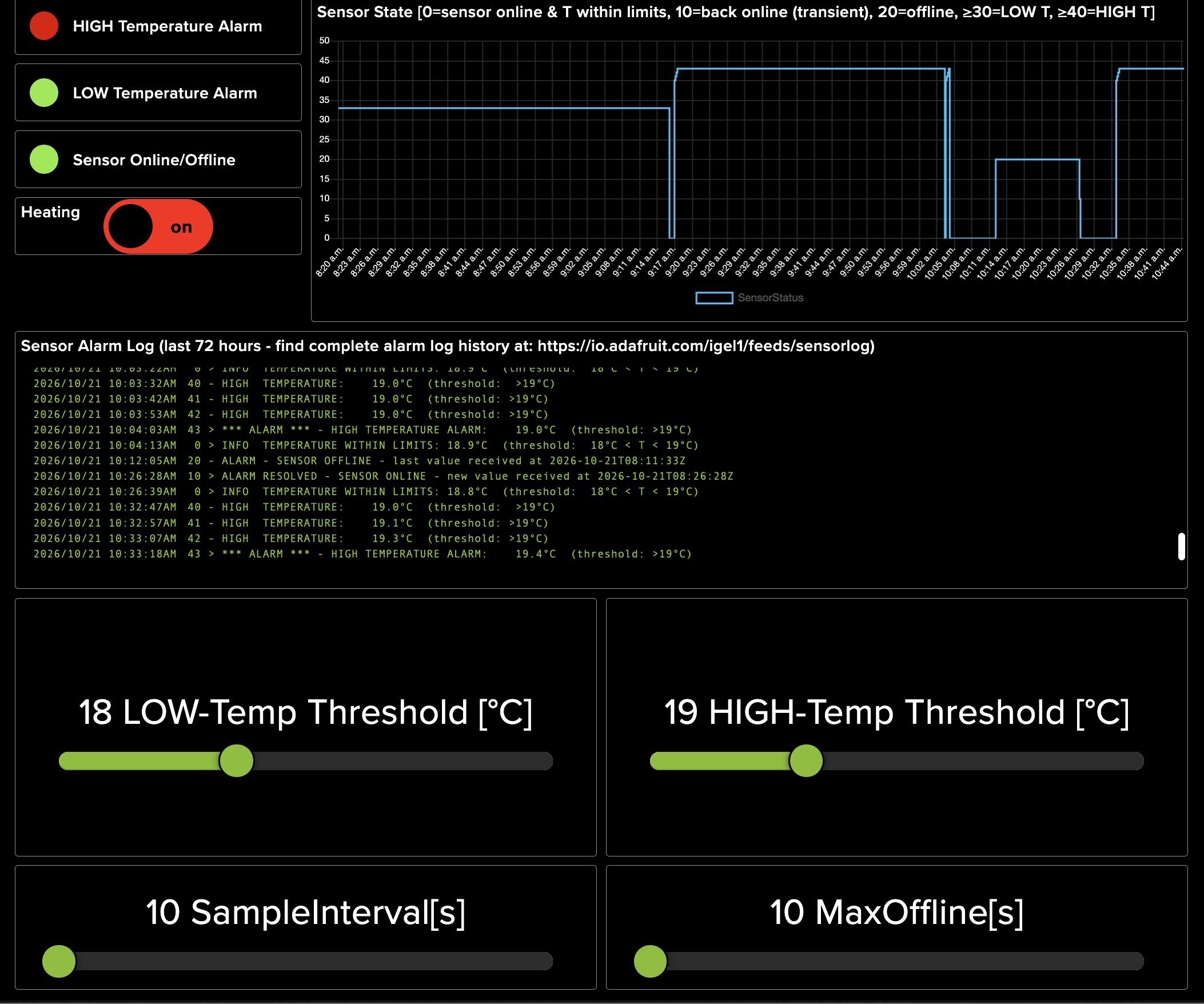
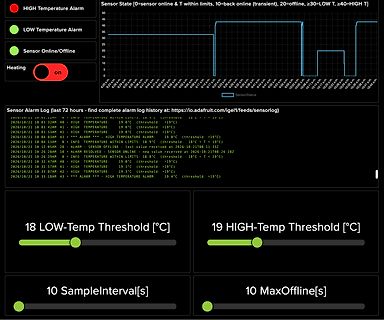
Dashboard einer Temperaturüberwachung mit Graph und Log
HIGH Temperature Alarm LOW Temperature Alarm Sensor Online/Offline Heating on Sensor State [0=sensor online & T within limits, 10=back online (transient), 20=offline, >=30=LOW T, >=40=HIGH T] SensorStatus
-
 Bild
Bild
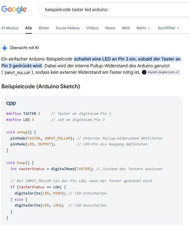
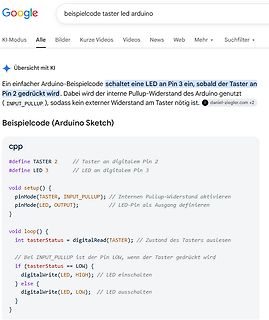
Google-Suchergebnisse für Arduino-Beispielcode
tasterStatus = digitalRead(TASTER); // Zustand des Tasters auslesen // Bei INPUT_PULLUP ist der Pin LOW, wenn der Taster gedrückt wird if (tasterStatus == LOW) { digitalWrite(LED, HIGH); // LED einschalten } else { digitalWrite(LED, LOW); // LED ausschalten }
-
Thread
KiCAD: Erste Gehversuche - bitte um Feedback
Mein Freund soll per Email alarmiert werden, wenn von ihm konfigurierbare Temperaturschwellen (LOW/HIGH) unter-/überschritten werden. - Mein Freund soll informiert werden, wenn sein Sensor keine Daten mehr in die Cloud schickt. - Mein Freund soll mit einem Blick auf die 3 Indikatoren auf
berechnet werden. Und weil so viele fragen, wie man mit einem Heizwiderstand "kühlen" kann, um die LOW-Temperatur-Alarmierung zu testen: - Hier in meinem Zimer sind es aktuell 20 Grad - Also stelle ich die LOW-Schwelle auf 21 Grad und die HIGH-Schwelle auf 22 Grad - Dann Heizwiderstand an -> der