-
Bild
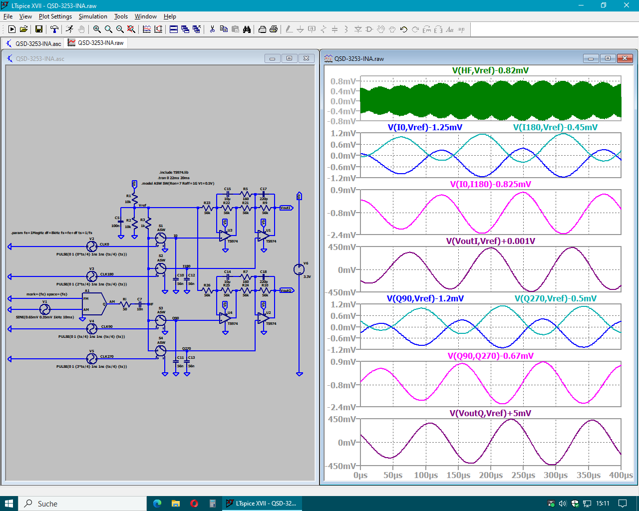
LTspice Simulation Schaltplan und Wellenformen
LTspice XVII QSD-3253-INA.raw File View Plot Settings Simulation Tools Window Help QSD-3253-INA.asc QSD-3253-INA.raw C1 C10 C11 C12 C13 R22 R23 R25 R26 R27 R28 R29 R30 R31 R32 R33 R34 R35 R36 R37 R38 R39 R40 R41 R42 R43 R44
in „Raspberry Pi Pico SDR“ · HF, Funk und Felder · · Screenshots
-
PDF
Orion_Rev_3.0__1_.pdf
DB6 51 1 6 9 1 V- 9 DA7 28 INA7 V- 12 12 DB7 52 20 V- 17 ENC DA8 29 INA8 C J31 C76 C75 GND V- R45 DB8 53 C 3 DA9 INA9 100NF 100PF 51 DB9 30 1 LTC6400-20 R44 DA10 54 INA10 DB10 33 2 55 INA11 51 13 DA11 34 RX1 IN MICRO COAXIAL L11
in „Suche Firma die für Privat BGA FPGA reballing macht“ · Markt ·
-
PDF
rudi_____RX-V4A_TSR-400.pdf
T32A05INB1/T32A05INC0/T32A05INA0/ 143 USB_VBUS_PRT +3.3S_PON I I USB Power Feedback AINA10/PP2 144 T32A05INA1/T32A05INC1/T32A05INB0/ TEST1 +3.3S_PON I I AINA11/PP3 145 T32A06INB1/T32A06INC0/T32A06INA0/ MODE +3.3S_PON I I AINA12/PP4 T32A06INA1/T32A06INC1/T32A06INB0/ 146 AINA13/PP5 TEST2 +3.3S_PON I I T32A07INB1/T32A07INC0/T32A07INA0/ 147 STBY_LED AC O O Standby LED control INT10b/AINA14/PP6 148 T32A07INA1/T32A07INC1/T32A07INB0/ DSP2_NIC
in „Test in der Schaltung STR3A400“ · Analoge Elektronik und Schaltungstechnik ·
-
PDF
tps63020.pdf
IN= VINA= 3.6 V, A = 25°C 3500 4000 4500 mA High side switch on resistance V = V = 3.6 V 50 mΩ IN INA Low side switch on resistance V IN= VINA= 3.6 V 50 mΩ Quiescent VIN and VINA IOUT = 0 mA, VEN= V IN= VINA= 3.6 25 50 μA q current V, VOUT V OUT = 3.3 V 5 10 μA TPS63021 FB input impedance V EN = HIGH 1 MΩ I Shutdown current V = 0 V, V = V = 3.6 V 0.1 1 μA S EN IN INA CONTROL STAGE Under voltage lockout threshold V INAvoltage decreasing 1.4 1.5 1.6 V UVLO Under voltage lockout hysteresis 200 mV VIL EN, PS/SYNC input low voltage 0.4 V VIH EN, PS/SYNC input high voltage
in „ESP32-H2 will nicht schlafen“ · Mikrocontroller und Digitale Elektronik ·
-
PDF
pm2521ocr.pdf
by the voltagedivisionoftheseriescomponents R101//C101, C102 and the sC100.omponents R101, R103, R106//C103, C“04, C10sblocked byco:ponent atthe inputi — x20 attenuation isprovided by R101//C106, C10,, C108 switched by relay K101; — x200 attenuationby R101//C109,C110,C111, C112,C113,switched .y relayK102
in „Pjilips PM2519“ · Markt ·
-
PDF
siplace-s27hm.pdf
deflection unit. . . . . . . . . . . . . . . . . . . . . . . . . . . . . . . . . . . . . . . . . . . 106 4.6.5 Settings . . . . . . . . . . . . . . . . . . . . . . . . . . . . . . . . . . . . . . . . . . . . . . . . . . . . . . . . . . 108 3 Service Manual S-27 HM 10/2005 US Issue 4.7 Replacing the X-axis
in „Siplace 80 Potentialverteiler“ · Mikrocontroller und Digitale Elektronik ·