RatedvoltagerangeU 16…450V a • RoHS compliant n SurgevoltageU U ≤315V:U =1,15U ;U >315V:U =1,10U c S R S R R S R n Max.reversevoltage 2V • REACH compliant t m o Categorytemperaturerange -40°C...+85°C i n LeakagecurrentI afLer5min@U R ≤0,008*C [µFR*U [V]+6RA[µA] , c Usefullife3000h @85°C;U ;I R R Requirements o ΔC/C≤
RatedvoltagerangeU 16…450V a • RoHS compliant n SurgevoltageU U ≤315V:U =1,15U ;U >315V:U =1,10U c S R S R R S R n Max.reversevoltage 2V • REACH compliant t m o Categorytemperaturerange -40°C...+85°C i n LeakagecurrentI afLer5min@U R ≤0,008*C [µFR*U [V]+6RA[µA] , c Usefullife3000h @85°C;U ;I R R Requirements o ΔC/C≤
entlocken. Die Antenne ist die mitgelieferte 30cm-Teleskopantenne. Der NBFM-Receiver ist auf Tau:75u, max Deviation: 5k Was mache ich falsch, oder übersehe ich etwas?
Beitrag #3319831: > Oberhalb 20 MHz hatte ich bisher ohnehin kein verwertbares Signal. Ich melde mal max DX (für 10M) mit einem Silly an. PT9ZE (Brazil) Antenne FB23, Empfänger Silly_Up, FC0013 Stick, SDR# Software
nicht so weit > gekommen. Waren hald nur paar Standpunkte, was hald so gieng. 1,6 Km > länge (max). Naja es hat bloß einfach keinen interessiert. Oder wurde > belächelt. Wurde als "sinnloß" abgestempelt. Was weiß ich. Nächste Woche > trag ich den ganzen Kram zum Recyklinghof. > Servus
Allein schon mit der Erwähnung der Bandbreite. Die BB einer Aussendung darf in diesen Bereichen max. 2,7 KHz betragen (Amateurfunkordnung). Die beschriebenen Sender arbeiteten übrigens im KHz- Bereich (max. im MW- Bereich). Diese Senderart wurde in den 20er Jahren verboten. Und so eine Steinzeit
Max M. schrieb im Beitrag #7292917: > Das ist eine Lehr-CPU. > Anhand der kann man lernen wie man ein Projekt nicht machen sollte, Auch Anti-Patterns sind wichtig! Kein Witz!
Max M. schrieb im Beitrag #7297839: > Josef G. schrieb im Beitrag #7297134: >> https://sedimal.eu > > 'Wir sind für die Einführung des Sedimalsystems Hab ich geändert.
Baßßs Schaßtßeistung des Warnkontaktes: Switching capacit7 oB warning contact: max3 z W induktionsBrei z W max3 noninductiOe etriebstemperatur: ° 2z+C bis 1 A55+C (bis 1 A25+Crating temperature: ° 2z+C to 1 A55+C (up to 1 A25+C max3 A Std3 am 8nschßussgewinde) Bor A hour max3 at threaded
Electrical Characteristics Ta= 25¥;unless otherwise specified. Symbol Parameter Test Condition Min. Typ. Max. Unit System parameters test circuit figure4 VFB Feedback Vin = 3.6V to 10V, Vout=12V 1.213 1.25 1.287 V Voltage Iload=0.1Ato 0.5A Vin=12V ,Vout=18V Efficiency ŋ - 92 - % Iout=3A Electrical Characteristics
handling capability of a transformer is closely dependent on the behaviour of R p as a function of max. For the section of the B-H curve with which we are dealing, B can be calculated using the formula: max B = V /ω × A × n max max in which: B max = maximum flux density in T (2) ω = 2π times frequency
jede Schützenhilfe dankbar. Gruss Juppo #include <stdio.h> #include <stdlib.h> #include "lpc213x.h" //#include <AsystTrace.h> //#include "Main.h" //#include "Test.h" //#include "CPUTest.h" #define CR 0x0D int iCounter=0; int iInterruptCounter=0; int iLEDStatus=0; int on
Interrupt VPBDIV = 0x01; // CPU_Init(); // delete LED's, switch on PLL to max. Speed => refer AN10331 // on = 1000; // LED on delay value // off = 3000; // LED off delay value // on = 100000; // LED on delay value // off = 300000; // LED off
.................................................. PC-A011, PC-A111 Das EVG begrenzt den Strom auf max. 2mA V 5V I max. 2mA 850us • statische Stromsenke (0Hz) .......................................................................... PCA Excel Das EVG begrenzt den Strom auf max. 2mA V 5V I max. 2mA •
temperature coefficient VF Forward voltage drop IPP RM @ VRM VBR @ IR VCL @ IPP V CL@ IPP αT C Types max. min. max. max. max. typ. note2 10/1000 s 8/20 s no-43 note4 UnidirectionalMark. BidirectionalMark. A V V mA V A V A 10 /⋅C pF SMBJ5.0A-TR BUZ SMBJ5.0CA-TR BBZ 800 5.0 6.4 10 9.2 68 13.4 298 5.7 4000
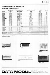
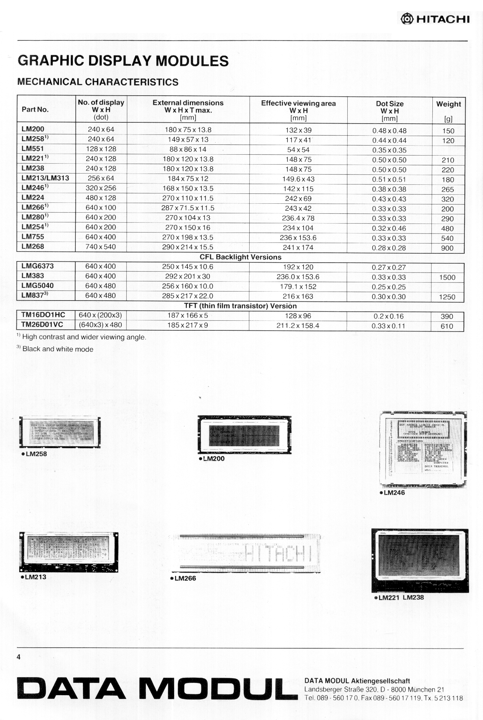
DISPLAY MODULES
MECHANICAL CHARACTERISTICS
Part No. No. of display W x H (dot) External dimensions W x H max. [mm] Effective viewing area W x H [mm] Dot Size W x H [mm] Weight [g]
LM200 240 x 64 180 x 75 x 13.5 132 x 39 0.48 x 0.38 150
LM258 240 x 64 149 x 57 x 13.5 117 x 41 0.44 x 0.44 120
LM551 128 x 128 88 x 86 x 14 54 x 54 0.35 x 0.35
LM221 240 x 128 180 x 120 x 13.8 148 x 75 0.50 x 0.50 210
LM213/LM313 240 x 128 180 x 120 x 13.8 148 x 75 0.50 x 0.50 220
LM246 320 x 256 270 x 198 x 13.5 142 x 115 0.51 x 0.38 265
LM266 480 x 128 270 x 110 x 11.5 242 x 69 0.34 x 0.33 320
LM280 640 x 200 270 x 140
Hi, die Dinger meinte ich, um konkret zu werden: https://www.ebay.com/itm/NEW-Lucent-Martek-MAX-TNT-SP-DC-H-PS2246-Power-Supply-965-W-Hot-Swappable-/132311463430 soso... schrieb im Beitrag #5259032: > Er meinte vermutlich den Einschaltpeak, verursacht durch Inrush-Ströme. Unter "Bouncen
für noch mehr > Brillanz...:-) Die alten Säcke, die sich das leisten können, hören doch nur noch max. 7KHz. Das ist die Tragik an der Geschichte.
Schrittweite 24Bit Samplerate 25usec (40KHz) Bild 1: SAW-Wellenform ca. 2031Hz mit Phasen-Jitter (max. 25usec / Div. 100µsec) Bild 2: SAW-Wellenform ca. 2031Hz mit Phasen-Jitter (max. 25usec / Div. 2msec) Bild 3: Saw-Wellenform ca. 2038Hz ohne Phasen-Jitter (Div. 100µsec) Bild 4: Saw-Wellenform
Möglichkeit zum Austausch mit anderen Gleichgesinnten war gleich null. Description The MAXIM MAX260/MAX261/MAX262 CMOS dual second-order universal switched-capacitor active filters allow microprocessor control of precise filter functions. No external components are required for a variety of bandpass
Für bestimmte HV-Teiler werden zusätzliche 10:1 Teiler benötigt, um auf modernen Oszilloskopen mit max. 10V/DIV die volle Spannung auf dem Bildschirm darstellen zu können (+/-4DIV). Derartige frequenzkompensierte Teiler für 1MΩ sind nicht kaufbar. Der Teiler ist zum Anschluß an ein Oszilloskop mit 1MΩ
Electrical Characteristics Ta= 25℃;unless otherwise specified. Symbol Parameter Test Condition Min. Typ. Max. Unit System parameters test circuit figure4 VFB Feedback Vin = 12V to 16V, Vout=18V 1.213 1.25 1.287 V Voltage Iload=0.1Ato 2A Efficiency ŋ Vin=12V ,Vout=18.5V - 92 - % Iout=2A Electrical Characteristics
Electrical Characteristics Ta= 25℃;unless otherwise specified. Symbol Parameter Test Condition Min. Typ. Max. Unit System parameters test circuit figure4 VFB Feedback Vin = 12V to 16V, Vout=18V 1.213 1.25 1.287 V Voltage Iload=0.1Ato 2A Efficiency ŋ Vin=12V ,Vout=18.5V - 92 - % Iout=2A Electrical Characteristics
UAA2080 and UAA2082 with software decoding. QUICK REFERENCE DATA SYMBOL PARAMETER CONDITIONS MIN. TYP. MAX. UNIT VDD supply voltage 1.8 − 6.0 V DDPD power-down supply current CE = V SS − 1.0 10.0 A DD operating supply current CE = V DD; note 1 − 1.5 20.0 A Pi(ref) sensitivity improvement at 3% bit error
indication Frequency Hz 50 60 Evaporating temperature °C -35 to -5 – Voltage range V 187 to 264 – Max. condensing temperature continuous (short) °C 60 (70) – Max. winding temperature continuous (short) °C 130 (130) – S = Static cooling normally sufficient Cooling requirements O = Oil cooling Frequency
ziemlich LUT-fressend dann, ist ja klar. Wieso keinen IP-Core? Die sind sehr effizient gemacht. Die max. 70% Füllgrad sind ein Erfahrungswert meinerseits. Ich hatte bisher bei allen FPGA Designs, die mehr als 70 oder 75% belegen, Schwierigkeiten beim Routing. Erstens mal dauert das dann ewig und zweitens
geringen Verlustwärme entsprechend kleiner ausfallen. Ausgangsleistung je Kanal: ........................max. 150 W an 4 Ω (<10 % THD + N) Herkömmliche Digital-Verstärker in Dauer-Ausgangsleistung:.....................................120 W an 4 Ω (<1 % THD + N) Class-D-Technologie (Pulsweiten-Modu- je Kanal
verdampfen, oder? Ja das schon, aber Du brauchst für die Lotpaste ja höhere Temperaturen. So 230-240° max. sollte es schon schaffen denke ich mal. Also erstmal sollte man vielleicht mal bei den Firmen da anfragen was deren Mini Anlagen so kosten. Wenn das >2000 Euro ist, dann lohnt sich das natürlich
Wasser als Kühlmittel, bei den Designs, die ich gesehen habe, sitzt die Kühlung gerade oberhalb der 213grad Zone, das heisst, sie begrenzt sie. Ehrlich gesagt bezweifle ich ein bisschen, ein geschlossenes System, sprich Eimer ohne Kühlkompressor (alten Kühlschrank) mit Wasser zu betreiben.
Die neue Heizung war übrigends ein totaler Schuss in den Ofen. Die Ersparnis daraus belief sich auf max. 10%, eher deutlich weniger. Was auch logisch ist, wenn man mal die Behauptungen der Heizungshersteller selber nachrechnet. Der Einfluss neuer Fenster war ebenfalls ca.10-15%, der Rest geht auf die
Instandhaltungskosten fressen die (fiktiven) Ersparnisse - siehe http://www.konrad-fischer-info.de/213baust.htm (ein bisserl scrollen ...). Vielleicht doch mal lesen? Fragt sich Konrad Fischer
a low quiescent current during USB suspend mode. The device used in the example above is a Sipex SP213EHCA which is capable of RS232 communication at up to 500K baud. If a lower baud rate is acceptable, then several pin compatible alternatives are available such as the Sipex SP213ECA , the Maxim MAX213CAI and the Analog Devices ADM213E, which are all good for communication at up to 115,200 baud. If a higher baud rate is desired, use a Maxim MAX3245CAI part which is capable of RS232 communication at rates of up to 1M baud. The MAX3245
5ms) -10 A CM P P tot Total dissipation ct T = 25°C 15 W Tstg Storage temperature -65 to 150 °C TJ Max. operating junction temperature 150 °C Table 2. Thermal data Symbol Parameter Value Unit R thj-casehermal resistance junction-case __max 8.33 °C/W 3/10 Electrical characteristics STD888T4 2 Electrical
±22.5kHz,f =1kHz m AM:f=1MHz,MOD=30%,f =1kHz m Value Parameter Symbol Test Conditions Unit Min Typ Max Supply FM mode,V =0 5.0 10.5 16.5 ICCQ in mA Current AM mode,V =0 in 3.5 5.0 8.0 F / E Quiescent QS S/N=30dB 2 uV Sensitivity Input Limiting V V 为-3 dB 2 uV IN LIM) O Sensitivity Local OSC Stop Voltage
±22.5kHz,f =1kHz m AM:f=1MHz,MOD=30%,f =1kHz m Value Parameter Symbol Test Conditions Unit Min Typ Max Supply FM mode,V =0 5.0 10.5 16.5 ICCQ in mA Current AM mode,V =0 in 3.5 5.0 8.0 F / E Quiescent QS S/N=30dB 2 uV Sensitivity Input Limiting V V 为-3 dB 2 uV IN LIM) O Sensitivity Local OSC Stop Voltage
V) Aspect: 16:10 Module Outline Size: 382.2 mm (W) x 244.5 mm (H) x 6.2 mm (D), typical 6.5 mm (D, max) and 6.2 mm (max) at the cable pass through Weight: 760 g (max), 740 g (typical) Luminance: 160 nits @ 6.0 mA (typical) Power Consumption: 6.5 W @ Black (typical, the logic plus the backlight, 6 mA
voltage 25 - 60 dc 50 - 85 Vdc 50 - 85 Vdc Rated DC voltage range 22 - 65 dc 40 – 90 Vdc 40 – 90 Vdc Max. input current 40 A 20 A 40 A Output data (AC) AC nominal power 1000 W 1000 W 2000 W Max. AC apparent power 1000 VA 1000 VA 2000 VA AC nominal current 4.3 / 8.7 A 4.3 / 8.7 A 8.7 A Rated output Voltage
process_ltbl1 ;continue with processing if length indicator >0 ret process_ltbl1: mov r16,r25 andi r25,15 ;max. length needed for 256 LEDs is 2048 bytes andi r16,$f0 sts (probability),r16 ;upper 4 bits for definition of probability in random mode elpm r16,Z+ ;read duration low byte st Y+,r16 elpm r16,Z+ ;read
www.seismologie.bgr.de/cgi-bin/eisy_test_iframe.pl?begin_date=20060101&end_date=20110314&min_lat=48&max_lat=55&min_lon=5&max_lon=15&min_mag=3.0&max_mag=9.0&submit=Erzeuge+Liste+und+Karte Ich dachte, es hätte die letzten Jahre mal irgendwo im Schwarzwald ein Erdbeben von irgendwas um die 5 gegeben. In
könn(t)en betrachte ich die Spekulation hiermit als abgeschlossen. Tsunami und Erdeben sind in max 20 Jahren wirtschftlich vergessen. Es gibt dort einfach nicht soviel Land dass Sie es sich leisten könnten einen größeren Teil davon aufzugeben. Aber genau das wird sehr wahrscheinlich geschehen.
types o 2.54mm pitch, 7.5mm long standard o 2.00mm pitch, 3.68mm long low profile • Component heights max. 1.4mm on connector side max. 1.4mm on flash side • Weight (max.) 5g Figure 2: Mechanical Dimensions for U-500 1GB-4GB drive Figure 3: Mechanical Dimensions for U-500 8GB-32GB drives All dimensions
Philips Semiconductors Product specification NPN power transistor BD329 FEATURES PINNING • High current (max. 3 A) PIN DESCRIPTION • Low voltage (max. 20 V). 1 emitter 2 collector, connected to metal part of APPLICATIONS mounting surface 3 base • Especially for battery equipped applications. DESCRIPTION handbook
Zeit pro Funktionsaufruf ist begrenzt auf 262.14 ms / F_CPU in MHz (im Beispiel: 262.1 / 3.6864 = max. 71 ms) Daher wird die kleine Warteschleife mehrfach aufgerufen, um auf eine längere Wartezeit zu kommen. Die zusätzliche Prüfung der Schleifenbedingung lässt die Wartezeit geringfügig ungenau werden

 Bild
Bild
 Bild
Bild