which 0.18 V can store up to 10 keys with overflow wrap capability. • Latch-Up Performance Exceeds 200 mA Per An interrupt (INT) output can be configured to alert JESD 78, Class II key presses and releases either as they occur, or at maximum rate. • ESD Protection Exceeds JESD 22 on all 18 GPIO Pins
Contiuous D ain Current (J= 175 °C) ID TA= 25 °C 21.8b, A TA= 70 °C 18b, c Pulsed Drain Current DM 200 Avalanche Current Pulse I 39 L = 0.1 mH AS Single Pulse Avalanche Energy E AS 94.8 mJ TC= 25 °C 50a, e Continuous Source-Drain Diode Current IS b, c A TA= 25 °C 3.13 T = 25 °C a C 100 TC = 70 °C 75
Harald W. schrieb im Beitrag #7784775: > Selber bauen mit dem L200-IC? Geht nicht auf 0V und Stromreglung instabil, weit schlechter als 1mA. Eher LT3081 oder LT1970A.
udp3305s-dc-power-supply?pr_prod_strat=use_description&pr_rec_id=948725755&pr_rec_pid=8761704841560&pr_ref_pid=8761704907096&pr_seq=uniform Das kann das. Ich habe das UDP3305S-E, das hat aber 10mV Auflösung, wenn dir das reicht, das ist gut 200 Euro günstiger.
. Siehe hier: https://www.amazon.ca/M12x1-5-10-Venting-STG-12-Breather-100-Pieces/dp/B08FFVM5F7/ref=sr_1_4? Gerhard
Beitrag #7784750: > https://www.amazon.ca/M12x1-5-10-Venting-STG-12-Breather-100-Pieces/dp/B08FFVM5F7/ref=sr_1_4? Einen Beutel mit 100 Stück für fast 200 € will sich vielleicht deswegen nicht jeder hinlegen. Noch ist die Schutzart des Gehäuses gar nicht klar.
in order to insure stability. The waiting time period for PT2257 to send I C Bus Signal is at least 200ms. If the waiting time period is less than 200ms, I C Control may fail. Please refer to the diagram below. V1.5 5 March 2013 PT2257 DATA BYTES DESCRIPTION FUNCTION BITS MSB 2 3 4 5 6 7 LSB Function
with wet hands. • Do not open the casing of the power supply when it is connected to ac mains. • Refer all servicing to qualified service personnel only. • Before replacing the AC fuse at AC socket, find out and clear up the cause first. • Replace the AC fuse with the same type and rating as the original
falsch angeschlossen? Und dann zu den Takten: Beide sys_clk_i bekommen aktuell 166.666 MHz, die clk_ref_i ist mit einem 200 MHz Takt verbunden. Beide Takte kommen aus einer PLL im Toplevel. Mich verwirrt im MIG die Einstellung von Takten ohne Angabe in welchem Zusammenhang die mit den Port stehen.
angeschlossen? > Und dann zu den Takten: > Beide sys_clk_i bekommen aktuell 166.666 MHz, die clk_ref_i ist mit > einem 200 MHz Takt verbunden. Beide Takte kommen aus einer PLL im > Toplevel. Mich verwirrt im MIG die Einstellung von Takten ohne Angabe in MIG sollte den system clock von externen
Non Inductive Aryton-Perry Mechanically style available upto 1K0 Crimped Termination Assembly AEC-Q200Qualified e : info@htr-india.com www.htr-india.com Rev Date : 22/05/2019 PHYSICAL CONFIGURATION WIRE WOUND RESISTORS CERAMIC ENCASED TYPE HEA HTR POWER DIMENSIONS (mm) RESISTANCE TYPICAL TYPE RATING *
Content: < 0.3g Operating Temp: -30C to 60C Self Discharge: ~1% / year 24.50 (0.965) 3.45 (0.136) Ref. 24.30 (0.957) 3.15 (0.124) Ref. Safety: R1.25 (0.049) Ref. 22.0 (.866) 1.00 (0.039) Ref. Max Minimum (1) KEEP OUT OF REACH OF CHILDREN. Swallowing may lead to R0.75 (0.030) Ref. serious injury or death
nummerieren, und dann mit einem Textfile als Ergänzung als Inhaltsverzeichnis erstellen. <a href="#fn200" class="footnote-ref" id="fnref200" role="doc-noteref"><sup>200</sup></a></p> <h2 id="np-r.-samweis-1"> Np R. (samweis) </h2> <p>Wer etwas in der Birne hat, der kann die offizielle Abkürzung verwenden
main power button for 3 seconds to turn off. APP Note: The figures are for reference only. Please refer to the actual APP interface. Use the ShinePhone application to remotely monitor and control your Noah 2000 Balcony Solar Storage system. Support 2.4G WiFi only. Create A Power Plant 1. Scan the QR
Charge AC Charging Cable X-Stream Fast Charging 900W Max input Power Customized Charging Power Range: 200-900W (Default : 200W) English edition EcoFlow APP The charging power can be adjusted through the AC Charge Speed Switch on the back of the product. You can set the charging power range in the EcoFlow
CHARACTERISTICS (Note 3) PARAMETER CONDITIONS MIN TYP MAX UNITS Zero Input Reading VIN = 0V, full scale = 200.0mV -000.0 000.0 +000.0 Digital Reading Ratiometric Reading V = V , V = 100mV 999 999/1000 1000 Digital IN REF REF Reading Rollover Error (Difference in Reading for Equal Positive and Negative Reading
dass der Shop angeblich nur 50 Geräte hatte und alle der geschätz 200 Personen somit nur Vorbestellungen abgeben konnten und Anzahlungen leisten durften. Ein anderer Shop hat ähnlich verfahren, Anzahlungen kassiert und dann den Laden zugesperrt: Er stand schon kurz vor
Laufwerken > (Ultrasearch) Das hier war bei mir am schnellsten: http://www.master-seeker.com/?ref=uiabout
Laufwerken > (Ultrasearch) Das hier war bei mir am schnellsten: http://www.master-seeker.com/?ref=uiabout Sherlock 🕵🏽♂️ schrieb im Beitrag #7777096: > Peter D. schrieb: >> Die Suche im Explorer funktioniert wie immer. > > Wie immer nicht zuverlässig. Manchmal findet sie Dateien nicht,
ZCD rise ZCD Threshold Voltage 2 V zcd2 0.55 0.67 0.79 V ZCD drop Minimum Detection Pulse T zcd1 100 200 - ns Width ZCD Output Delay T zcd2 - 260 520 ns Input Clamp Voltage (High) V ih 6.1 6.7 7.3 V Isink=3mA Input Clamp Voltage ( Low) V il -0.3 -0.1 - V Isource=-3mA [ Restart Block ] Restart Time TRS
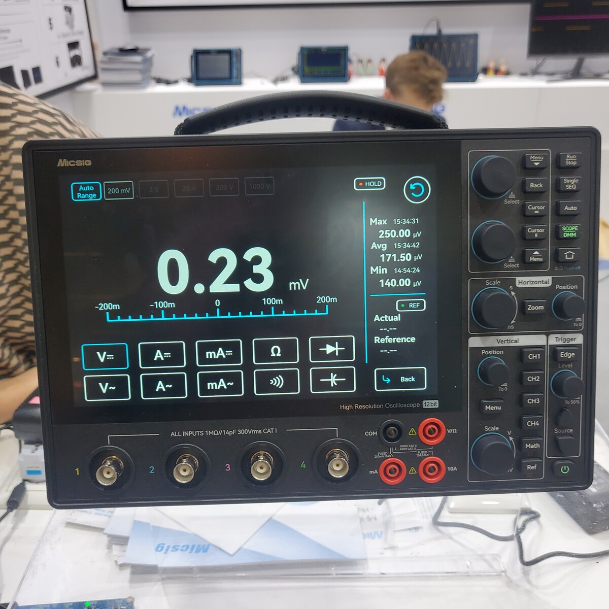
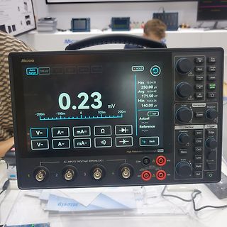
MICSIG Auto Range 200 mV 2 V 20 V 200 V 1000 V HOLD 0.23 mV -200m -100m 100m 200m Max 15:34:31 Avg 250.00 15:34:42 171.50 Min 15:44:24 140.00 V= A= mA= Ω Diode ⟳ V~ A~ mA~ ⟳ Reference Actual Scale Horizontal Position Zoom Menu Back Vertical Position CH1 Edge CH2 To 50% CH3 To 50% CH4 Source Math Ref 1 2 3 4 COM V/Ω High Resolution Oscilloscope 12bt
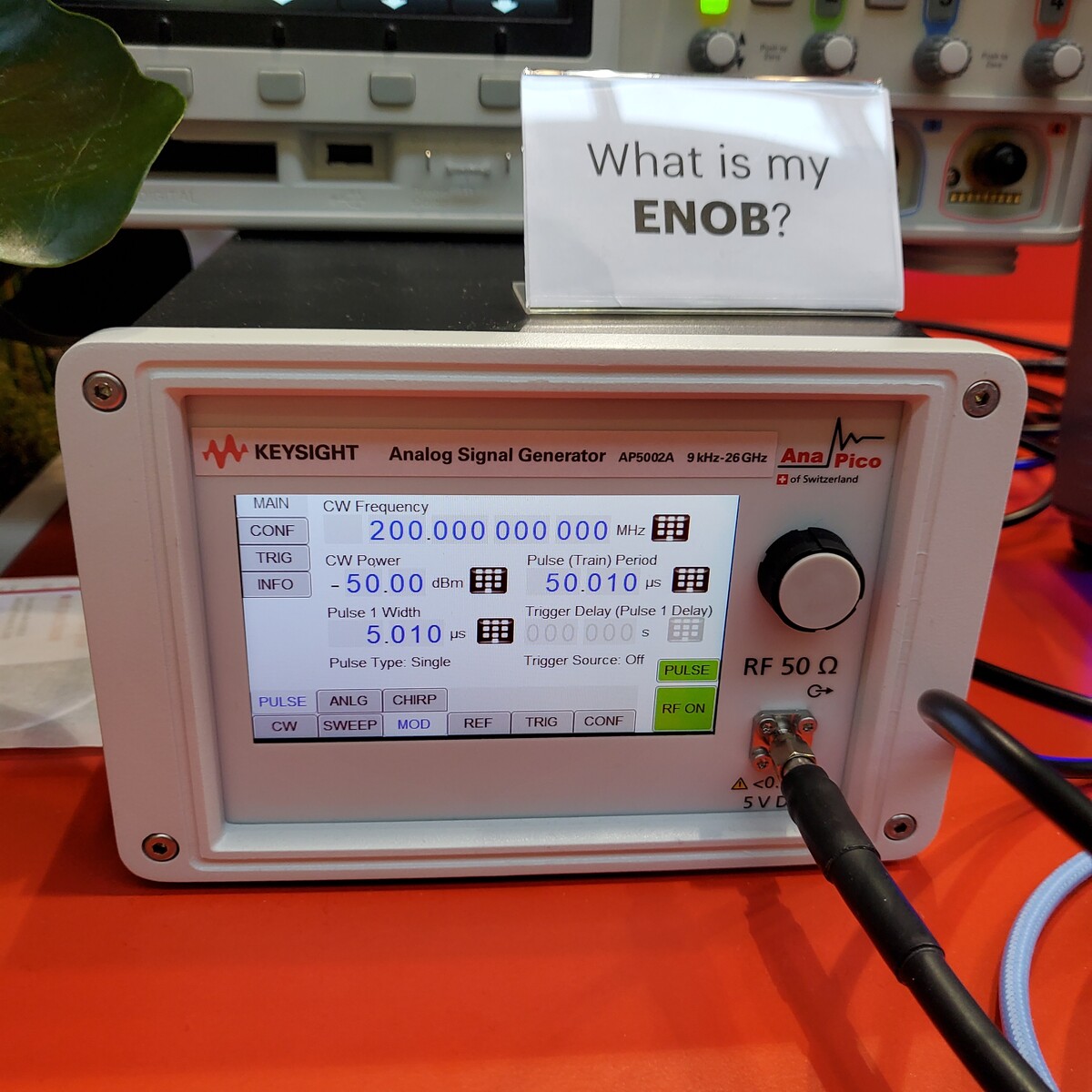
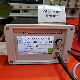
ENOB? KEYSIGHT Analog Signal Generator AP5002A 9 kHz-26 GHz Ana Pico of Switzerland MAIN CW Frequency 200.000 000 MHz CONF CW Power - 50.00 dBm 50.010 µs TRIG Pulse(Train) Period INFO Trigger Delay (Pulse 1 Delay) 0.000 s Pulse 1 Width 5.010 µs Pulse Type: Single PULSE ANLG CHIRP REF TRIG CONF RF 50 Ω
. Gate Voltage Fig 13. Typical On-Resistance vs. Drain Current 600 500 ) W r 400 e o P s 300 u P l 200 i S 100 0 1E-5 1E-4 1E-3 1E-2 1E-1 1E+0 Time (sec) Fig 14. Typical Power vs. Time Driver Gate Drive P.W. D.U.T + P.W. Period D =Period V =10V CircuitLayoutConsiderations GS • Low Stray Inductance •
For example, if all outputs are programmed to turn on for 1ms, but the BLANK signal is only low for 200ns, all outputs still turn on for 200ns, even though some outputs are turning on after the BLANK signal has already gone high. Table 3. BLANK Signal Truth Table BLANK OUT0 - OUT15 LOW Normal condition
action. In some cases the default properties may be acceptable and no modification is necessary. Refer to Section “5. Commands and Properties” for a full description of each command and property. Table 34. Programming Example for the FM/RDS Receiver Action Data Description Powerup in Digital Mode CMD
On-Off Ratio 30 i a 20 n t 15 e 15 d 0 f i 0 4 8 Gray-shade data24 28 n DC[4] Green Enhance Mode. Refer to command Set Color Mode for more information. 0b: Green Enhancing Mode enabled 1b: Green Enhancing ModeCdisabled N1. For red and blue colors, when PWM is off, the shades mapped to data 1 and 30 (
Product complies to MSL Level 2 acc. to JEDEC J-STD-020E OHA04525 300 ˚C T 250 T 245˚C 240˚C p t 217˚C P 200 t L 150 S 100 50 25˚C 0 0 50 100 150 200 250 s 300 t Profile Feature Symbol Pb-Free (SnAgCu) Assembly Unit Minimum Recommendation Maximum Ramp-up rate to preheat *) 2 3 K/s 25 °C to 150 °C Time t t
Continuous Drain CurrentGSV@ -10V -52 A DM Pulsed Drain Current -260 PD@T C 25°C Power Dissipation 200 W Linear Derating Factor 1.3 W/°C V Gate-to-Source Voltage ± 20 V GS EAS Single Pulse Avalanche Energy 930 mJ AR Avalanche Current -38 A E Repetitive Avalanche Energy 20 mJ AR dv/dt Peak Diode Recovery
For the mapping between INTERRUPT_CORE0_INTR_STATUS_n_REG and peripheral interrupt sources, please refer to Table 8-1. Espressif Systems 200 ESP32-C3 TRM (Version 1.1) Submit Documentation Feedback s 8 r 8.4 Register Summary I s e f r S The addresses in this section are relative to the interrupt matrix
voltage 4.2V Power off save: save settings parameters only, do not save measurement data Product weight: 200g (net weight) 260g (including packaging) Product size: 150 × 103 × 36mm Packaging size: 182 × 112 × 50mm Hardware introduction 1. Type-C5V power supply interface 2, Type-C5V power supply interface 3
. (*) Available on Request. Figure 3: Test Circuit Table 4: Electrical Characteristics Of L7905C (refer to the test circuitsJ T 0 to 125°C, VI= -10V, I = 500 mA, C = 2.2 µF, C = 1 µF unless otherwise specified). O I O Symbol Parameter Test Conditions Min. Typ. Max. Unit VO Output Voltage T J 25°C -4.8
Equipment LM7805 is also available in a higher accuracy and better performance version (LM340A). Refer to • Brushed and Brushless DC Motor Drivers LM340A specifications in the LM340A Electrical • Solar Energy String Invertors Characterisitcs table. SPACE (1) Device Information Available Packages PART
Hand. Ach so, vielleicht nochmal einen Link auf das Zeug: https://www.amazon.de/dp/B0BHNRY2WD?ref=ppx_yo2ov_dt_b_fed_asin_title Finde ich sogar erstaunlich preiswert! Vanye
den immer nur so hoch wie unbedingt nötig, um einen möglichst gleichmäßigen Fluss hinzubekommen. 200mm/s für den Eilgang ist okay. Halt so viel, wie der Drucker schafft. Wie gesagt, die Stahldüsen halten besser, leiten aber die Wärme nicht so gut wie Messingdüsen. Mit den Rubindüsen habe ich noch
Description SCL 6 serial clock line SDA 7 serial data line VDD 8 supply voltage 6. Functional description Refer to Figure 1 ÒBloc k diagram of PCA9533Ó . 6.1 Device address Following a START condition, the bus master must output the address of the slave it is accessing. The address of the PCA9533/01 is shown
Sample/Hold Capacitor C — 30 — pF SAR Input Mux Impedance R MUX — 5 — kΩ Voltage Reference Range V REF 1 — VDD V Input Voltage Range V IN Single-Ended (AIN+ - GND) 0 — V REF V Differential (AIN+ - AIN-) -V — V V REF REF Power Supply Rejection Ratio PSRR ADC — 70 — dB DC Performance, VREF = 2.4 V Integral
accompany this product. They contain important information on setting up and using the device. You should refer to these instructions, even if you are buying this product for someone else. Please retain these Operating Instructions for future use! A list of the contents can be found in the Table of contents,
Material das sonst in die Tonne fliegen würde. Von den Senseo-Schachteln habe ich mittlerweile über 200 Stück in denen in ich mein Material verstaue. Natürlich musste ich meine Regale etwas umbauen und Zwischenböden einbauen. Gruß Ralf
werden. Ich meine mich zu erinnern, dass es einen gängigen billig-OPV mit integrierter Bandgap ref gibt. Oder ein negativer Spannngsregler kann entsprechend zweckentfremdet werden. Ein einfacher PMOS-FET hat leider eine starke temperaturabhängigkeit in VGS, das könnte man natürlich kompensieren
Mindestensstrom des TLE unterschritten. ADC Eingang highside? Bss hat einen Leck Strom, der bei 200k Last deutlich stören wird.
comparative table with numbers on illustrated parts breakdown) (NOTE) Please use the following table to refer the numbers shown on illustrated parts breakdown Part Code Parts Name Location Reference QTY Code# 530000000315 SP250 PIANO STANDɹPART 1 12SP250HX0Y Assembled 530000000316 SP250 MUSIC STAND,HIPS 428C
Current Limit 4.0 4.7 A COMP to Current Sense G CS 9 A/V Transconductance Error Amp Voltage Gain5) 200 V/V Error Amp Transconductance ICOMP= ±3µA 40 60 80 µA/V Error Amp Min Source current V FB= 0.7V 5 µA Error Amp Min Sink current V FB= 0.9V –5 µA VIN UVLO Threshold 2.7 3.0 3.3 V VIN UVLO Hysteresis
CurrenA (T = 55 °C) F(AV) 200 300 mA Peak Forward Surge Current 8.3 ms Single Half Sine-Wave I 2 A Superimposed on Rated Load (JEDEC Method) FSM Operating Temperature Range TJ -40 to +125 °C Storage Temperature Range T -40 to +125
2.0V n V I:2.0V i VI:1.5V i V I:1.5V i 40 i 40 E E 20 20 0 0 0 200 400 600 800 0 200 400 600 800 Output CurrentOUT(mA) Output CurrenOUT(mA) 3) Ripple Voltage vs. Output Current R1210N302C R1210N302D L:27μH L:27μH )280 )280 V V (240 (240 l l VI:1.5V p200 V I:1.5V p200

 Bild
Bild
 Bild
Bild
 Bild
Bild
 Bild
Bild