0x800500 -Wl,--defsym=__DATA_REGION_LENGTH__=32768[/c] angegeben werden. Dieselbe Software für den AT90CAN128 funktioniert aber auch mit der Version 4.3.3. Hier ist jedoch kein externer Ram angeschlossen und auch nicht beim Linken eingestellt, weil der genug internen hat. Es wird also Zeit, dass ich
software; you may redistribute it under the terms of the GNU General Public License version 3 or (at your option) a later version. This program has absolutely no warranty. [/pre] Schwieriger ist es für die AVR-LibC, da es für diese keine installierten ausführbaren Kommandos gibt. Hier musst du
bei mehreren Projekten im Internet zu finden. Ich habe lediglich die Timerinitialisierung für den AT90CAN128, ATMega162 und AT90S8515 geändert. Bei allen drei Controllern läuft es einwandfrei. Sowohl auf einem STK500 als auch STK200. Beim STK200 aber mit zusätzlichem RAM. Ausserdem ist es nur schwer
/c] Nach kurzem Nachdenken fiel mir auf, dass ich als Parameter beim Compiler und Linker "-mmcu=at90can128" angegeben hatte, die Software aber mittlerweile für den AT90CAN128 zu gross ist, was den Ram betrifft. Beim Compilieren für den ATMega2560 war die Meldung nicht. Das Ganze nochmal getestet
electrolytic capacitors, switching current, it requires an adequate ripple the ESR dominates the impedance at the current rating. The RMS current in the input switching frequency. For simplification, the capacitor can be estimated by: output ripple can be approximated to: VOUT ⎜ VOUT ⎟ ∆V = VOUT ×⎛1− VOUT ⎞×
circuitry Choose an inductor that will not saturate under the maximum inductor peak current. The peak can be seen at the output when the MP1584 is at no load. In order to absorb this small amount inductor current can be calculated by: of current, keep R2 under 40KΩ. A typical value for R2 can be 40.2kΩ.
voltage ripple low. The output voltage the output resistor of tPe error amplifier, and the ripple can be estimated by: M other is due to the output capacitor and the load VOUT V OUT 1 VOUT R OSR 1 resistor. These poMes are located at: fS L VIN 8 f S C2 D P1 2C3 AA Rhereis
Voltage Tolerance Note.3±1.0% Line Regulation ±0.5% Load Regulation ±0.5% Setup, Rise Time 800ms, 60ms at full load Hold Up Time (Typ.) 16ms / 230VAC at full load Voltage Range Note.490 ~ 264VAC, 127 ~ 370VDC Frequency Range 47 ~ 63Hz Power Factor (Typ.) 0.98 / 230VAC, 0.99 / 115VAC at full load Input Efficiency
sleep mode, only the calibrated real-time clock and watchdog remains active. The real- time clock can be programmed to wake up the ESP8266 at any required interval. The ESP8266 can be programmed to wake up when a specified condition is detected. This minimal wake-up time feature of the ESP8266 can be
CE SELECTION GUIDE In the R1210N Series, the output voltage, the oscillator frequency for the ICs can be selected at the user’s request. The selection can be made by designating the part number as shown below; Product Name Package Quantity per Reel Pb Free Halogen Free R1210Nxx2-TR-FE SOT-23-5 3,000
is arailable in nals or will deliver 20 mA output current with 0.4V the limited temperature ranges at a cost savings. a tion. Reference output can be as low as 200 mV. n The circuit is recommended for portable equipment anFeatures d completely specified for operation from a single power cell. V In contrast
retriggering (nA) or (nB). By repeating this process, the output pulse period (nQ = HIGH, nQ = LOW) can be made as long as desired. When nRD is LOW, it forces the nQ output LOW, the nQ output HIGH and also inhibits the triggering. Schmitt-trigger action in the nA and nB inputs, makes the circuit highly
monostable multivibrator. Each multivibrator features edge-triggered inputs (nA and nB), either of which can be used as an enable input. Pulse triggering occurs at a particular voltage level and is not directly related to the transition time of the input pulse. Schmitt-trigger input circuitry for the nB inputs
Karl K. schrieb im Beitrag #7754049: > Statt 90 Watt ist > der Eigenverbrauch des Wechselrichters dann nur noch 70Watt. das heißt für den Eigenverbrauch zieht er sich in 12h mehr als 1kWh aus dem Akku? Ganz schön viel.
den WR dazu, dass er mir Registerdaten > zurückschickt? Du könntest mit einigen Befehlen aus dem AT-Befehlssatz experimentieren, ob überhaupt etwas beantwortet wird. Aber pass auf, dass Du dabei nicht irgendwas verstellst. https://de.wikipedia.org/wiki/AT-Befehlssatz
www.mikrocontroller.net/topic/244442#2683557 Da kann sich Günter jetzt mal reinwühlen. Da hat er zu tun bis er über 90 ist.
Hier der Grund, wieso es nur um "ein" Bit ging. "...By logic level at the input S you can change the polarity of the segment outputs accordingly to the displays with common anode or cathode. Logical One for common anode displays, logical Zero for common cathode displays
Junction temperature T -40 – 150 °C – J Storage temperature range TSTG -65 – 150 °C – 1) ESD capability at all pins VESD HBM – – 2 kV HBM acc. to JESD22 - A114 1) Two different classes of ESD protection elements are implemented within ILD6150: 1. ESD protection at pin VS will be triggered if the voltage at
Warning The minimum timer period is one millisecond in MicroPython, whereas with Arduino code, it can easily be reduced to one microsecond. Timer performances are limited so that MicroPython can keep up with the pace.. Damit ist die Methode "Timer" aus "Machine" gemeint. Also fast sowas wie ein Abstraction
MeanTime toFailure (MTTF) Discharge (ESD) Sensitivity Nominal JunctionTemperature (T = 85°C, 187 Stresses at or above those listed under Absolute Maximum V DD= 50V) ESDCAUTION Ratings may cause permanent damage to the product. This is a stress rating only; functional operation of the product at these or any
Information (1) PART NUMBER PACKAGE BODY SIZE (NOM) • USB Ports and Hubs • Digital TVs TPS2552 SOT-23 (6) 2.90 mm x 1.60 mm WSON (6) 2.00 mm x 2.00 mm • Set-Top Boxes SOT-23 (6) 2.90 mm x 1.60 mm • VOIP Phones TPS2553 WSON (6) 2.00 mm x 2.00 mm (1) For all available packages, see the orderable addendum at the
TO252-3L and SOT223-3L are +12°C/W and +16°C/W respectively. Thermal resistances from tab to ambient can be as low as +30°C/W. The total thermal resistance from junction to ambient can be as low as +42 to +46°C/W. This requires a reasonable sized PCB with at least one layer of copper to spread the heat
SRAM 0 in Section 3.3.2). The uniform cache is accessible by the instruction bus and the data bus at the same time, but can only respond to one of them at a time. When a cache miss occurs, the cache controller will initiate a request to the external memory. Espressif Systems 91 ESP32-C3 TRM (Version
Taped acc. to AC05-AT GC GC 500 IEC 60286-2 on reel - 12.7 mm 365 mm x 370 mm x 67 mm AC05-NI AC07 Taped acc. to IEC 60286-1 AC07-AT AC AC 500 fan-folded in a box 73 mm 10 mm 265 mm x 90 mm x 118 mm AC07 DK/EK LB LB 250 Bulk
isheldbelow2.0V;theoutputsaretri-statedifV PP is held above 2.0 V. FLASHlogic device configuration data can be reloaded from FLASH Power-On memory at any time by issuing a JTAG RESET instruction. For EPX880 Reset (POR) andEPX8160devices,thedeviceconfigurationdatafromFLASHmemory can also be reloaded by holding PP at a logic low (0.8 V maximum) for a minimum of 300 ns. By holding V PP low during power-up, the power-up cycle can be delayed. The power-up cycle is completed within a delay of RESET afterV PPreaches2.0V
the clock can be stopped – Power-down mode without loss of user data and then the execution resumed from the CMOS and TTL compatible point the clock was stopped. TWO speed ranges at V CC = 5V SELECTION TABLE – 0
recalibrate its internal tuning circuitry, forcing the output clock to momentarily stop and start at any arbitrary point during a clock cycle. This re-calibration process establishes a new center frequency and can take up to 10 ms. Circuitry receiving a clock from the Si57x device that is sensitive
in eine große, umständliche Schaltung, die unötig teuer ist, lange zur Fertigstellung braucht, zu 90% aus überdesignten Komponenten besteht und daher äußerlich nach rocket science ausschaut, dann aber irgend eins der anderen 10% Restbauteile infolge von Fehlplanung und nichtdurchdachtem Konzept die
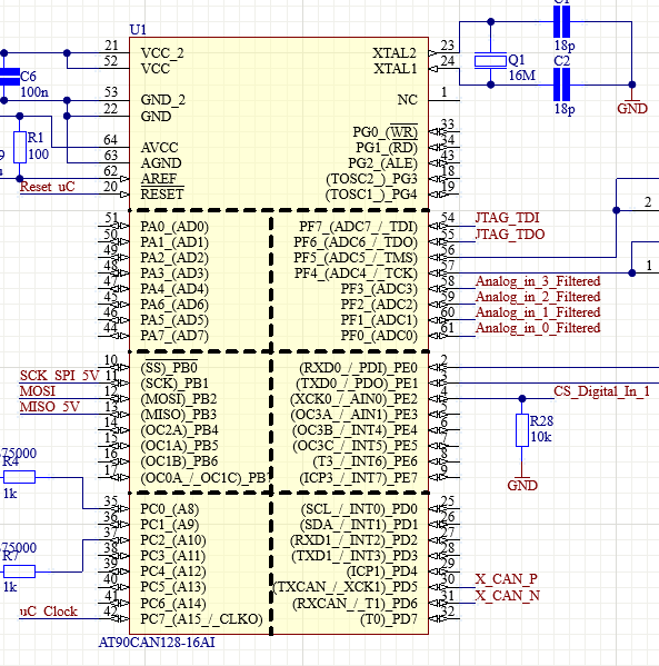
Max schrieb im Beitrag #7750080: > AT90CAN128.PNG > ATmega16.PNG An _jedem_ VCC Pin _ein_ Abblock-Kondensator gegen Masse. An _jedem_ ! Max schrieb im Beitrag #7750080: > aus dem Schaltplan mit rangehangen. Nein! .... aus
Slave-Programm wurde original doch gar nicht übersetzt!?) läuft es hier (mutatis mutandis), mangels AT90CAN zwischen zwei ATmega16.
output ON, l = 100 mA — 1.0 mA DD OUT All outputs OFF — 50 µA Output Rise Time t l = 100 mA, 10% to 90% — 500 ns r OUT Output Fall Time t l = 100 mA, 90% to 10% — 500 ns f OUT NOTE: Positive (negative) current is defined as going into (coming out of) the specified device pin. TRUTH TABLE Serial Shift
for ‘‘Operating Temperature Range’’, they are not meant to imply that the devices should be operated at these limits. The table of ‘‘Electrical Characteristics’’ provides conditions for actual device operation. Note 2SSVe0V unless otherwise specified. Note 3OHIandOLare tested one output at a time. 2 DC
Event-Loop enthählt (Windows, STM32 oder nRF52). Hier ein github-Link: https://github.com/Jochen0x90h/coco-loop/blob/main/test/LoopTest.cpp Monochome Displays gehen auch schon: https://github.com/Jochen0x90h/coco-mono-display sowie Funkübertragung mit nRF5284. Es gibt eine ganze Reihe von coco-Bibliotheken
das müsste man mit dem > Compiler Explorer mal genauer untersuchen. The call to operator new can be optimized out (even if custom allocator is used) if The lifetime of the coroutine state is strictly nested within the lifetime of the caller, and the size of coroutine frame is known at the call
more space on the screen is desired, this option can be chosen to hide the toolbar. Selecting it a second time will show the toolbar again. It may be useful to note that the toolbar can be undocked from the main screen and made to “float” at a user-defined
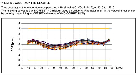
7.3.2.TIME ACCURACY 1 HZ EXAMPLE
Time accuracy of the temperature compensated 1 Hz signal at CLKOUT pin, TA = -40°C to +85°C:
The following curves are with OFFSET = 0 (default value on delivery). Fine adjustment in the vertical direction can be done by determining an OFFSET value (see AGING CORRECTION).
4
3
2
1
0
-1
-2
-3
-4
ΔF/F [ppm]
-50
-40
-30
-20
-10
0
10
20
30
40
50
60
70
80
90
TA[°C]
and “Black” state. Time ON (TON) is the time between photo detector output intensity changed from 90% to 10%. And time off (TOFF) is the time between photo detector output intensity changed from 10% to 90%. DWIN Technology 15 www.dwin-global.com LI10600T070IA3098_datasheet Professional, Creditable,
and “Black” state. Time ON (TON) is the time between photo detector output intensity changed from 90% to 10%. And time off (TOFF) is the time between photo detector output intensity changed from 10% to 90%. Note 5: Definition of color chromaticity (CIE1931). Color coordinates measured at center point
memory (RAM) also provides 100 instrument settings. Any one of the nonvolatile instrument settings can be selected as the power-up setting for the instrument. Memory cloning The stored settings in one instrument can be easily transferred (without the use of a controller) to another instrument using
interface. https://www.eevblog.com/forum/repair/quick-repair-project-marconi-2024/?all da wird ein AT28C256 erwähnt, kann aber sein, dass es dabei um den 2025 geht. Und ein Level2-Passwort, wie man es herausfindet (2025?) Hier ein Foto der Rückseite, aber ohne Batteriehalterung: https://www.rigpix.com
to a vibration table directly and subjected to vibration that consists of 10 Hz to 55 Hz to 10 Hz at the speed of 1Hz/min in 90~100 mins.The total excursion of the vibration is 0.8 mm (0.060 inches). The cell shall be 5.5.1 Vibration testNo leakage vibrated in each direction along axis of the cylinder
DD - AVR DU Interessant wäre für meine Anwendungen, ob überhaupt und welche davon mit (wieviel) CAN sind.
JTdCJTIyY2F0ZWdvcnlkcm9wZG93biUyMiUzQSU1QiUyMk1pY3JvY29udHJvbGxlcnMlMjBhbmQlMjBNaWNyb3Byb2Nlc3NvcnMlMjIlMkMlMjIlMjIlMkMlMjIlMjIlNUQlN0Q= Schade, nur die beiden bisherigen Typen mit nur einem CAN (AT90CAN*, ATmega*M1).
timeout periods (Table 1). Timeout settings of 100ms. This output structure sinks current when WDO can be hard wired, or they can be controlled with logic is asserted. Connect a pullup resistor from WDO to any gates and modified during operation. To ensure smooth supply voltage up to +5.5V. transitions
Steckdose geklebt wurden und die Löcher abdeckten. Um den Stecker reinstecken zu können, mußte man ihn 90° gedreht ansetzen, 90° drehen und reindrücken. Rainer Z. schrieb im Beitrag #7739662: > Ich war vermutlich weniger gehorsam oder die Neugier überwog. Vielleicht lag es auch daran, daß mein Vater
Computer Most latency problems do not result from electricity. However, rarely, they do. It's often at the level of "Too infrequent to show up in manufacturer beta testing" but at the level of "It appears over a thousand people are affected in a population of 10,000,000" "Latency from interference
RFI 309 µm 1436 µm Power Supply Ground VSS 16 µm 1415 µm Notes: 1) OUT = VSS when carrier amplitude at maximum; OUT = VDD when carrier amplitude is reduced (modulated) - the output is a current source/sinOUT > 5 µA - at power down the output is high impedance 2) AON = VSS means AGC off (hold current gain
determined by the move source seg start and move source seg end parameters. The destination byte segment can be at any byte position of a doubleword. • Minimum source segment start address of a chapter is row/column = 0/0. Maximum source segment start address of a chapter is row/column = 25/23. Minimum source
loader then determines if the device should stay in bootload mode or jump to the reset vector located at 0x0000. When the bootloader is not present, the device will jump to the reset vector of 0x0000 after any reset. More information about the bootloader protocol and usage can be found in AN945: EFM8 Factory
channels deselected temperature sensors are needed in the application, • Low R ON switches one sensor can be connected at each channel: 0-7. • Allows voltage-level translation between 1.8-V, The system master can reset the TCA9548A in the 2.5-V, 3.3-V, and 5-V buses event of a time-out or other improper
mit dem Skalarprodukt. Die Formel mit der Kräftezerlegung ist seltsam, da [math]\alpha + \beta = 90[/math] ist ja, [math]180-90=90[/math] und [math]\sin 90° = 1[/math].
the DTE and the M1306B (DCE), Check the configuration of the port COM used on the DTE. • Example of AT commands which can be used after getting started the M1306B: AT+CGMI : M1306B answer is "WAVECOM MODEM" when serial link is OK. AT+CPIN=xxxx: to enter a PIN code xxxx (if activated). AT+CSQ : to verify
from 4.5 V to 24 V supply voltage changes to the previous edition. – switching offset compensation at 62 kHz – overvoltage protection 1. Introduction – reverse-voltage protection at DD -pin The HAL300 is a differential Hall switch produced in CMOS technology. The sensor includes 2 temperature- – short-circuit
Industrial Automation Glossary A glossary of industrial automation terms and AG-7.1 abbreviations. You can view or downloadpublications at http://www.rockwellautomation.com/literature/.Toorderpapercopiesof technicaldocumentation,contactyourlocalRockwellAutomationdistributoror salesrepresentative. Youcandownload

 Bild
 Bild