-
Datei
Picoscope.txt
(Endpoint Descriptor) bEndpointAddress : 0x01 (Direction=OUT EndpointID=1) bmAttributes : 0x02 (TransferType=Bulk) wMaxPacketSize : 0x0200 (max 512 bytes) bInterval : 0x00 (never NAKs) Data (HexDump) : 07 05 01 02 00 02 00 ....... ----------------- Endpoint Descriptor ----------------- bLength : 0x07
in „Reparatur Picoscope 2203“ · Mikrocontroller und Digitale Elektronik ·
-
 Bild
Bild
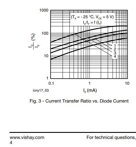
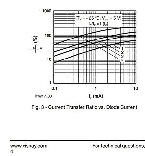
Kennlinie Current Transfer Ratio vs. Diode Current
1000 (TA = - 25 °C, VCE = 5 V) IC/IF = f (IF) 100 10 1 0.1 1 10 IF (mA) icny17_03 Fig. 3 - Current Transfer Ratio vs. Diode Current www.vishay.com For technical questions, 4
in „Netzspannungserkennung gesucht, möglichst stromsparend“ · Haus & Smart Home · · Screenshots
-
Datei
anders.txt
) { if ((QM_Enabled == 1) || (Cursor_Enabled == 1)) { TransferDataPlane_asm_persistant(0x008DBB24, 0x00970F30); //BF del -> pixel error } else { TransferDataPlane_asm_persistant(0x008DC254, 0x00971660); //BF -> fixed by Guido } //TransferDataPlane_asm_persistant(0x008DC254, 0x00971660); //BF -> fixed by Guido } Dasselbe Spiel in TransferDataPlane_asm_persistant: void Hardware::TransferDataPlane_asm_persistant(unsigned long Buffer_Adr1, unsigned long Plane_Adr1) { if ((QM_Enabled == 1) || (Cursor_Enabled == 1)) { asm(" PFX %hi(1460
in „Wittig(welec) DSO W20xxA Open Source Firmware“ · Mikrocontroller und Digitale Elektronik ·
-
Datei
readsend.cpp
; // signalisation of a remote transfer request } else { dataIn[0] = READ_RX_BF00; //read the SIDH and SIDL registers of BF0 SPIRW pID->stdID = (dataOut[1] << 3) | (dataOut[2] >> 5); //write identifier into the address *dataLength = (int
in „Mit MCP2515 CAN-Bus-Daten auslesen“ · Mikrocontroller und Digitale Elektronik ·
-
Datei
BEISPIEL.c
************************************************ Issues a start condition and sends address and transfer direction. If device is busy, use ack polling to wait until device is ready Input: address and transfer direction of I2C device ********************************************************************
in „Expander: Digitaleingänge“ · Mikrocontroller und Digitale Elektronik ·
-
Datei
twimaster.c
************************************************ Issues a start condition and sends address and transfer direction. If device is busy, use ack polling to wait until device is ready Input: address and transfer direction of I2C device ********************************************************************
in „I2C Übertragungsproblem“ · Mikrocontroller und Digitale Elektronik ·
-
Datei
ReleaseNote.txt
and prototyping/development, but is not suitable for production usage on remote devices. 4. File transfer over WebREPL has additional issues, usually triggered when transferring large files (tens of kilobytes and more). WebREPL file transfer is suitable solution to transfer scripts of the normal size to the device, but may be not suitable so far to transfer large data files. (Note that file transfer is affected by the WebREPL connections limit mentioned above). 5. Only one concurrent WebREPL connection is supported. This is by design and won't change
-
PDF
DS1302_DAL.pdf
when a write clock/cal- endarburstmodeisspecified,nodatatransferwilloccur 041697 4/12 DS1302 DATA TRANSFER SUMMARY Figure 3 SINGLE BYTE TRANSFER SCLK RST 0 1 2 3 4 5 6 7 0 1 2 3 4 5 6 7 I/O R/W A0 A1 A2 A3 A4 R/C 1 ADDRESS COMMAND DATA INPUT/OUTPUT BURST MODE TRANSFER SCLK RST 0 1 2 3 4 5 6 7 0 1 2 4 5
-
Datei
ohci.c
Controller Communications Area structure volatile HCGTD *TDHead = (volatile HCGTD *)MEM_TDHEAD; //< Head transfer descriptor structure volatile HCGTD *TDTail = (volatile HCGTD *)MEM_TDTAIL; //< Tail transfer descriptor structure volatile HCED *EDCtrl = (volatile HCED *)MEM_EDCTRL; //< Control endpoint descriptor
in „USB-Host LPC1769“ · Mikrocontroller und Digitale Elektronik ·
-
PDF
BCMcontrol.pdf
control-to- expressions. For the resulting linear, two-port network, we output and the line-to-output transfer functions are given by have: (9) and (10), respectively. The salient features of transfer 1 functions are summarized in Table II. 1 = j1 c+ g1 2 + v1 (6) 1 G = G (1− s ) (1+ s ) (9) 1 vi vi0 ω Z ω
in „LTspice Average Switch model - Boost BCM“ · Analoge Elektronik und Schaltungstechnik ·
-
PDF
BCMcontrol.pdf
control-to- expressions. For the resulting linear, two-port network, we output and the line-to-output transfer functions are given by have: (9) and (10), respectively. The salient features of transfer 1 functions are summarized in Table II. 1 = j1 c+ g1 2 + v1 (6) 1 G = G (1− s ) (1+ s ) (9) 1 vi vi0 ω Z ω
in „Average Switch Model BCM Boost Converter“ · Analoge Elektronik und Schaltungstechnik ·
-
PDF
BCM_DCDC.pdf
control-to- expressions. For the resulting linear, two-port network, we output and the line-to-output transfer functions are given by have: (9) and (10), respectively. The salient features of transfer 1 functions are summarized in Table II. 1 = j1 c+ g1 2 + v1 (6) 1 G = G (1− s ) (1+ s ) (9) 1 vi vi0 ω Z ω
in „Controlled Boost Converter“ · Analoge Elektronik und Schaltungstechnik ·
-
PDF
DS1302.pdf
when a write clock/cal- endarburstmodeisspecified,nodatatransferwilloccur 041697 4/12 DS1302 DATA TRANSFER SUMMARY Figure 3 SINGLE BYTE TRANSFER SCLK RST 0 1 2 3 4 5 6 7 0 1 2 3 4 5 6 7 I/O R/W A0 A1 A2 A3 A4 R/C 1 ADDRESS COMMAND DATA INPUT/OUTPUT BURST MODE TRANSFER SCLK RST 0 1 2 3 4 5 6 7 0 1 2 4 5
in „DS1302 zu langsam“ · Mikrocontroller und Digitale Elektronik ·
-
PDF
tl431book.pdf
In certain cases, it can hamper the loop transfer function and care must be taken to account for its presence. The larger the CTR, the larger the parasitic capacitor and the slower the optocoupler. The final transfer function appears in (14) where
in „Sperrwandler Dimensionierung“ · Analoge Elektronik und Schaltungstechnik ·
-
PDF
tn15_spi_interface_specification.pdf
test and calibration commands are disabled in normal use, and are not documented here. The data transfer uses the following 4- wire interface: MOSI master out slave in µP → ASIC MISO master in slave out ASIC → µP SCK serial clock µP → ASIC CSB chip select (low active) µP → ASIC 19 Sep 2005 VTI Technologies
in „vti sca1000-d01 spi problem“ · Mikrocontroller und Digitale Elektronik ·
-
Datei
SPI_Interrupt_UDP_SoftwareSerial_v3.ino
digitalWrite(CS, LOW); //Set Chip Select pin low to signal the beginning of an SPI packet. SPI.transfer(registerAddress); //Transfer the register address over SPI. SPI.transfer(value); //Transfer the desired register value over SPI. digitalWrite(CS, HIGH); //Set the Chip Select pin high to signal the
in „ADXL345 und ESP8266: Echtzeitdatenergassung mit konstanter Abtastrate und Interrupts“ · Mikrocontroller und Digitale Elektronik ·
-
Datei
SD.asm
; CMD0 (Reset rauslassen) MOV.B #00001000b, &USICNT ; 8-Bit Transfer > Start SD_Init_74c: BIT.B #USIIFG, &USICTL1 ; Fertig? JZ SD_Init_74c MOV.B #4, R4 ; 4x8 Takte warten SD_Init_74d: CMP #0, R4 JEQ SD_Init_74f MOV.B #255, &USISRL ; 255 rausshiften MOV.B #00001000b, &USICNT ; 8-Bit Transfer > Start SD_Init_74e: BIT.B #USIIFG, &USICTL1 ; Fertig? JZ SD_Init_74e DEC R4 JMP SD_Init_74d SD_Init_74f: MOV.B #95h, &USISRL ; CRC hinterher MOV.B #00001000b, &USICNT ; 8-Bit Transfer > Start SD_Init
in „Bekomme SD Karte CMD0 immer nur 0xFF zurück“ · Mikrocontroller und Digitale Elektronik ·
-
PDF
BK2433Datasheetv1.0.pdf
read the result. You should write mode=1 again for another transfer. Controlled by software(mode==10):In this mode, interrupt will be triggered after transfer and wait MCU to read. The interrupt will be cleared after MCU reading, then the transfer will start again
in „Chinesische USB/nRF24L01 Adpapter“ · Mikrocontroller und Digitale Elektronik ·
-
PDF
66712.pdf
low. In addition, the transfer counter of the HD66712 can be reset and serial transfer synchronized by making chip select (CS*) high. Here, since the data which was being sent at reset is cleared, restart the transfer from the
in „ds89c420 @ 32mhz“ · Mikrocontroller und Digitale Elektronik ·
-
PDF
emu8kpgm.pdf
transactions; no byte I/O transactions are allowed. A “doubleword” I/O transaction consists of a transfer of the LS 16 bit word of data from the specified I/O address, followed immediately by a transfer of the MS 16 bits of data from the I/O address two bytes higher. Most reads and writes of the EMU8000
in „Microcomputer mit Intel Pentium +Fragenthed+“ · Offtopic ·
-
Datei
mtd_dataflash.c
OP_ERASE_PAGE 0x81 #define OP_ERASE_BLOCK 0x50 /* move data between buffer and flash */ #define OP_TRANSFER_BUF1 0x53 #define OP_TRANSFER_BUF2 0x55 #define OP_MREAD_BUFFER1 0xD4 #define OP_MREAD_BUFFER2 0xD6 #define OP_MWERASE_BUFFER1 0x83 #define OP_MWERASE_BUFFER2 0x86 #define OP_MWRITE_BUFFER1 0x88 /
in „Probleme mit Atmel DataFlash“ · Mikrocontroller und Digitale Elektronik ·
-
PDF
PMBFJ620_1.pdf
source transfer VDS = 10 V;DI = 10 mA; f = 100 MHz - 13 - mS conductance VDS = 10 V;DI = 10 mA; f = 450 MHz - 12 - mS g common source reverse V = 10 V; I = 10 mA; f = 100 MHz - −30 - S rs DS D conductance VDS = 10
in „Doppelfet für Vorstufe“ · Analoge Elektronik und Schaltungstechnik ·
-
PDF
an32.pdf
VY1 Input Voltage VX1-E1 -1.45 -1.75 V IX1=-1A,VX1=V Y1 Input Voltage VX1-E4 1.45 1.65 V IX1=1A Transfer V 0.99 1.01 V See Fig 1.V =5V Characteristic OUT R1=R3=R4=100Ω, V =1V IN Transfer V 1 mV See Fig 1.V =5V Characteristic OUT R1=R3=R4=100Ω, V =5mV IN Output Zero-Offset VOFFSET 4 mV See Fig 2.VCC =
in „high-side Strommessung low voltage OP?“ · Analoge Elektronik und Schaltungstechnik ·
-
PDF
ZDS1009TA-AN32.pdf
VY1 Input Voltage VX1-E1 -1.45 -1.75 V IX1=-1A,VX1=V Y1 Input Voltage VX1-E4 1.45 1.65 V IX1=1A Transfer V 0.99 1.01 V See Fig 1.V =5V Characteristic OUT R1=R3=R4=100Ω, V =1V IN Transfer V 1 mV See Fig 1.V =5V Characteristic OUT R1=R3=R4=100Ω, V =5mV IN Output Zero-Offset VOFFSET 4 mV See Fig 2.VCC =
in „Stromspiegel als Levelshifter“ · Analoge Elektronik und Schaltungstechnik ·
-
PDF
ZDS1009TA-AN32.pdf
VY1 Input Voltage VX1-E1 -1.45 -1.75 V IX1=-1A,VX1=V Y1 Input Voltage VX1-E4 1.45 1.65 V IX1=1A Transfer V 0.99 1.01 V See Fig 1.V =5V Characteristic OUT R1=R3=R4=100Ω, V =1V IN Transfer V 1 mV See Fig 1.V =5V Characteristic OUT R1=R3=R4=100Ω, V =5mV IN Output Zero-Offset VOFFSET 4 mV See Fig 2.VCC =
in „High-Side-Strom auf Low-Side spiegeln (Stromspiegel?!)“ · Analoge Elektronik und Schaltungstechnik ·
-
PDF
321-19620-0-PC87200.pdf
in the following table. is already in progress and the PC87200 can transfer the request during this present Serial Interrupt transfer se- The Generation clock for each IRQ follows the low to high quence,thentheSerialInterruptdevice isnotrequiredto edge of the Start Pulse
-
PDF
sm_xpress_sl-c48x.pdf
. Transfer(T2) roller 1. Open the rear cover door. Release the 2. Push and release the FRAME-TRANSFER. FRAME-TRANSFER from the left hole by pulling it to the direction of arrow. 3.3.4. Pick up roller 1. Remove
in „Laserdrucker druckt rote Punkte/Streifen/Flecken“ · PC Hard- und Software ·
-
Datei
I2C_Touchsens.c
************************************************ Issues a start condition and sends address and transfer direction. If device is busy, use ack polling to wait until device is ready Input: address and transfer direction of I2C device ********************************************************************
in „Atmega8 zieht SCL permanent auf low“ · Mikrocontroller und Digitale Elektronik ·
-
Datei
USI_TWI_Master.cpp
USI_TWI_Start_Transceiver_With_Data( unsigned char * , unsigned char ); unsigned char USI_TWI_Master_Transfer( unsigned char ); unsigned char USI_TWI_Master_Stop( void ); unsigned char USI_TWI_Master_Start( void ); union USI_TWI_state { unsigned char errorState; // Can reuse the TWI_state for error states
in „Attin84 I2C mit der USI läuft nicht“ · Mikrocontroller und Digitale Elektronik ·
-
Datei
USI_TWI_Master.c
USI_TWI_Start_Transceiver_With_Data( unsigned char * , unsigned char ); unsigned char USI_TWI_Master_Transfer( unsigned char ); unsigned char USI_TWI_Master_Stop( void ); unsigned char USI_TWI_Master_Start( void ); union USI_TWI_state { unsigned char errorState; // Can reuse the TWI_state for error states
in „USI TWI ATtiny84a Master Daten aus Sensor auslesen“ · Mikrocontroller und Digitale Elektronik ·
-
PDF
2025-01-18_SPI_as_1Wire.pdf
Buffer Daten ausgelöst werden soll. _SPI1IE = 1; } } Usage: Set Ch1_1WireBuffer then call OW_Ch1_TransferBuffer(0); and Wait for Completition of BufferTransfer (Ch1_1WireBuffer.Result != 0) 1=OK; 0xff= Error memset(Ch1_1WireBuffer.Val, 0xff, sizeof(Ch1_1WireBuffer.Val)); Ch1_1WireBuffer.CC_Write.ROM_CMD
in „1-Wire-Bus mit SPI-Modul des PIC“ · Mikrocontroller und Digitale Elektronik ·
-
Datei
spi_struct.h
of these bits is the configured SPI transmission data bit length in master mode DMA controlled transfer or CPU controlled transfer. The value is also the configured bit length in slave mode DMA RX controlled transfer. The register value shall be (bit_num-1). Can be configured in CONF state.*/ uint32
in „C > Struct > Pointer - Adresszuweisung“ · Mikrocontroller und Digitale Elektronik ·
-
Datei
sd_mmc_spi.c
example we will use the pdca channel 1. // TODO: should be #0? // Used to indicate the end of PDCA transfer volatile Bool end_of_transfer; /* interrupt handler to notify if the Data reception from flash is * over, in this case lunch the Memory(ram_buffer) to USART transfer and * disable interrupt*/ #if
in „ASF, sd_mmc_spi.c, Teilersetzung durch PDCA?“ · Mikrocontroller und Digitale Elektronik ·
-
Datei
sd_mmc_spi.c
pdca_options_SPI_TX ={ // pdca channel options .addr = (void *)NULL, // memory address. .size = 512, // transfer counter: here the size of the string .r_addr = NULL, // next memory address after 1st transfer complete .r_size = 0, // next transfer counter not used here .pid = AVR32_PDCA_CHANNEL_USED_TX, // select peripheral ID - data are on reception from SPI1 RX line .transfer_size = PDCA_TRANSFER_SIZE_BYTE // select size of the transfer: 8,16,32 bits }; Disable_global_interrupt(); INTC_register_interrupt(&pdca_int_handler, AVR32_PDCA_IRQ_1, AVR32_INTC_INT1); Enable_global_interrupt
in „ASF, sd_mmc_spi.c, Teilersetzung durch PDCA?“ · Mikrocontroller und Digitale Elektronik ·
-
PDF
DS1339-DS1339U.pdf
must leave the data line HIGH to enable the master to generate the STOP condition. Figure 6. Data Transfer on I C Serial Bus Depending upon the state of the R/W bit, two types of data transfer are possible: 1) Data transfer from a master transmitter to a slave receiver. The first byte transmitted by the
in „[V] 2St. RTC Dallas DS1339U-33+ 3,3V uSO8 Gehäuse“ · Markt ·
-
PDF
DS1339-DS1339U.pdf
must leave the data line HIGH to enable the master to generate the STOP condition. Figure 6. Data Transfer on I C Serial Bus Depending upon the state of the R/W bit, two types of data transfer are possible: 1) Data transfer from a master transmitter to a slave receiver. The first byte transmitted by the
-
PDF
Handbuch_SE4942_Eprom_Programmer_pdfa-2b_150dpi.pdf
2-12 -2 Unbestimmtes Adressenformat 1 SP Transfer £ Data(n+1) direction dOA=0 RAM Address Buffer Transfer Data — Abb. 2 - 21 Unbestimmtes Adressenformat (1) 7FFF Datan SR Transfer Datan ANNVANNNANNNAAMMMMMMMMNMN direction Jr MMMMS AM NN AM Data 0
-
PDF
AN_MMCA050419.pdf
Width. . . . . . . . . . . . . . . . . . . . . . . . . . . . . . . . . . . . . . 10 Figure 6 Signal Transfer - Data Bus Width: 1bit . . . . . . . . . . . . . . . . . . . . . . . . . . . . . . . . . . . . . . . . . . . . . . 16 Figure 7 Signal Transfer - Data Bus Width: 4bits . . . . . . . . . . . . . . .
in „MMC SD library FAT16 FAT32 read write“ · Projekte & Code ·
-
PDF
tlv320aic12k.pdf
cascade Figure 35. Standard Operation/Programming Mode: Master-Slave Cascade Timing Continuous Data Transfer Mode The continuous data transfer mode, selected by setting bit D6 of the control register 1 to 1, contains conversion data only. In continuous data transfer mode, the control frame is eliminated
in „PHILIPS VP5500 VoIP Telefon bei Pollin“ · Mikrocontroller und Digitale Elektronik ·
-
 Bild
Bild
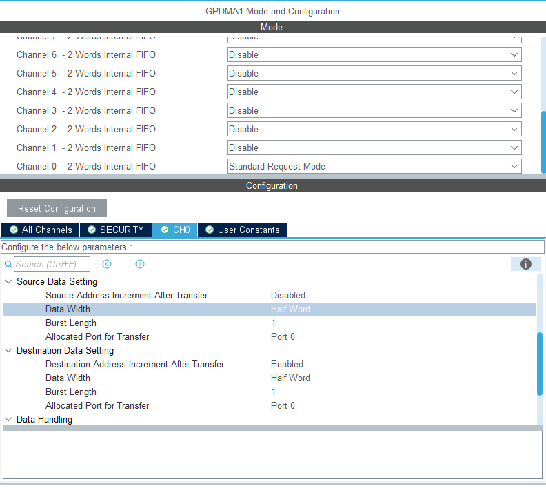
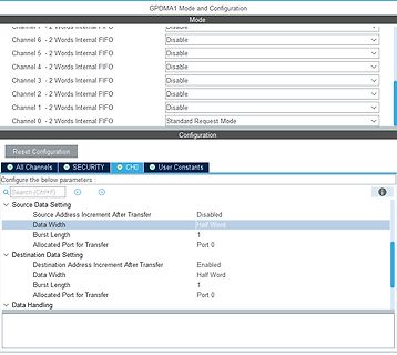
Konfigurationsmenü eines GPDMA1 Moduls
Configure the below parameters : Search (Ctrl+F) Source Data Setting Source Address Increment After Transfer Disabled Data Width Half Word Burst Length 1 Allocated Port for Transfer Port 0 Destination Data Setting Destination Address Increment After Transfer Enabled Data Width Half Word Burst Length 1 Allocated Port for Transfer Port 0 Data Handling
in „STM32U575 und ILI9341 SPI DMA Problem“ · Mikrocontroller und Digitale Elektronik · · Screenshots
-
PDF
24lc16.pdf
been defined: an overwrite does occur it will replace data in a first in first out fashion. Data transfer may be initiated only when the bus is not busy. During data transfer, the data line must remain 3.5 Acknowledge stable whenever the clock line is HIGH. Changes Each receiving device, when addressed
in „Tipsend2 Pollin“ · Mikrocontroller und Digitale Elektronik ·
-
 Bild
Bild
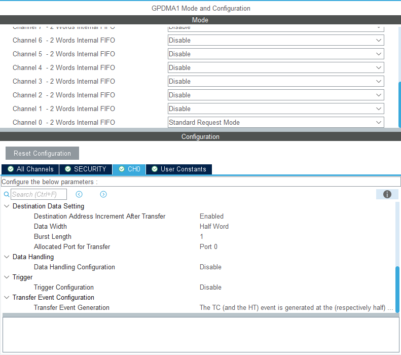
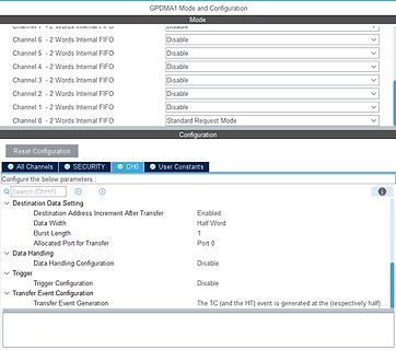
Software-Konfigurationseinstellungen für GPDMA1 Mode
below parameters : Search (Ctrl+F) Destination Data Setting Destination Address Increment After Transfer Enabled Data Width Half Word Burst Length 1 Allocated Port for Transfer Port 0 Data Handling Data Handling Configuration Disable Trigger Trigger Configuration Disable Transfer Event Configuration Transfer Event Generation The TC (and the HT) event is generated at the (respectively half) ...
in „STM32U575 und ILI9341 SPI DMA Problem“ · Mikrocontroller und Digitale Elektronik · · Screenshots
-
PDF
STM32_general-purpose_timer_cookbook_en.DM00236305.pdf
timer DMA burst feature, TIMx_DCR, is used to configure the number of beats during a single burst transfer. It is also used to identify the target timer register or the source of the first data transfer during a burst transfer. The DBL [4:0] control bit-field sets the number of beats during one burst transfer
in „STM32 Timer Cookbook PWM - Beispiel 6.2“ · Mikrocontroller und Digitale Elektronik ·
-
PDF
Applnote.pdf
timer DMA burst feature, TIMx_DCR, is used to configure the number of beats during a single burst transfer. It is also used to identify the target timer register or the source of the first data transfer during a burst transfer. The DBL [4:0] control bit-field sets the number of beats during one burst transfer
in „PWM Signalerzeugung“ · Mikrocontroller und Digitale Elektronik ·
-
Datei
USI_TWI_Master.asm
Pull SCL LOW. ld temp5, X+ out USIDR, temp5 // Setup data. mov temp6, temp3 rcall USI_TWI_Master_Transfer // Send 8 bits on bus. /* Clock and verify (N)ACK from slave */ cbi DDR_USI, PIN_USI_SDA // Enable SDA as input. mov temp6, temp4 rcall USI_TWI_Master_Transfer andi temp6, 1<<TWI_NACK_BIT breq USI_SUCCESS
in „C->Asm (TWI) Fehlersuche“ · Mikrocontroller und Digitale Elektronik ·
-
Datei
dogxl_hardware.c
TX DMA //enable trigger source interrupt IFS0bits.SPI1IF = 1; //make sure, flag is set for first transfer SPI1STATbits.SPIROV = 0; //Clear Receive Buffer overflow bit //reset bits DMAINT0bits.DONEIF = 0; DMAINT1bits.DONEIF = 0; //kick off data transfer by generating a request DMACH0bits.CHREQ = 1; DMACH1bits.CHREQ
in „PIC24FJ128GA306 und DMA“ · Mikrocontroller und Digitale Elektronik ·
-
Datei
rc522.c
include "rc522.h" void rc522_write( uint8_t addr, uint8_t val) { SELECT_PORT &= ~(1<<SELECT_PIN); spi_transfer( (addr<<1) & 0x7E ); spi_transfer( val ); SELECT_PORT |= (1<<SELECT_PIN); } uint8_t rc522_read( uint8_t addr ) { SELECT_PORT &= ~(1<<SELECT_PIN); spi_transfer( ( ( addr<<1 ) & 0x7E ) | 0x80 ); uint8_t ret = spi_transfer( 0x00 ); SELECT_PORT |= (1<<SELECT_PIN); return ret; } void rc522_init() { SELECT_DDR |= (1<<SELECT_PIN); SELECT_PORT |= (1<<SELECT_PIN); spi_init(); rc522_reset(); } void rc522_reset() { rc522_write
in „Atmega32 und MFRC522 per SPI“ · Mikrocontroller und Digitale Elektronik ·
-
PDF
DS3231.pdf
the most signifi- ate the STOP condition. cant bit (MSB) first. Figures 3 and 4 detail how data transfer is accomplished Data transfer from a slave transmitter to a master on the I C bus. Depending upon the state of the R/W bit, receiver. The first byte (the slave address) is transmit- two types of data transfer are possible: ted by the master. The slave then returns an acknowl- edge bit. Next follows a number of data bytes transmit- Data transfer from a master transmitter to a slave receiver. The first byte
in „18650 Zelle zu 5V“ · Analoge Elektronik und Schaltungstechnik ·
-
PDF
DS3231.pdf
the most signifi- ate the STOP condition. cant bit (MSB) first. Figures 3 and 4 detail how data transfer is accomplished Data transfer from a slave transmitter to a master on the I C bus. Depending upon the state of the R/W bit, receiver. The first byte (the slave address) is transmit- two types of data transfer are possible: ted by the master. The slave then returns an acknowl- edge bit. Next follows a number of data bytes transmit- Data transfer from a master transmitter to a slave receiver. The first byte
in „DS3231 vs PCF8573, hilfe gesucht !“ · Mikrocontroller und Digitale Elektronik ·
-
PDF
DS3231_S_SN_Crystal.pdf
the most signifi- ate the STOP condition. cant bit (MSB) first. Figures 3 and 4 detail how data transfer is accomplished Data transfer from a slave transmitter to a master on the I C bus. Depending upon the state of the R/W bit, receiver. The first byte (the slave address) is transmit- two types of data transfer are possible: ted by the master. The slave then returns an acknowl- edge bit. Next follows a number of data bytes transmit- Data transfer from a master transmitter to a slave receiver. The first byte
in „(empfindlicher) GPS Modul gesucht“ · Mikrocontroller und Digitale Elektronik ·