DIMENSIONS Millimeters Inches H2 A Min. Max. Min. Max. C A 4.40 4.60 0.173 0.181 C 1.23 1.32 0.048 0.051 L5 Ø I L7 D 2.40 2.72 0.094 0.107 E 0.49 0.70 0.019 0.027 L6 F 0.61 0.88 0.024 0.034 L2 F1 1.14 1.70 0.044 0.066 G 4.95 5.15 0.194 0.202 D L9 H2 10.00 10.40 0.393 0.409 L2 16.40 typ. 0.645 typ. F1 L4 L4 13.00 14.00 0.511 0.551 L5 2.65 2.95 0.104 0.116 M L6 15.25 15.75 0.600 0.620 F E L7 6.20 6.60 0.244 0.259 G L9 3.50 3.93 0.137 0.154 M 2.6 typ. 0.102 typ. Diam. I 3.75 3.85 0.147 0.151 Marking: type number Cooling method: by
~/media/marketing/de/service/ersatzteil/velux-fensterkomponenten-innen.png?h=280&la=de-DE&mw=768&w=620 Und die Abdichtungen sind halt so ungefähr gemacht: http://ecx.images-amazon.com/images/I/41WbSVnoUzL.jpg Danke sehr!
PB3 G C3 (SS)PB4 5 MISO 1 2 VCC 6 3 4 2 2 100n (MOSI)PB5 SCK MOSI 2 D 4 D (MISO)PB6 7 RST 5 6 GND D L D L Lowest Level 8 1 1 (SCK)PB7 AVR-ISP-6 DIL40 RST B 22 GND B (SCL)PC0 R9 (SDA)PC1 23 150 24 (TCK)PC2 (TMS)PC3 25 via 150R to cathodes 26 2 2 (TDO)PC4 3 D 5 D (TDI)PC527 D L D L Highest Level 28 1 1
RIPPLE CURRENT Set the nominal inductor ripple current (ΔL-PP) by solving for the appropriate inductor (L1): Buck (VIN-V O)xD L1= ü xf i L-PP SW (44) Boost and Buck-boost 30 VIND L1= ü i x f L-PP SW (45) To set the worst case inductor ripple current, use VIN-MAXand D MIN when solving for L1. The minimum
sollte das machbar sein, vor allem da der geschaltete R ja relativ niederohmig sein kann und damit L/C nicht so dominant werden können... PS - ich würd das Relais nie so schalten daß es einen offenen Signalpfad im Moment des Umschaltens gibt... Aus der Sicht des OPVs sind die 5ms Umschaltzeit eine
bischen besser jonglieren, die 0,1% sollten eigentlich passen... Im Schaltplan ist bei dem von L2/L13 entkoppelten IC zwar die Pinnummer 4&8 sichtbar, es ist aber nicht ersichtlich, welches IC das nun ist. Das selbe ist auch bei IC4 der Fall (reine Schaltplankosmetik) Du kannst die L2/L13 auch
D S D SF Transistor / 5 V Mosfet / 12 V 6,3A V 3K9 R150 3 F1 2 P A IRFP460 G G M s C BC338-25 0 0 L L ( 1 1 N 5 R120 SFH620A-3 2 F 4 F D 1 5 D S D S P 2 4 GND_1 GND_2
Hallo, Ich habe einen Vaillantheizkessel, Solaranlage und auromatic 620 Steuerung, läuft ja auch alles über eBus. Vielleicht klappt das Auslesen ja auch mit der Software von RESOL.de, die nennen die Schnittstelle Vbus, scheint aber das Gleiche zu sein. Würde mich
etc/sysconfig/rpcbind: [pre]# Optional arguments passed to rpcbind. See rpcbind(8) RPCBIND_ARGS="-l"[/pre] Firewalls sind abgeschossen bzw. deaktiviert. SeLinux habe ich ruhig gestellt in /etc/selinux/config: [pre]# This file controls the state of SELinux on the system. # SELINUX= can take one
send_cmd(0xCA83); // enable FIFO RFM12_PORT &= ~(1<<RFM12_SCK); // CLK auf L RFM12_PORT &= ~(1<<RFM12_SDI); // DATA auf L for (i=0; i<len; i++) { RFM12_PORT &= ~(1<<RFM12_CS); // CS auf L asm("nop"); asm("nop");
statusword = 0; unsigned char i = 0; RFM12_PORT &= ~(1<<RFM12_SCK); // CLK auf L RFM12_PORT &= ~(1<<RFM12_SDI); // DATA auf L RFM12_PORT &= ~(1<<RFM12_CS); // CS auf L for (i = 0; i < 16; i++) { statusword = (statusword << 1);
calculationsfortheshorted-linefail-safecircuitforsomeinsightonhowthevalues can be modified for a particular design. 8 SLLA036 5 V Open Idle Short u.l. A, dB R3 R1 R1 = 2500 R3 = 110 Y Y Y 5.6 –0.5 a) R2 R2 R2 = 120 R3 27000 R1 = R1 R3 = 1000 Y Y Y 1.5 –1 R2 = 120 5 V R1 Open Idle Short u.l. A, dB b) R2 R2 R1 = 620 R2 = 120 Y Y N 20.5 0 R1 5 V R1 Open
--- uint16_t rfm12_send_cmd(uint16_t command) { uint8_t i; RFM12_PORT &= ~(1<<RFM12_CS); // CS auf L for (i=0; i<16; i++) { if (command & 0x8000) // MSB testen und senden { RFM12_PORT |= (1<<RFM12_SDI); // DATA auf H } else { RFM12_PORT &= ~(1<<RFM12_SDI); // DATA auf L } RFM12_PORT |= (1<<RFM12_SCK
oder geregelten Kühlung mit einem oder mehreren Lüftern im Verbund e i o - Elektrischer Anschluss l : l : e U o n n n n t g s Lüfter Kunde s g s g b u i x (+) Power UB h L d h H d h a l k UB Signaldaten T U B T US B T sp Z Is +UBS Typ V DC mA V DC mA V DC mA Ausgang 250 ≤0,4 ≤2 30 0 ≤30 2 Iink US 400
oder geregelten Kühlung mit einem oder mehreren Lüftern im Verbund e i o - Elektrischer Anschluss l : l : e U o n n n n t g s Lüfter Kunde s g s g b u i x (+) Power UB h L d h H d h a l k UB Signaldaten T U B T US B T sp Z Is +UBS Typ V DC mA V DC mA V DC mA Ausgang 250 ≤0,4 ≤2 30 0 ≤30 2 Iink US 400
4/π times that of the square wave as shown by the waves. For example, the 350Hz, 440Hz, 480Hz, and 620Hz Fourier series. The bandpass filter will also filter out any DC telephone supervisory tones transmitted over fiber-optics component of the square wave input as shown in Figure 1B. may appear at curb-side
with Grundfos pumps. M h o d s w 2-pole 4-pole The motors meet international design standards, and l s r Type Efficiency Type Efficiency within each motor type we offer a number of different designation class designation class 1-2-3 1-2-3 variants. If you do not find the specific motor variant 3 0.25
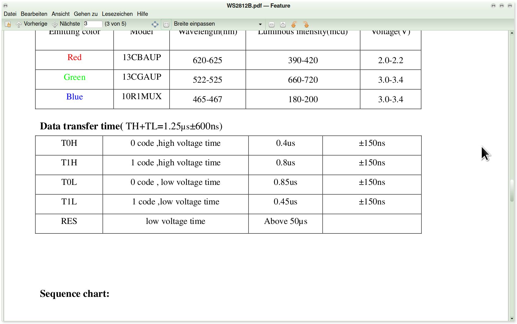
WS2812B.pdf - Feature
Red 13CBAUP 620-625 390-420 2.0-2.2
Green 13CGAUP 522-525 660-720 3.0-3.4
Blue 10R1MUX 465-467 180-200 3.0-3.4
Data transfer time( TH+TL=1.25µs±600ns)
T0H 0 code, high voltage time 0.4us ±150ns
T1H 1 code, high voltage time 0.8us ±150ns
T0L 0 code, low voltage time 0.85us ±150ns
T1L 1 code, low voltage time 0.45us ±150ns
RES low voltage time Above 50µs
Sequence chart:
Johann L. schrieb im Beitrag #7959037: > In anderen Sprachen fügt man einfach eine neue Funktion hinzu, zum > Beispiel zum Zeichen eines Kreises. In den anderen Sprachen ist exakt definiert, wie eine Funktion
Johann L. schrieb im Beitrag #7959071: > um die Hirnwindungen > forthkompatibel zu bekommen Ja! Das ist ein Projekt. Glaube auch nicht, dass das es jeder bis in die Komfortzone schafft. Vorbildung in
1 2 3 4 A A 3V3 L1L D3D VPP U3U 1.5inch RGB OLED P1 VCC PIL101 PIL102PID301 PID302 7PIP107 4.7uH SS14 24C 128(RGB) x 128 Pixels 5PIP105 GND U2U 22uF/50V 4PIPCS4 I2101 5 1 2PIP102 I22uF PIU2IN SW PIU201 I1 GND D D 1PIP101 PIU2EN NC PIU206 620K 1% G M D D F O OD G B Header 7 PIU2GND FBPIU203 I2 N V V V V N D D D D D D D D E R B B C D R I G G N V V V N N IR7R J1J VCC SX1308 30K 1% GND 0UP045U67801P11 1 1 1 1 1 1 1 2 2 2 2 2 2 2 2 2 2 3 1PIJ101
number are not less than 512 points, high speed mode not less than1024 points. l Send data at speeds of 800Kbps. l The color of the light were highly consistent, cost-effective.. Applications l Full-color module, Full color soft lights a lamp strip. l LED decorative lighting, Indoor
number are not less than 512 points, high speed mode not less than1024 points. l Send data at speeds of 800Kbps. l The color of the light were highly consistent, cost-effective.. Applications l Full-color module, Full color soft lights a lamp strip. l LED decorative lighting, Indoor
number are not less than 512 points, high speed mode not less than1024 points. l Send data at speeds of 800Kbps. l The color of the light were highly consistent, cost-effective.. Applications l Full-color module, Full color soft lights a lamp strip. l LED decorative lighting, Indoor
number are not less than 512 points, high speed mode not less than1024 points. l Send data at speeds of 800Kbps. l The color of the light were highly consistent, cost-effective.. Applications l Full-color module, Full color soft lights a lamp strip. l LED decorative lighting, Indoor
F2 1.14 1.70 0.044 0.067 G 4.95 5.15 0.194 0.203 G1 2.4 2.7 0.094 0.106 H2 10.0 10.40 0.393 0.409 L2 16.4 0.645 L4 13.0 14.0 0.511 0.551 L5 2.65 2.95 0.104 0.116 L6 15.25 15.75 0.600 0.620 L7 6.2 6.6 0.244 0.260 L9 3.5 3.93 0.137 0.154 DIA. 3.75 3.85 0.147 0.151 E A C D D L2 1 F 1 G 2 G H Dia. F 2 L5 F L9 L7 L6 L4 P011C 7/8 PB137 Information furnished is believed to be accurate and reliable. However, STMicroelectronics assumes no responsibility forthe consequences of use of such information nor
F2 1.14 1.70 0.044 0.067 G 4.95 5.15 0.194 0.203 G1 2.4 2.7 0.094 0.106 H2 10.0 10.40 0.393 0.409 L2 16.4 0.645 L4 13.0 14.0 0.511 0.551 L5 2.65 2.95 0.104 0.116 L6 15.25 15.75 0.600 0.620 L7 6.2 6.6 0.244 0.260 L9 3.5 3.93 0.137 0.154 DIA. 3.75 3.85 0.147 0.151 E A C D D L2 1 F 1 G 2 G H Dia. F 2 L5 F L9 L7 L6 L4 P011C 7/8 BUZ11 Information furnished is believedtobeaccurateand reliable.However, STMicroelectronics assumes no responsibilityforthe consequences of use of such information nor for any
F2 1.14 1.70 0.044 0.067 G 4.95 5.15 0.194 0.203 G1 2.4 2.7 0.094 0.106 H2 10.0 10.40 0.393 0.409 L2 16.4 0.645 L4 13.0 14.0 0.511 0.551 L5 2.65 2.95 0.104 0.116 L6 15.25 15.75 0.600 0.620 L7 6.2 6.6 0.244 0.260 L9 3.5 3.93 0.137 0.154 DIA. 3.75 3.85 0.147 0.151 E A C D D L2 1 F 1 G 2 G H Dia. F 2 L5 F L9 L7 L6 L4 P011C 7/8 PB137 Information furnished is believed to be accurate and reliable. However, STMicroelectronics assumes no responsibility forthe consequences of use of such information nor
periods may affect reliability. Truth table CE1 CE2 WE OE Data Mode H X X X High Z Standby (SB, SB1) X L X X High Z Standby (I , I ) SB SB1 L H H H High Z Output disableCC) L H H L D OUT Read (CC) L H L X D Write ( ) IN ICC Key: X = don’t care, L = low, H = high May 2015 v 2.0 Alliance Memory Inc P. 2 of
Transportation Packing and Materials Barcodelabel Barcodelabel 02- P 1-:1 n i2B: p SR 676 D BinB Te2L0C CR RT T EMY Y T PSE M 2 a 2460C l2X 8 LtiTO 2 3 d tia R:R1 Q - Mu l e Ad 077CKRA P-1+ L PA UO: V E l t (G)GR LE l,see).e b c dno(RH 4 s bar d iy . to s 98 : 14 u m i R H O pctr 0 219 D)D/C vi h e /
########################### 'Settings for RFM12 'word for SPI Tx Dim Spi_tx_wrd As Word Dim Spi_tx_l As Byte At Spi_tx_wrd Overlay Dim Spi_tx_h As Byte At Spi_tx_wrd + 1 Overlay 'word for SPI Rx Dim Spi_rx_wrd As Word Dim Spi_rx_l As Byte At Spi_rx_wrd Overlay Dim Spi_rx_h As Byte At Spi_rx_wrd + 1
impedance and very low OFF leakage current. Control of analog signals up to the complete supply voltage L SUFFIX range can be achieved. CERAMIC CASE 620 Triple Diode Protection on Control Inputs Switch Function is Break Before Make Supply Voltage Range = 3.0 Vdc to 18 Vdc Analog Voltage Range (V – V ) =
impedance and very low OFF leakage current. Control of analog signals up to the complete supply voltage L SUFFIX range can be achieved. CERAMIC CASE 620 Triple Diode Protection on Control Inputs Switch Function is Break Before Make Supply Voltage Range = 3.0 Vdc to 18 Vdc Analog Voltage Range (V – V ) =
SwitcherCAD is also available. SwitcherCAD is a trademark of Linear Technology Corporation. O U TY I P CA L PP IC I L AT Boost Converter (5V to 12V) MaximumOutput Power* 5V L1** L2 OUTPUT 100 *ROUGH GUIDE ONLY. BUCK MODE 50 H 10 H FILTER LT1170 SPECIAL TOPOLOGIES DELIVER C3 80 MORE POWER. D1 100 F **DIVIDE
2.0 2.5 3.5 5.0 5.0 7.5 7.5 P ±0.5 ød 0.5 0.5 0.6 0.6 0.6 0.8 0.8 4 β 0.5 0.5 0.5 0.5 0.5 0.5 0.5 L +α max. 15 min. min. øD +β α 1.0 1.5 max. Working Voltage; Dimensions: øD x L (mm); Ripple Current: mA/RMS @ 120Hz, 105°C Value 6.3 10 16 25 35 50 63 100 (µF) øD x L mA øD x L mA øD x L mA øD x L mA øD x L mA øD x L mA øD x L mA øD x L mA 0.1 5 x 11 1.3 5 x 11 2.6 0.22 5 x 11 2.9 5 x 11 5.8 0.33 5 x 11 4.4 5 x 11 8.8 0.47 5 x 11 7 5 x 11 12 1 5 x 11 13 5 x 11 22 2.2 5 x 11 29 5 x 11 33 3.3 5 x 11 35 5
Martin L. schrieb im Beitrag #7025892: > Beim Antwortsatz bitte dieses Mal nicht den Satzpunkt vergessen. Punkt, Satz und Sieg.
dann auch keinen Stromfluss geben. Erst bei T > 0 wächst auch die Aufenthaltswahrscheinlichkeit im L-Band und damit wird der Halbleiterkristall el. leitend.
erstelle und darin messwerte abspeichere erkennt er mir kein enter zb.: 2010-01-10 12:32:11;14,532;l/s;29328398.2938;m3<ENTER> 2010-01-10 12:32:12;14,532;l/s;29328398.2938;m3<ENTER> 2010-01-10 12:32:13;14,532;l/s;29328398.2938;m3<ENTER> 2010-01-10 12:32:14;14,532;l/s;29328398.2938;m3<ENTER> 2010
ich rufe im Main folgenden Code auf: [c] int main(void) { UC ucBuffer[512] = {'H','a','l','l','l','o',' ','W','e','l','t'}; UC ucRetSD = 0; ucRetSD = sd_raw_init(); //SD Karte starten if(ucRetSD) { UART_send_String_while("\nSD init OK\n"); } else
angesiedelt. Ihr obiger Vorschlag wirkt (i.d.Z.) eher "vorsintflutlich", man setzt hier spezielle L.E.D. und Mikroprozessoren ein. Ihr Gedankengang ist aber weitgehend richtig, wie sie dem beigefügten Bildmaterial entnehmen können. Liebe Grüße Ihr Max Meierhofmann
nicht): Ebenfalls suboptimal ist die Verteilung der 3V3 (scheinbar der Digitalteil da vor dem L abgegriffen) unter dem Xmega. Mach ein 3V3-Polygon/Shape unter dem Xmega - damit sinkt der induktive Anteil erheblich, was hier erstrebenswert ist. Den Abgriff am L kann man auch wesentlich breiter gestalten
Moin! Afair wurde ein L Typ genommen, also ein 78L08, somit sollte das IC4 unter dem Port B sein. Grüsse Thomas
InputErrorVoltagevs.OutputVoltageWithin300mVofEither SupplyRailforVariousResistiveLoads;V =±5S 10M 1k ) H ) V S ±15V / / R L 100kΩ V ( 1M ( 100 N VS= 0V, +5V E I I G N P V S ±15V E O R L 10kΩ G O A - VS= 0V, +5V L N O P100k V 10 O V = ±15V T S P R L 600Ω I V = 0V, +5V 1 1 S 3 3 0 0 10k 0 1 0 –60 –40 –20 0 20 40 60 80 100 120
co ± 5 date i e e 4 24 6H o C TOI SE t <4w lt p).i ct r 23 ˚C w ih oortrti i e e MPT O ts ahatalen l a tf at e. tral FlFloo ortrti O m on qesitlb e ow ,i:r ad edu iden l4 FF l o 4d:e,iore ode be l ti hen p r c e is L evevel5l5a6 ebflow arc see o%n w a ke ld at ure eL L evevel l d pe ere ee b ti e ore

 Bild
 Bild