V = 440 V DC or V AC, V = 400 V DC or V AC, T = 120 °C (typ.), R = ±25 % max R ref R B750 123 245 4.0 4 25 13 X X B59750B0120A070 B770 64 127 2.8 3.0 70 45 X X B59770B0120A070 C751 87 173 4.0 3.5 50 26 X X B59751C0120A070 C752 69 137 4.0 3.5 80 42 X X B59752C0120A070 C753 56 112 4.0 3.0 120 63 X X
view Bottom view 1 2 3 4 5 6 7 7 6 5 4 3 2 1 A A B B C C D D E E F F G G Table 1-2. BGA - pinout 1 2 3 4 5 6 7 A GND PB4 PB2 GND VCC PA2 GND B PB6 PB5 PB3 PB0 PA0 PA3 PA5 C VCC RESET PB7 PB1 PA1 PA6 AREF D GND XTAL2 PD0 GND
puts. than 1 OmA. Input-signalinterfacesthatswingthe allowable 0.5V above Voo or below Vss should 4) Paralleling gates isrecommended onlywhenthe be current-limited to1 OmAor less. gates are within the same IC package. Whenever the possibility of exceeding 1OmAof input current exists, a resistor in
registers. organized as below: Register Function 0 Software version 1 Compass Bearing as a byte, i.e. 0-255 for a full circle 2,3 Compass Bearing as a word, i.e. 0-3599 for a full circle, representing 0-359.9 degrees. 4 Pitch angle - signed byte giving angle in degrees from the horizontal plane 5 Roll
, 4 identical cards are used. Identical means that the same devices are used, and that the I C 2 load in the bus to 400 pF. In applications where a higher capacitive load is required, 2 types of devices
precursor data and combining physics-of-failure models to predict the used in automotive circuits (e.g., the protection of micromotors remaining useful life (RUL) of PPTC resettable fuses. in window lifts, seats, and door locks), computers (e.g., the protection of the circuits in hard disk drives, interface
2017 Microchip Technology Inc. Datasheet Preliminary DS40001893B-page 16 8-bit AVR Microcontroller 4.4 24-pin QFN I D U T S E 1 0 5 4 3 2 A A C C C C P P P P P P 2 2 2 2 2 1 PA2 1 18 PC1 EXTCLK/PA3 2 17 PC0 GND 3 16 PB0 VDD 4 15 PB1 PA4 5 14 PB2/TOSC2 PA5 6 13 PB3/TOSC1 7 8 9 0 2 1 1 1 A A B B B B P
2020 Microchip Technology Inc.Preliminary Datasheet DS40002183A-page 16 AVR128DA28/32/48/64 Pinout 2.4 64-Pin VQFN and TQFP ) L T C E X E ( I ( 2 1 0 7 6 5 4 D D 3 2 1 0 D 6 5 A A A G G G G N D G G G G P F F P P P P P P P G V P P P P U P P 6 6 6 6 6 5 5 5 5 5 5 5 5 5 5 4 PA3 1 48 PF4 PA4 2 47 PF3 PA5
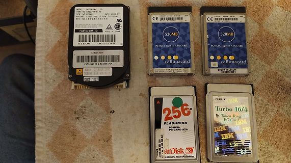
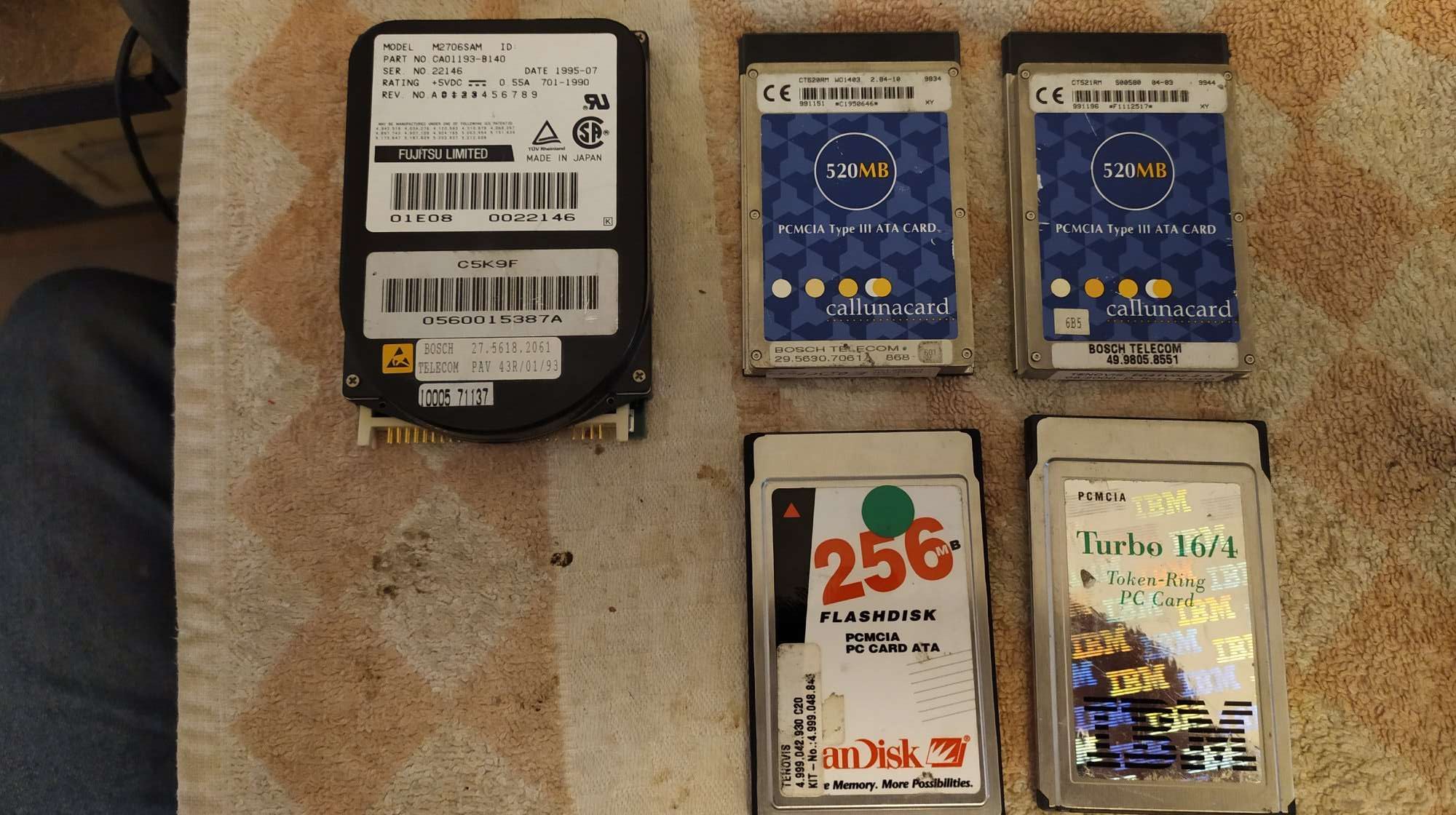
MODEL M2706SAM ID
PART NO CA01193-B140
SER NO 22148
RATING +5VDC 0.55A 701-1990
REV NO A 0 1 2 3 4 5 6 7 8 9
FUJITSU LIMITED MADE IN JAPAN
01E08 0022146
520MB PCMCIA Type III ATA CARD
callunacard
BOSCH TELECOM
29.5630.7051
nach passen die kannmangültigeWertefürdieWiderstän- resultierenden restlichen beiden Wider- de R1, R4, R8 und R9 berechnen: stände nicht in die E12-Reihe. Diese setzt 10·R8·R9<11·(R1+R4)·(R8+R9) man des halb am einfachsten durch eine 10·(R1+R4)·(R8+R9)<11·R8·R9 Reihen- oder Parallelschaltung von je zwei
habe ich angesetzt und diesen Zweig von der Ausgabe getrennt und verwende nun den internen DAC vom SAM4E16E und schleuse das Signal so ein, funktioniert! Nun habe ich bis jetzt meine EKG Signale selbst mit Excel designt, was jedoch ziemlich umständlich ist (siehe Bild_1). Die DAC Werte werden dann
FREE PLATED (8 mm TAPE), (8 mm TAPE), (EXAMPLE) STANDARD GREEN 15K/BOX = MOQ 10K/BOX = MOQ GSOT05C- E 3 -08 GSOT05C-E3-08 GSOT05C- G 3 -08 GSOT05C-G3-08 GSOT05C- H E 3 -08 GSOT05C-HE3-08 GSOT05C- H G 3 -08 GSOT05C-HG3-08 GSOT05C- E 3 -18 GSOT05C-E3-18 GSOT05C- G 3 -18 GSOT05C-G3-18 GSOT05C- H E 3 -18
DC *V electrical Max. switching current 6 A Constant current Ith2 6 A Constant current Ith2at the same time over 2 contacts 4,2 A Constant current Ith2at the same time over 3 contacts 3,4 A Switching capacity NO-contact/NC-contact AC-15 230/240 V le=4/1,2 A NO-contact/NC-contact DC-13 24 V le=2/1,2 A
A A A V S CS index area 2 2 2 2 2 1 LED0 1 18 RESET LED1 2 17 LED15 LED2 3 16 LED14 PCA9532BS LED3 4 15 LED13 LED4 5 14 LED12 LED5 6 13 LED11 7 8 9 1 1 1 6 7 S 8 9 1 E DE V E DE D 002aae520 L L L L L Transparent top view Fig 4. Pin configuration for HVQFN24 PCA9532 All information provided in this document
Product Series UDP3305S series programmable DC power supply includes two models: UDP3305S and UDP3305S-E. The output ranges are shown in the table below: Maximum output current Model Maximum output voltage CH1: 33V CH1: 5.2A UDP3305S CH2: 33V CH2: 5.2A CH3: 6.2V CH3: 3.2A UDP3305S-E CH4: 2A CH4: 5V UDP3305S
wiki: The eZ80 (like the Z380) is binary compatible with the Z80 and Z180, but almost three times as fast as the original Z80 chip at the same clock frequency.
der dort benannten Bugs > des Emulators)? Was hast du erwartet? Genau das ist ja die Domäne der "4-Bitter": Einsatz in Produkten, die keine große Rechenleistung erfordern und in >10e6-Auflagen produziert werden. Soweit ich weiß wurden (werden) zum Beispiel als Nachfolger der Magnetstreifen-Varianten
t e e h s PS817-070WS-C-IPS-46 a EVE4 IPS 7.0’’ LCD DATASHEET t REV.1.0 a 2024-01-04 D ITEM CONTENTS UNIT LCD Type TFT / Transmissive / Normally Black / y Size 7.0 Inch Viewing Direction Normally Black O'C
nicht mehr zum Debuggen nutze, evtl. vor 20 jahren mal) reicht mir putty. STM32: STM32CubeIDE AtSAM: Atmel Studio (oder heißt das nun Microchip Studio) usw. immer die mitgelieferte IDE nutzen. Also ich will programmieren und mich nicht mit irgend einem Aufhübschen von irgendwelchen IDEs beschäftigen
steinzeitlichen linearen EVA-Architektur und berücksichtigen nicht, das es einen Feedback-Pfad zwischen V und E geben könnte.
Current vs. Fig 10. Threshold Voltage vs. Temperature Case Temperature 10 ) C 1 D = 0.50 J t ( 0.20 e 0.10 n R1 R2 R3 R4 Ri (°C/W) τι (sec) o 0.1 0.05 R1 R2 R3 R4 s ττJ ττ 0.003454 13.68748 e 0.02 τ1 τ τ 0.17246 7.21E-05 l 1 2τ2 3τ3 ττ4 a 0.01 0.786312 0.001227 r Ci= τi/Ri 1.368218 0.007178 h 0.01 Ci
1.1.0 2 S S 8 0 Typical Performance Characteristics 5 0 — 0.5 1000 N V = 1V P CE T B = 3.0mA N N 0.4 E R I = 2.5mA N R B A 100 p C G t R 0.3 B = 2.0mA T a O E x C R a E B = 1.5mA U l L 0.2 C O C 10 S , B = 1.0mA , l A F c IC 0.1 h o B = 0.5mA n 1 T 0 0.4 0.8 1.2 1.6 2.0 0.1 1 10 100 1000 r a n VCEV]
der (erwarteten Fehlermeldung) auf der Konsole: [code] root:/tmp/r4# bossac -d --port=ttyACM0 -U -e -w blink_r4.bin Set binary mode Send auto-baud Set binary mode No device found on ttyACM0 [/code] lsusb sagt mir: [code] Bus 002 Device 003: ID 05e3:0607 Genesys
billigen Nachbauten auch gerne mal. Dort war’s aber kein Problem, den via ISP draufzutun – wie es beim R4 aussieht, weiß ich allerdings nicht im Detail.
operational. To assure a noise margin, the MOS-FET’s should have a minimum threshold voltage V of e.g. 0.4V and VDD1 must stay below this value. The isolation feature can also be applied if no level shifting is required, VDD1 and VDD2 may have the same value, e.g. both 3.3V or both 5V. 11 Philips Semiconductors
EXPONENT 0 + / - LOCATION 1 IEEE-488 INTERFACE 1 1 O O1 1 01 1 O S A T T L L S R P D C E A2A1 A3 A4 DIGITAL I/O EXTERNAL TRIGGER SENSING INPUT LOCAL OUTPUT REMOTE LINE RATING FUSE 50-60 Hz AC, 80 VA MAX LINE VOLTAGE SELECTED 90-110V 180-220V 105-125V 210-250V SLOWBLOW 3/4A 90-125V MADE IN
-Taping specification for axial capacitors Description Symbol Dimensions (mm) Capacitor diameter D 4,5÷ 19,5 Capacitor length L 10,5÷ 32,0 Component pitch A* Seetable I Reel core diameter E 60 Arbor core diameter M 16 Reel diameter ø 340+5 Marking F Seetable II Tape width H 6±0,5 Body location (lateral
transducer system. E Earthing connection generator print >> earthing point on bottom plate. HF output T780 – T890 G F E C D Illustration 14.4.2. Detailed view HF output C HF (+) output (plug ocntact 6.3 mm). D Earthing point
-18 GPIO Connector Pin-out (J13) 21 Data Sheet Rev1.1 V A R - 6 U C U S T O M B O A R DD A T A S H E E R E V 1 . 1 2.4 User Interfaces 2.4.1 LED Indications 2.4.1.1 Power-On LED (D24) Led D24 indicates that the SoM 3.3V power supply is ON and supplies the voltage to the SoM. 2.4.1.2 Peripheral 3.3V
Current control unit TIC 226 detector ö = f (V3) C 1 R 100 mF/ 3 8 Supply 25 V voltage 180W limiting 4 GND – Reference Full wave load + voltage 1 current detector Voltage Soft start monitoring 2 3 R10 P1 68 kW Set point C 5 Soft start 50 kW 4.7mF/ 25 V C 3 C4 R7 10 nF 100 nF 220 kW N Figure 2. Block diagram
o H m r s v r 6 O t 1 + t d 1 W o W K o R M t k 5 e 1 S R 8. Y v u 2 v i B O t w t g o O l e C5 P W 1 l a 1 F r m Fm 0 D v n . 5 5 t n n p 5 0 0 4 e ot a o – C ku n k M c 1 0d pe R 70 4 R 1oa m 4 1 t L c W n 4 / a s ul ( l W R m h r f v i 3 F k a 5 e
is an internal device dielectric breakdown rating. For this test, pins 1 and 2 are common, and pins 4, 5 and 6 are common. www.onsemi.com 4 MOC3051M, MOC3052M, MOC3053M TYPICAL CHARACTERISTICS 1.7 400 ) V A ( 1.6 ( 300 E T A 1.5 E 200 T R O 1.4 R 100 V U D C R 1.3 T 0 A TA= −40°C A W 1.2 S −100 O TA=
Versions VO = 2 V TA= 25°C High-Bias Versions No Load A A 1000 µ 1000 µ – – t Medium-Bias Versions n e e Medium-Bias Versions u u C 100 C 100 l l p p u Low-Bias Versions u – – D D Low-Bias Versions ID 10 ID 10 0 0 0 2 4 6 8 10 12 14 16 18 20 0 10 20 30 40 50 60 70 80 VDD – Supply Voltage – V TA– Free-Air
Ich wäre bei c‘t Beiträgen, die in einem Heft mit Laufzeit über den 1.4. stehen, etwas entspannter. 😉
aber auch nicht sein, schrieb ich ja auch oben: kann man eh nicht sehen oder nicht lesen. Aber "3/4 fertig" ist besser als "sst sst - Wo war ich nochmal?" Ja, ginge auch mit 4 LEDs...
-227 TO-264 PLUS247 Height=5.3mm Height=8.92mm Height=4.8mm Height=4.8mm The above accentuates the compact and low profile nature of the device. Compared to a conventional high power package such as the SOT-227, the IXYS SMPD features ¼ the weight and 1/3
the hole at a rapid retract rate. The drill then moves to point B, and the cycle is repeated. The same sequence is followed for holes C, D and E. After the completion of the last hole the drilling head may be instructed to return to the original starting point or to another parking position and automatically
are connected to a dedicated digital inputpin on the LPC17XX. Multiple keys can be pressed at the same time (e.g. up and right). Inputpins are active low when a key is pressed. The inputpins are hardware debounced. LandTiger V2.0 User Manual 24 Figuur 19 Joystick 5-Way Switch Tabel 21 Joystick 5-way
3 6 7 M M M M M R18 470R W W W W W 2 3 P P P P P VDD BACKUP SELECT 2 J16 1 1 J17 R20 470R 3.63V6 . E 1 4 3.00V +- 0.2% T G 2 5 F P F E 3 6 EXTERNAL REF E I E G V L V T BP1 BP3 BP4 O N O O NOT POPULATED T R T V 0 T 0 M E W P DS1 DS2 DS3 DS4 USER'S GREEN LED USER'S TACT SWITCH J8 JTAG/ICE CONNECTOR 1
die Dinger sehr effizient sind. Ab 100 Stck. 69 Cent, die Platine. man kann die auch als Einheiten 4x4 oder 1x 10 z.B. lassen und dann in Reihe schalten. Ich verwende die Dinger sehr gerne.
benutzt > noch verstanden. https://de.wikipedia.org/wiki/Mobiltelefon#Entstehung_der_Bezeichnung_%E2%80%9EHandy%E2%80%9C
Bernd E. schrieb im Beitrag #7624426: > > Dann genauer: Mikrowellengerät zum Zubereiten von Speisen und die > arbeiten im GSM-Bereich bei 900MHz. Nope, Mikrowellen für Speisen sind bei 2,4GHz.
multiplexers and switches may exceed this capacitance because they connect multiple paths together. s 1 4 e l r 0 4 g m 2 7 s a 0 f e u 6 e a 4 4 . l xxxxxxxxxxxxxxxxxxxxx xxxxxxxxxxxxxxxxxxxxxxxxxx xxxxxxx x x x xxxxxxxxxxxxxxxxxxxxxxxxxxxxxx xxxxxxxxxxxxxxxxxxx xx xx xxxxx xxxxxxxxxxxxxxxxxxxxxxxxxxx xxxxxxxxxxxxxxxxxxx
D 0 m m o ( o M P 2 4 e o C C l G E 7 S ( ) s O l 1 " : D , n m = " 10 . L m P I A 6 i e c E r . e a I e c - D S y n 2 7 g T o x . 4 o n M, . 7 0 1 0.154 l l 6 . 0 2 ) 0 o F x E P t 1 0 2 0.17 h 1 2 e m n ) n c 0 1 " m l

 Bild