-
 Bild
Bild
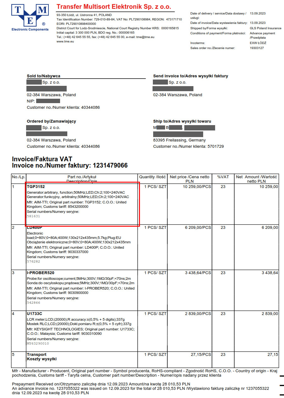
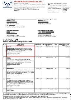
Rechnung von Transfer Multisort Elektronik Sp. z o.o.
Transfer Multisort Elektronik Sp. z o.o. Date of delivery /data dostawy 13.09.2023 Tax Identification Number: VAT No: PL7290108984 Date of invoice/data wystawienia faktury: 13.09.2023 Electronic Components
in „[V] Räumungsverkauf - Alles muss weg!“ · Markt · · Screenshots
-
PDF
xc164_um_v2.1_2004_03_per.pdf
RR w w - - - w w w w w - - w w w w Field Bits Type Description T13STD 15 w Timer T13/T12 Shadow Transfer Disable T12STD 7 0 No action 1 STE13/STE12 is cleared without triggering the shadow transfer T13STR 14 w Timer T13/T12 Shadow Transfer Request T12STR 6 0 No action 1 STE13/STE12 is set, requesting
in „Unterschied Compare match und Period Match“ · Mikrocontroller und Digitale Elektronik ·
-
PDF
DN_047.pdf
ignore this data.) so make sure nothing else is getting triggered. You can poll the SPCR for the SPI Transfer Complete Flag or use an interrupt based routine. Either way once the SPI Transfer is complete the data from the SPDR must be read and stored to a register or ram. I always use an array in RAM and
in „AVR und I/O-Expander“ · Mikrocontroller und Digitale Elektronik ·
-
Datei
gdb.cpp
QString MyBuffer; union __attribute__((__packed__)) { unsigned char Datas[4]; float floatvar; } Transfer; AdressString = QString::number(Adress,16); //Adresse umwandeln MyBuffer = "m" + AdressString +",4"; //16Bit, also 2Byte lesen MyBuffer = generate_RSP_Command(MyBuffer); //Pruefsumme erzeugen MyBuffer
in „Einfacher ARM für den Einstieg und Linux Toolchain“ · Mikrocontroller und Digitale Elektronik ·
-
PDF
Avalon_A3255Q48-131113-V05-EN.pdf
DATA_N stays low and DATA_P transform from low to high and lasts over 125ns, then if no more bit to transfer DATA_P and DATA_N return to high, and bus is back to IDLE state. Figure 3-4 Multi-bit transfer (0Xca) DATA_P High Low DATA_N High Low SEND0 SEND1 SEND0 SEND1 SEND0 SEND0 SEND1 SEND1 IDLE IDLE Figure 3-4 shows bus state when sending 0Xca. Bus could transfer multi-bit without IDLE state inside the transaction, multi-bit transaction start with IDLE state and then transfer data by SEND0 or SEND1. When the transaction finish, it should back to IDLE state
in „Chips für SHA256 Berechnungen“ · Mikrocontroller und Digitale Elektronik ·
-
Datei
Tastertest.asm
Routine für Timer 1 Overflow RJMP TIME0_OVFL ;Routine für Timer 0 Overflow RJMP SPI_HANDLE ;SPI - Transfer beendet RJMP UART_RxC ;UART: Byte empfangen RJMP UART_DRE ;UART: Datenregister leer RJMP UART_TxC ;UART: Transfer beendet RJMP ANA_COMP ;Analog-Komparator ;****************************************
in „Tasten entprellen“ · Mikrocontroller und Digitale Elektronik ·
-
Datei
usart_stm32f4xx.c
(void) { /* Clear DMA Stream Transfer Complete interrupt pending bit */ DMA_ClearITPendingBit(DMA1_Stream6, DMA_IT_TCIF6); static uint_fast16_t readLen = 0; if( DMA1_Stream6->NDTR == 0 ) // Bisheriger Transfer abgeschlossen { DMA_Cmd(DMA1_Stream6, DISABLE); DMA_ITConfig(DMA1_Stream6, DMA_IT_TC, DISABLE); // Bytes vom letzten Transfer entfernen ringbuffer_remove(readLen); // Neuen Block uebertragen readLen = ringbuffer_getReadBlockLength(); DMA1_Stream6->M0AR = (uint32_t) ringbuffer_getReadPtr(); DMA_SetCurrDataCounter(DMA1_Stream6
in „STM32: Sendepuffer für USART“ · Mikrocontroller und Digitale Elektronik ·
-
Datei
spi.c
handled by software SPI_Init(SPI_NUMBER, &SPI_InitStructure); SPI_Cmd(SPI_NUMBER, ENABLE); } } // transfer 1...n bytes in both directions with using the FIFO buffer of the SPI unit --> maximum speed void spi_transfer_block(uint8_t tx_data[], uint8_t rx_data[], uint32_t block_length) { if (block_length
in „SPI Code STM32F103“ · Mikrocontroller und Digitale Elektronik ·
-
PDF
LM94022.pdf
u ■ Battery Management Temperature −50°C to 150°C e ■ Automotive S e Connection Diagram Typical Transfer Characteristic n o SC70-5 Output Voltage vs Temperature r w t h C a s Top View 20143001 s See NS Package Number MAA05A A B O u p u 20143024 t © 2007 National Semiconductor Co201430ion www.national.com
in „Suche nach einem Temperatursensor“ · Mikrocontroller und Digitale Elektronik ·
-
PDF
ST24C32_ST24C64_STM.pdf
receiver. The device that The SDA pin is bi-directional, and is used to trans- controls the data transfer is known as the master, fer data in or out of the memory. It is an open drain and the other as the slave. A data transfer can only output that may be wire-OR’ed with other open be initiated by the
in „I²c mit Bascom und ATmega“ · Mikrocontroller und Digitale Elektronik ·
-
PDF
vti_sca100t-2.pdf
reinitializes the serial communication. • data transfer to MOSI continues immediately after receiving the command in all cases where data is to be written to SCA100T’s internal registers • data transfer out from MISO starts with the falling edge of SCK
in „MSP430 SPI 11BIT !?“ · Mikrocontroller und Digitale Elektronik ·
-
PDF
SCA100T_inclinometer_datasheet_8261800A.pdf
reinitializes the serial communication. • data transfer to MOSI continues immediately after receiving the command in all cases where data is to be written to SCA100T’s internal registers • data transfer out from MISO starts with the falling edge of SCK
in „HCS12 - SPI Schnittstelle programmieren“ · Mikrocontroller und Digitale Elektronik ·
-
PDF
TLC5922.pdf
mA, SOUT 0.5 V V = V or GND, BLANK, XLAT, SCLK, SIN, I Input current I CC –1 1 µA MODE No data transfer, All output OFF, V = 1 V, O 6 R (IREF) 10 k No data transfer, All output OFFO V = 1 V, R = 1.3 k 12 I Supply current (IREF) mA CC Data transfer 30 MHz, All output ON,OV = 1 V, R = 1.3 k 25 (IREF) Data transfer 30 MHz, All output ON,OV = 1 V, (1) R = 600 k 36 65 (IREF) OLC Constant output current All output ON, O = 1 V, (IREF)= 600 70 80 90 mA I Leakage output current All output OFF, O = 15 V, R(IREF) 600
in „daisy-chaining Verzögerung“ · Mikrocontroller und Digitale Elektronik ·
-
PDF
SCA100T_inclinometer_datasheet_8261800A.pdf
reinitializes the serial communication. • data transfer to MOSI continues immediately after receiving the command in all cases where data is to be written to SCA100T’s internal registers • data transfer out from MISO starts with the falling edge of SCK
in „SCA100T-D02 SPI Problem“ · Mikrocontroller und Digitale Elektronik ·
-
PDF
slau144i.pdf
is transferred with one trigger. DMAEN is automatically cleared at the end of the block transfer. 010, 011 Burst-block transfer CPU activity is interleaved with a block transfer. DMAEN is automatically cleared at the end of the burst-block transfer. 100 Repeated single transfer Each transfer
in „Anfängerprogramm TimerA MSP430“ · Mikrocontroller und Digitale Elektronik ·
-
PDF
TLC2543.pdf
in any output format. The internal conversion result is always 12 bits long. When an 8-bit data transfer is selected, the four LSBs of the internal result are discarded to provide a faster one-byte transfer. When a 12-bit transfer is used, all bits are transferred. When a 16-bit transfer is used, four
in „externer A/D Wandler“ · Mikrocontroller und Digitale Elektronik ·
-
PDF
30107090_VA97___ABL322PN___103A.pdf
Figure 9: Drive speed set point reaction time The speed is set according to the Digital control: transfer function PWM input (see Figure 11). 9.4 Digital control: transfer function PWM input The transfer function PWM input is the relation between the Drive speed and the duty cycle on the pin digital PWM
-
 Bild
Bild
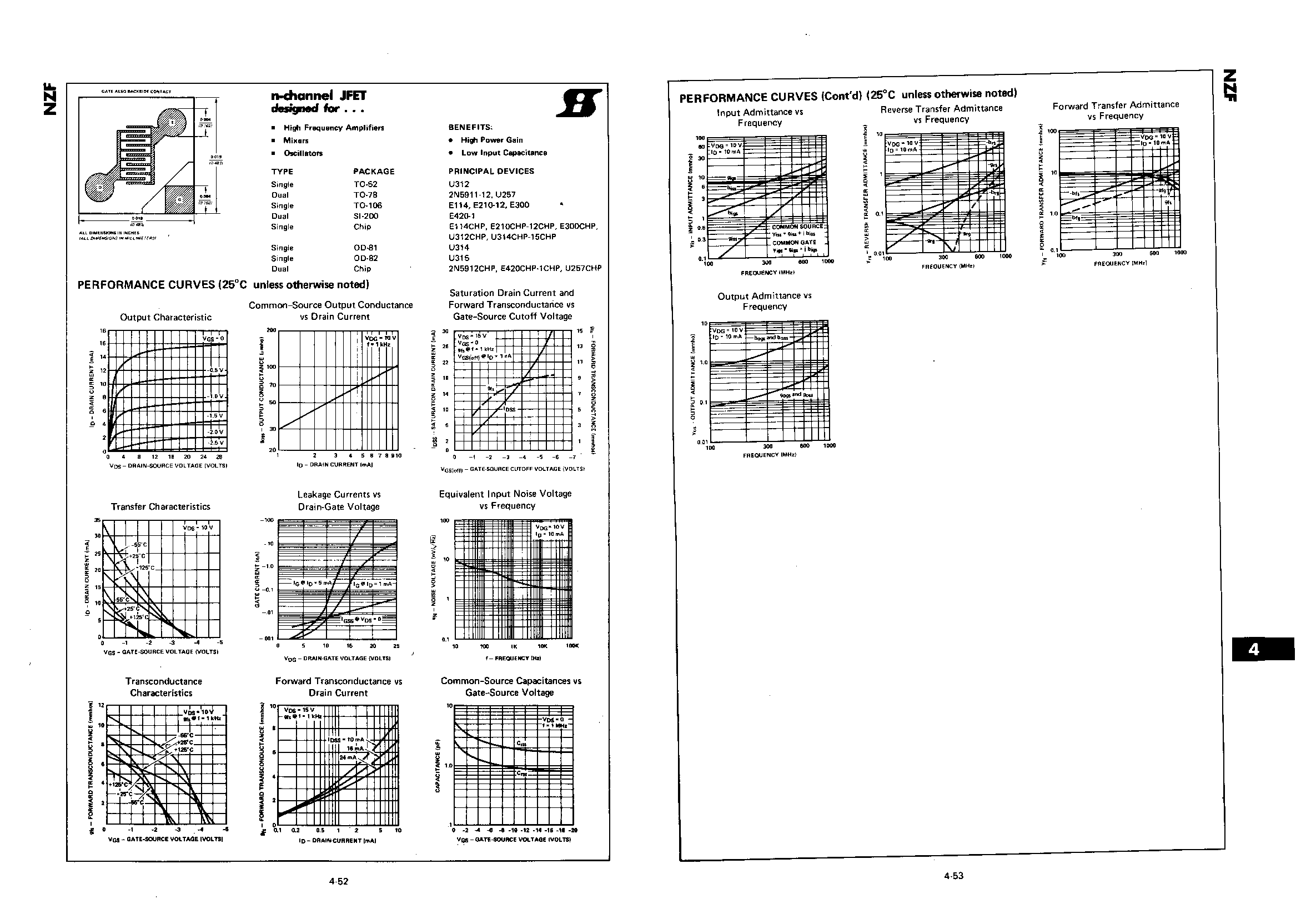
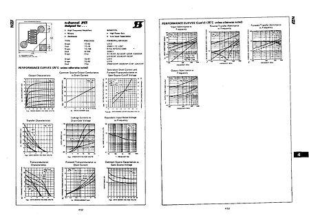
Datenblatt mit Kennlinien von n-Kanal-JFETs
unless otherwise noted) Output Characteristic Common-Source Output Conductance vs Drain Current Transfer Characteristics Leakage Currents vs Drain-Gate Voltage Equivalent Input Noise Voltage vs Frequency Output Admittance vs Frequency Reverse Transfer Admittance vs Frequency Forward Transfer Admittance
in „Leicht unterschiedliche Frequenzen stabil erzeugen“ · Analoge Elektronik und Schaltungstechnik · · Screenshots
-
PDF
EM6126_DS.pdf
SCL fall edge SCL Data stable, data valChange of data allowed Figure 10: Serial interface, 1 bit transfer Transfer data direction is from microcontroller to EM6126. When CS is activated at low level, the communication is enabled and CS must stay low for the rest of the transmission. Data transfer begins
in „LCD mit SPI ansteuern“ · Mikrocontroller und Digitale Elektronik ·
-
PDF
Master-thesis_Wenzel-Maier_final-version.pdf
stage replacement circuit - switch Q8 closed . . . . . . . . . 38 Figure 35 { Pode-plot of the transfer functions i /α (red) and u /α (blue) . 44 Out,1 Out,1 Figure 36 { Full-bridge stage replacement circuit - switch Q7 closed . . . . . . . . . 45 Figure 37 { Pode-plot of the transfer functions i Out
in „Platinfuchs IIa: Isolierter, bidirektionaler 45W DC/DC Wandler zum Laden/Entladen eines Liion-Akkus“ · Projekte & Code ·
-
PDF
LTV815.pdf
LITE-ON TECHNOLOGY CORPORATION Property of LITE-ON Only FEATURES * High current transfer ratio ( CTR : MIN. 600% at I F=1mA, V CE=2V ) * High input-output isolation voltage ( Viso=5,000Vrms ) * Response time ( r: TYP. 60µs at V CE=2V, I C=10mA, R L=100Ω ) * Dual-in-line package : LTV-
in „Mit Optokoppler niederohmig schalten“ · Analoge Elektronik und Schaltungstechnik ·
-
PDF
MOS4007_STM.pdf
60 15 25 50 TLH Transition Time 5 100 200 THL 10 50 100 ns 15 40 80 Minimum and Maximum Voltage Transfer Characterisctics for Inverter and test Circuit Typical Current and Voltage Transfer Characteristics for Inverter and Test Circuit 5/14 HCC/HCF4007UB Typical Voltage Transfer Characteristics for NAND Gate and Test Circuit Typical Voltage Transfer Characteristics for NOR Gate and Test Circuit Typical Output Low (Sink) Current Caracteristics Minimum Output Low (Sink) Current Charac- teristics 6/14 HCC/HCF4007UB Typical Output High (Source) Current
in „Frage zu MOS4007 (MOSFETs + INV)“ · Analoge Elektronik und Schaltungstechnik ·
-
PDF
AutomotiveMOSFETsinLinearApplication-ThermalInstability.pdf
source voltages and thus a higher zero temperature coefficient point (see Figure 4) on the device transfer curve [2]. While the Figure 4. Typical MOSFET transfer characteristic curves over temperature. higher zero temperature coefficient can often be neglected when the applied gate voltage far Application
in „Suche MOSFET mit hohem Rds on“ · Mikrocontroller und Digitale Elektronik ·
-
PDF
AutomotiveMOSFETsinLinearApplication-ThermalInstability.pdf
source voltages and thus a higher zero temperature coefficient point (see Figure 4) on the device transfer curve [2]. While the Figure 4. Typical MOSFET transfer characteristic curves over temperature. higher zero temperature coefficient can often be neglected when the applied gate voltage far Application
in „Linearbetrieb MOSFET gesucht“ · Analoge Elektronik und Schaltungstechnik ·
-
PDF
AutomotiveMOSFETsinLinearApplication-ThermalInstability.pdf
source voltages and thus a higher zero temperature coefficient point (see Figure 4) on the device transfer curve [2]. While the Figure 4. Typical MOSFET transfer characteristic curves over temperature. higher zero temperature coefficient can often be neglected when the applied gate voltage far Application
in „Problem mit N-MOSFET“ · Analoge Elektronik und Schaltungstechnik ·
-
 Bild
Bild
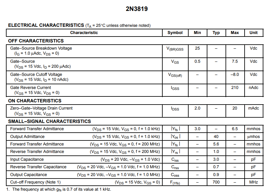
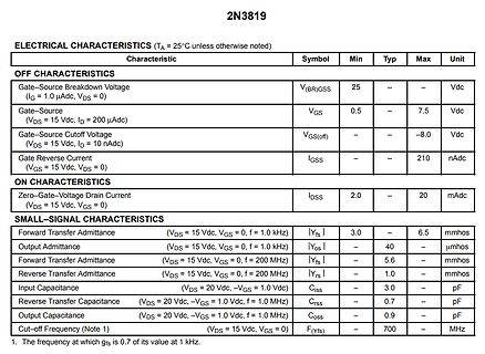
Elektrische Kennwerte des Transistors 2N3819
CHARACTERISTICS Zero-Gate-Voltage Drain Current IDSS 2.0 20 mAdc SMALL-SIGNAL CHARACTERISTICS Forward Transfer Admittance |Yfs| 3.0 6.5 mmhos Output Admittance |Yos| 40 µmhos Reverse Transfer Admittance |Yrs| 1.0 mmhos Input Capacitance |Ciss| 3.0 pF Reverse Transfer Capacitance |Crss| 0.7 pF Output Capacitance
in „[S] Reparatur Analog Messwerk Meter“ · Markt · · Screenshots
-
PDF
TLE5012B_PDS_Rev0.9.pdf
SCKoff 170 - - ns Preliminary Data Sheet 29 V 0.9, 2011-06 TLE5012B Specification 3.5.1.2 SSC Data Transfer The SSC data transfer is word aligned. The following transfer words are possible: • Command word (to access and change operating modes of the TLE5012B) • Data words (any data transferred in any direction) • Safety word (confirms the data transfer and provide status information) wr_delay COMMAND READ Data 1 READ Data2 SAFETY-WORD SSC-Master is driving DATA SSC-Slave is driving DATA Figure 19 SSC data transfer (data read example) wr_delay COMMAND
in „Daten und CRC in Einklang bringen“ · Mikrocontroller und Digitale Elektronik ·
-
PDF
lcd_manual.pdf
CP or fOSC . 409.6 250/270 = 379.2 ms; f CP = 270 kHz.) NOTE When using a 4-bit data length, two transfer operations are needed to transfer a complete data word to or from the external micoprocessor. N: Selects display format (single or dual line). See Table 12 for the correct input value for each model
in „Fehler bei 4Bit LCD Init?“ · Mikrocontroller und Digitale Elektronik ·
-
PDF
lcd-spec.pdf
CP or fOSC . 409.6 250/270 = 379.2 ms; f CP = 270 kHz.) NOTE When using a 4-bit data length, two transfer operations are needed to transfer a complete data word to or from the external micoprocessor. N: Selects display format (single or dual line). See Table 12 for the correct input value for each model
in „LCD Tutorial“ · Mikrocontroller und Digitale Elektronik ·
-
PDF
tsc2003.pdf
leave the data line HIGH to Figure 9: enable the master to generate the STOP condition. • Data transfer may be initiated only when the bus is not busy. Figure 9 details how data transfer is accomplished on the I C bus. Depending upon the state of the R/W bit, two types of • During data transfer, the
in „Touchscreen Controller“ · Analoge Elektronik und Schaltungstechnik ·
-
PDF
lcd_manual.pdf
CP or fOSC . 409.6 250/270 = 379.2 ms; f CP = 270 kHz.) NOTE When using a 4-bit data length, two transfer operations are needed to transfer a complete data word to or from the external micoprocessor. N: Selects display format (single or dual line). See Table 12 for the correct input value for each model
in „LCD will nicht“ · Mikrocontroller und Digitale Elektronik ·
-
PDF
MELEXIS_Sensor-IC-MLX90316KDC_EN.pdf
Design Tria⊗is™ Hall Technology Programmable Angular Range up to 360 Degrees Programmable Linear Transfer Characteristic Selectable Analog (Ratiometric), PWM, Serial Protocol 12 bit Angular Resolution - 10 bit Angular Thermal Accuracy 40 bit ID Number Single Die – SO8 Package RoHS Compliant Dual Die (
in „MLX90316 mit Atmega8 über SPI“ · Mikrocontroller und Digitale Elektronik ·
-
Datei
i2c.asm
brne hh10d_r2 rcall readx ;Receive 4 Bytes (HH10D Parameter) brne hh10d_r2 hh10d_r1: rcall tstop ;Transfer STOP hh10d_r2: rjmp i2cint1 hyt_mr: ;HYT271 MEASURING REQUEST rcall tstop ;Transfer STOP ; ... ;ggf. nächste Funktion initialisieren rjmp i2cint1 hyt_df: ;HYT271 DATA FETCH brts hyt_dft1 ;WIF: No Slave ACK hyt_dft: rcall readx ;Receive 4 Bytes brne i2cint9 hyt_dft1: rcall tstop ;Transfer STOP ; ... ;ggf. nächste Funktion initialisieren i2cint9: rjmp i2cint1 ;I2C Commands ;************ rstart: lds XL,I2CDEV ;Repeated=Read START sez sbrc XL,0 ret ;FINISHED / NOT AVAILABLE sbr XL,1 sts
in „I2C/TWI Master-Interrupt Xmega-Assemblerbaustein“ · Projekte & Code ·
-
Datei
sp2_zynq_wrapper_selftest.c
STAT: 0x%02x\r\n", Xil_In8(baseaddr + SP2_ZYNQ_WRAPPER_MST_STAT_REG_OFFSET)); } xil_printf(" - transfer completed\n\r"); /* Compare the source and destination buffers */ for ( Index = 0; Index < SP2_ZYNQ_WRAPPER_SELFTEST_BUFSIZE; Index++ ) { if ( DstBuffer[Index] != SrcBuffer[Index] ) { xil_printf("
in „ZYNQ: AXI Lite Master Periph um in den DRAM zu schreiben“ · FPGA, VHDL & Co. ·
-
Datei
CIC_IIR.m
cheby2(Cf_amount,attenuation,f); %Chebyshev 2 filter [H_IIR, w] = freqz(b,a,512,"whole"); % return transfer function and frequency in radiant figure('name','IIR Phase') freqz(b,a,512,"whole"); % return transfer function and frequency in radiant %============================= % IIR Filter Plot %=========
in „IIR Filter 2. Ordnung in FPGA implementieren“ · Digitale Signalverarbeitung / DSP / Machine Learning ·
-
PDF
ENG_CS_13C3264_AppNote_0513_Coil_Suppression_Can_Reduce_Relay_Life_13c3264r.pdf
reversed until the flux furtherdecays,finally permitting available spring “return”forces to cause transfer to continue. It is equally important to realize that when the contacts of a typical power 10V/Div. Ref. relay make, connecting very fast rising (e.g., resistive) medium or high current loads to the
in „ESP8266 D1 Mini + Relaismodul: Relais bleibt bei D1 dauerhaft eingeschaltet“ · Mikrocontroller und Digitale Elektronik ·
-
PDF
Part_1_Physical_Layer_Specification_Ver3.01_Final_100218.pdf
attribunes of the communication channel:, Toshiba) and SD Card Association Error-proterted data transfer)hannel • SD Memory Card Form-factork oriented data transfer TmicroSD Memory Card: Specified in "Part 1 microSD Card Addendum" SD Card Addendum" SD Memory onrd).SD Memory Card thickness is defined
in „MicroSD STM32 und Mosfet“ · Mikrocontroller und Digitale Elektronik ·
-
Datei
Arduino_Hitzdrahtanemometer_Bluetooth.ino
/ put your setup code here, to run once: BT.begin(38400); //Serial.begin(9600); // don't use BT-transfer and Serial-transfer to the computer at the same time!!! } void loop() { sensorValue = analogRead(sensorPin); sensorValue = sensorValue * 5.0 / 1023; Serial.println(sensorValue); BT.print(sensorValue); BT.print(";"); // don't forget the semicolon at the end of the data transfer !!! delay(100); }
in „Physikprojekte“ · Offtopic ·
-
PDF
M24CXX.pdf
data to be a receiver. The device that triggers the internal EEPROM write cycle. controls the data transfer is known as the master, Acknowledge Bit (ACK) and the other as the slave. A data transfer can only be initiated by the master, which will also provide An acknowledge signal is used to indicate a successful
in „serielles EEPROM“ · Mikrocontroller und Digitale Elektronik ·
-
PDF
21058F.PDF
device. 3.0 BUS CHARACTERISTICS 3.5 Ac knowledge The following bus protocol has been defined: • Data transfer may be initiated only when the bus Each receiving device, when addressed, is obliged to is not busy. generate an acknowledge after the reception of each • During data transfer, the data line must
-
PDF
mpy100.pdf
X ≤ +10V –10V ≤ Z ≤ +10V ±5.0 ±2.5/1.0 ±1.0 % FSR SQUARER PERFORMANCE Transfer Function (X – X )2 */* * 1 2 + Z 10 2 Total Error –10V ≤ X ≤ +10V ±1.2 ±0.6/0.3 ±0.3 % FSR SQUARE ROOTER PERFORMANCE Transfer Function Z1< Z 2 +√10(Z2– Z 1 + X 2 */* * Total Error 1V ≤ Z ≤ 10V ±2
in „MPY100AG - warum so teuer?“ · Mikrocontroller und Digitale Elektronik ·
-
PDF
ST24C16.pdf
data to be a receiver. The device that triggers the internal EEPROM write cycle. controls the data transfer is known as the master, Acknowledge Bit (ACK) and the other as the slave. A data transfer can only be initiated by the master, which will also provide An acknowledge signal is used to indicate a successful
in „24C16WP - Wie an Mega 16 anschließen?“ · Mikrocontroller und Digitale Elektronik ·
-
 Bild
Bild
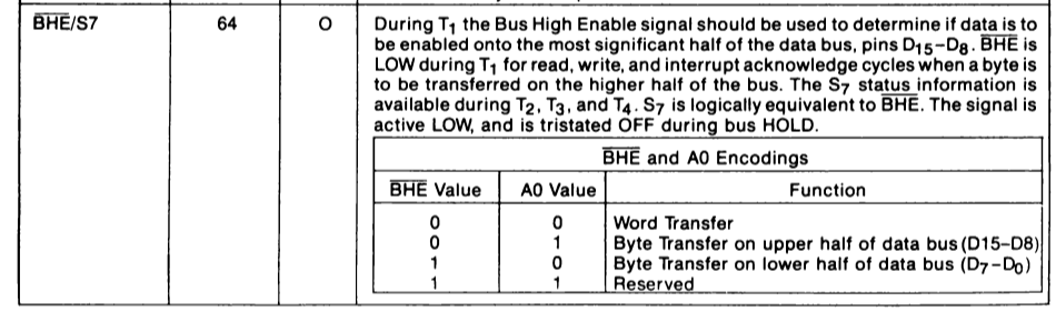
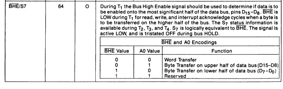
Ausschnitt aus einem Datenblatt zur BHE/S7 Signalbeschreibung
and is tristated OFF during bus HOLD. BHE and A0 Encodings BHE Value A0 Value Function 0 0 Word Transfer 0 1 Byte Transfer on upper half of data bus (D15-D8) 1 0 Byte Transfer on lower half of data bus (D7-D0) 1 1 Reserved
in „Fehlersuche an einem 186er Motherboard (Sinumerik CNC-Steuerung))“ · Mikrocontroller und Digitale Elektronik · · Screenshots
-
 Bild
Bild
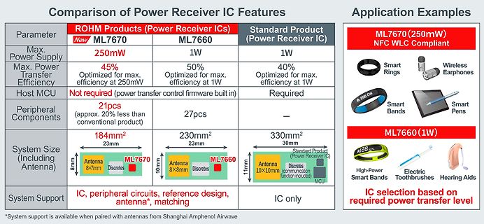
Vergleichstabelle von ROHM Power Receiver IC Features
WLC Compliant ML7660 Standard Product (Power Receiver IC) Parameter Max. Power Supply Max. Power Transfer Efficiency Host MCU Peripheral Components System Size (Including Antenna) System Support 250mW 45% Optimized for max. efficiency at 250mW Not required (power transfer control firmware built in) 21pcs
in „Neue Bauteile: vom Audio-Balun über Transputer bis zum zerstörungsfesten USB-C-Kabel“ · Mikrocontroller und Digitale Elektronik · · Screenshots
-
Datei
hardware_t.cpp
, 0x009AAFF0, 3); break; } case 0x0F : { TransferPlane_Set_Buffer_Adr(0x009569F0, 0x009AAFF0, 0x00000000, 0x00000000); TransferPlanes_clear_asm(0x0093A7F0, 0x0098EDF0, 0x00943DF0, 0x009983F0, 0x0094D3F0, 0x009A19F0, 4); break; } case 0x10 : { TransferPlanes_clear_asm
in „Wittig(welec) DSO W20xxA Open Source Firmware“ · Mikrocontroller und Digitale Elektronik ·
-
PDF
UM10398_-_LPC11xx_UserManual.pdf
transferred in each frame. Values 0000-0010 are not supported and should not be used. 0x3 4-bit transfer 0x4 5-bit transfer 0x5 6-bit transfer 0x6 7-bit transfer 0x7 8-bit transfer 0x8 9-bit transfer 0x9 10-bit transfer 0xA 11-bit transfer 0xB 12-bit transfer 0xC 13-bit transfer 0xD 14-bit transfer 0xE
in „Cortex-M UART im Polling-Betrieb“ · Mikrocontroller und Digitale Elektronik ·
-
Datei
mmctest.c
SPI */ uint8_t sd_write_byte(uint8_t data) { SPDR = data; while(!(SPSR & _BV(SPIF))); /* wait for transfer complete */ return SPDR; } uint8_t sd_read_byte(void) { return sd_write_byte(0xff); } /* send a command */ uint8_t sd_cmd(uint8_t cmdnum, uint32_t arg) { char cmd[6] = { 0x40 | cmdnum, (uint8_t)(arg
in „Zugriffszeit auf SD/MMC über SPI“ · Mikrocontroller und Digitale Elektronik ·
-
PDF
2N5460.pdf
VDS= 15 V, GS = 0, f = 1.0 MHz 5.0 7.0 pF B Crss Reverse Transfer Capacitance VDS= 15 V, GS = 0, f = 1.0 MHz 1.0 2.0 pF F 5 NF Noise Figure VDS= 15 V, GS = 0, 1.0 2.5 dB 4 RG= 1.0 megohm, f = 100 Hz, 6 BW = 1.0 Hz 2 en Equivalent Short-Circuit Input VDS= 15 V, GS
in „Frage zu Ersatztyp für MMBF5460“ · Mikrocontroller und Digitale Elektronik ·
-
PDF
sfh610a-1.pdf
5.3 kVTRIOS Optocoupler High Reliability FEATURES Dimensions in Inches (mm) • Variety of CurrentTransfer Ratios at I =10 FA 2 1 – SFH610A/617A-1, 40–80% pin one ID – SFH610A/617A-2, 63–125% SFH610A – SFH610A/617A-3, 100–200% .255 (6.48) – SFH610A/617A-4, 160–320% .268 (6.81) Anode 1 4 Emitter • Low CTR
in „Frage zu Optokoppler“ · Mikrocontroller und Digitale Elektronik ·
-
Datei
Signal_generator.c
selectPointerXY(cursorStor,1); if (buttondiff&(1<<BUTTON_LEFT)) { if(cursorStor>LEFT_FREQ_END) { transferInstruction(CURSOR_LEFT); if(cursorStor==DECIMAL_POINT_POS+1) {transferInstruction(CURSOR_LEFT);} } } else if (buttondiff&(1<<BUTTON_RIGHT)) { if(cursorStor<RIGHT_FREQ_END) { transferInstruction(CURSOR_RIGHT); if(cursorStor==DECIMAL_POINT_POS-1) {transferInstruction(CURSOR_RIGHT);} } } } void printDouble (double number, uint8_t pos, uint8_t digitsTotal, uint8_t digitsAfterPoint) { char numString[10]; selectPointerXY(pos,1); dtostrf(number, digitsTotal
in „Signalgenerator, Grenzen eines Atmega8“ · Mikrocontroller und Digitale Elektronik ·