-
Thread
St7735 mit STM32F401CCU6
ST77XX_GREEN); delay(1000); tft.fillScreen(ST77XX_BLUE); } void loop(){ digitalWrite(LED_PIN, LOW); delay(500); digitalWrite(LED_PIN, HIGH); delay(500); } ///////////////////////////////////////////////////////////////////// Ich habe auch schon die verschiedenen
-
Thread
PCA9685 I2C Probleme, SCL hängt
zusammen halt nicht lange. Gestern Abend sah ich das bei dem Board mit dem Pico SDA nicht ganz auf low geht (high Pegel 3,3V , low-Pegel 0,5-1,2V). Ich ließ das Board zwei Stunden laufen bis ein Timeout kam. Das Problem hat sich verschlimmert, bis sda schlussendlich 20 Ohm Übergangswiderstand nach 3,3v
Versuche 400kHz, Pegel und Flanken sahen super aus. Bei 3. jedoch das alte Problem (SCl defekt on low oder fast low, nach sekunden oder minuten korrekter Kommunikation). Ich fasste damit das Layout des 3. PCB ins Auge. Ich habe die Leitungen SDA und SCL an den Punkten mit dem schwarzen Kreuz weggeschabt
-
Thread
Z-Diode Laienfrage
Wieso liefert ein Digitalausgang bei LOW 4V?
nun zu > einem permanenten Reset führt. Ich rate mal: Der unbekannte Ausgang kennt 3 Zustände: low, high und floatend. Und der unbekannte Reseteingang hat einen Pullup verbaut, der die 4V liefert.
-
Thread
Raspberry Pi ohne USB-C, neuer OrangePi und neue Messtechnik von Aaronia
Wafer Level Chip Scale Package) with a fine ball pitch of 0.35mm while delivering an industry-leading low operating current of 160nA (typ.). This not only contributes to high-density mounting in space-constrained applications, but also to a significantly extended battery life. Moreover, the TLR1901GXZ features an exceptionally low input offset voltage of just 0.55mV (max.), one of the best among ultra-low current op amps. This represents an approximate 45% reduction compared to typical products on the market. A maximum input
-
Thread
Bluepill mit STLINK/V2 wird mit st-info -probe nicht erkannt
https://www.st.com/en/development-tools/stlink-v3minie.html Kostet 10€ bei Digikey. Ist obendrein HighSpeed USB. Funktioniert einwandfrei. Hat auch noch einen DebugUart mit dabei. fchk
/www.st.com/en/development-tools/stlink-v3minie.html > > Kostet 10€ bei Digikey. Ist obendrein HighSpeed USB. Funktioniert > einwandfrei. Hat auch noch einen DebugUart mit dabei. > > fchk Mit Versand 28€.
-
Thread
MCP2221A springt nicht (auf kommunikation) an
Sebastian V. schrieb im Beitrag #7935961: > [13584.097042] usb 3-2: new low-speed USB device number 22 usin D+ und D- sind vertauscht. Dann taucht ein Full (oder High) Speed Gerät als Low Speed am Bus auf und kann so natürlich nicht vernünftig mit dem Host reden.
Jim M. schrieb im Beitrag #7936690: > Sebastian V. schrieb: >> [13584.097042] usb 3-2: new low-speed USB device number 22 usin > > D+ und D- sind vertauscht. Dann taucht ein Full (oder High) Speed Gerät > als Low Speed am Bus auf und kann so natürlich nicht vernünftig mit dem > Host reden
-
Artikel
NIC
Ausgabe-Pin durch Angabe des Schlüsselwortes "OUTPUT", die Funktion gpio.set() setzt dann den Pin auf HIGH-Pegel, die Funktion gpio.reset() wieder auf LOW-Pegel. Die GPIO-Befehle sind hardware-abhängig und werden deshalb im MINOS-Projekt erklärt. Die Bibliotheksfunktion time.delay() lässt den Mikrocontroller
Code noch vereinfacht werden: Hier wechselt die Funktion gpio.toggle() automatisch den jeweiligen LOW- bzw. HIGH-Pegel und lässt die LED mit einer Frequenz von einem Hertz blinken. Wie wir später noch sehen werden, kann das Blinken der LED auch timergesteuert ausgeführt werden. Dann macht der NIC-Interpreter
-
 Bild
Bild
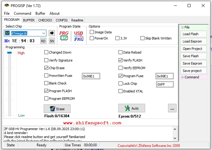
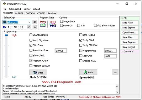
Softwareoberfläche PROGISP für AVR-Mikrocontroller
PRG ISP USB 1010 PRG ID: 1E 94 03 Options Image Data PowerOn 3.3V Skip Blank Written Programming High Changed Down Data Reload Verify Signature Verify FLASH Chip Erase Verify EEPROM Prewritten Fuse 0x99E1 Program Fuse 0x99E1 Blank Check Lock Chip Program FLASH 0XFF Enabled XTAL Program EEPROM Low Erase
-
 Bild
Bild
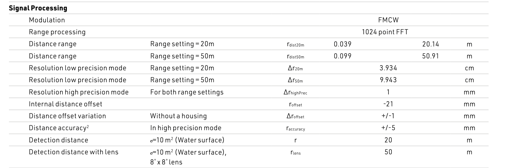
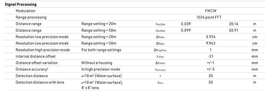
Tabelle mit Spezifikationen zur Signalverarbeitung und Distanzmessung
= 20m rdist20m 0.039 20.14 m Distance range Range setting = 50m rdist50m 0.099 50.91 m Resolution low precision mode Range setting = 20m Δr20m 3.934 cm Resolution low precision mode Range setting = 50m Δr50m 9.943 cm Resolution high precision mode For both range settings ΔrhighPrec 1 mm Internal distance
-
 Bild
Bild
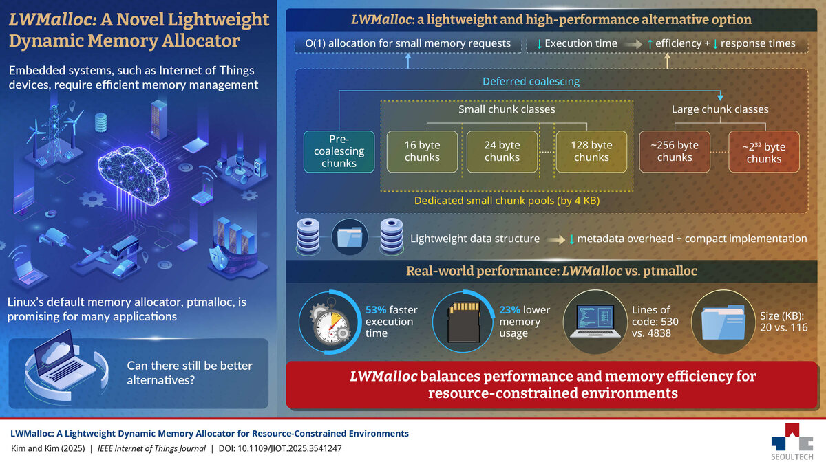
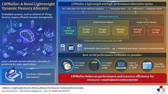
Infografik zum LWMalloc Speicherallokator
promising for many applications Can there still be better alternatives? LWMalloc: a lightweight and high-performance alternative option O(1) allocation for small memory requests -> Execution time -> efficiency -> response times Deferred coalescing Small chunk classes: Pre-coalescing chunks, 16 byte chunks
-
Thread
uC Modul Empfehlung, Tipps für den Aufbau einer Schaltung
Analogeingang zur Auswertung eines Potis. 2 Digitaleingänge für Temperatur-Vorgabe. Beide Eingänge auf LOW bedeutet Wert vom Analogeingang nehmen. Beide Eingänge High bedeutet: Wert vom Poti nehmen. Und die beiden anderen Möglichkeiten rufen 2 Festwerte auf. 1 PWM Ausgang, der über einen Optokoppler und
extern steuern. Aber selbst mit der SPS alleine und ein paar Widerständen und einem Kondensator und "low Speed PWM" habe ich schon recht brauchbare Ergebnisse, um extern "Sparmodus" und "angehobenen Betrieb" nachzubilden und dann z.B. eine dynamische An/Abwesenheitsschaltung per Präsenzmelder zu machen
-
Thread
Schüssel neu ausrichten und anschließen
Sat-Position 19.2E, LO-Frequenzen 9.75/10.6 GHz, Horizontal/Vertikal über die LNB-Versorgungsspannung, Low/High mit 22kHz, kein DiSEqC. Wulf D. schrieb im Beitrag #7933444: > Wenn der LNB vier Abgänge hat, wirst du daran äußerst unterschiedliche > Pegel sehen. Ich nutze den H/L (Horizontal, Low-Frequ
Christoph K. schrieb im Beitrag #7933467: > Wozu gibt es die 22KHz? Umschaltung zwischen Low- und High-Band. Also das, was früher "digitaltauglich" genannt wurde.
-
 Bild
Bild
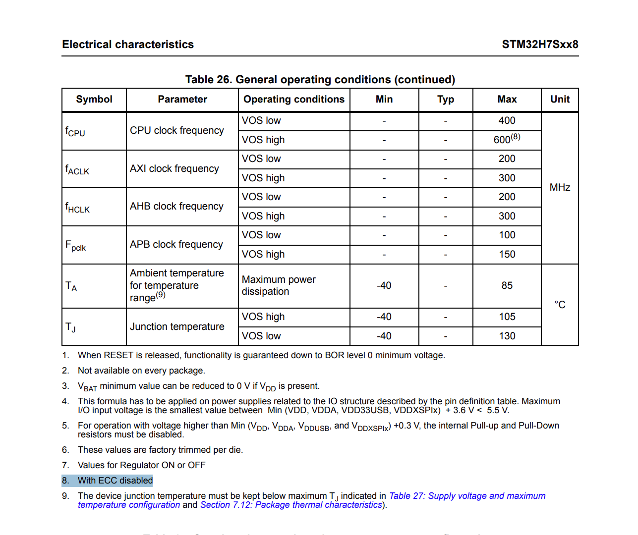
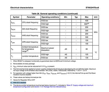
Tabelle der allgemeinen Betriebsbedingungen STM32H7Sxx8
conditions (continued) Symbol Parameter Operating conditions Min Typ Max Unit fCPU CPU clock frequency VOS low - - 400 VOS high - - 600(8) fACLK AXI clock frequency VOS low - - 200 VOS high - - 300 MHz fHCLK AHB clock frequency VOS low - - 200 VOS high - - 300 FPclk APB clock frequency VOS low - - 100 VOS high
-
 Bild
Bild
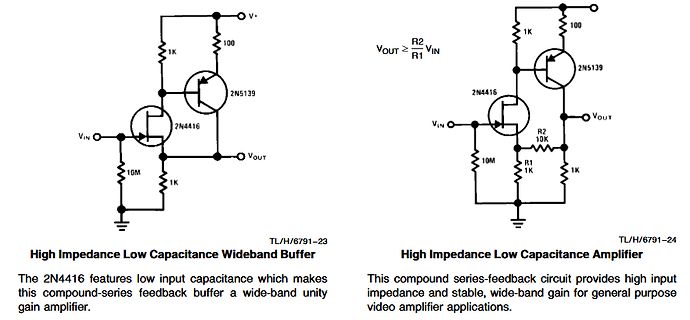
Schaltpläne von Buffer und Verstärker mit Transistoren
V+ 1K 100 2N5139 VIN 2N4416 10M 1K VOUT TL/H/6791-23 High Impedance Low Capacitance Wideband Buffer The 2N4416 features low input capacitance which makes this compound-series feedback buffer a wide-band unity gain amplifier. VOUT >= R2/R1 VIN 1K 2N5139 1K 2N4416 10K R2 10M R1 1K VOUT TL/H/6791-24 High Impedance Low Capacitance Amplifier This compound series-feedback circuit provides high input impedance and stable, wide-band gain for general purpose video amplifier applications.
-
Thread
Richtung des Datenflusses ermitteln?
kann ich inzwischen alles problemlos. Auch die "Elektrik" hat sich geklärt: Ruhepegel um die 3V (High), kurz vor Sendungsbeginn 1 Bitlänge Null (Low), der Rest innerhalb der 8-Byte-Blöcke ganz normale "positive Logik", 1 Bitlänge nach letztem Stopbit wieder Ruhepegel High. SoftSerial vom Arduino hat
-
Thread
CH32V003 HardFault IRQ
BIT_LOW; START_DELAY; for (myCNT=0; myCNT<8; myCNT++) { if (mymcause & 0x00000001UL) BIT_HIGH; else BIT_LOW; mymcause = mymcause>>1; BIT_DELAY; }; BIT_HIGH; BIT_DELAY;
BIT_LOW; START_DELAY; for (myCNT=0; myCNT<8; myCNT++) { if (mymcause & 0x00000001UL) BIT_HIGH; else BIT_LOW; mymcause = mymcause>>1; BIT_DELAY; }; BIT_HIGH; BIT_DELAY;
-
Thread
Positionsanzeige läuft nicht TL7702?
Du findest den Resetpin an Pin 9 des 80C31 Controllers. Der muss nach dem Anschalten kurz mal auf high (+5V) gehen und dann zurück auf 0V. Bei einer Schaltung von 1989 drücke ich dir die Daumen, das der EPROM noch gültige Daten enthält. Verdächtige Bauteile sind in erster Linie die kleinen gelben
80C31: Pin 18 (XTAL2) sollte ~2,5V haben (Quarz schwingt). Pin 9 (Reset) muß low sein Pin 29 (PSEN) ~2,5V (50%, Zugriff auf EPROM) Pin 30 (ALE) ~1,7V (33%, Latchpuls für den 573) Die Encoder gehen vermutlich auf INT0/1 (Pin 12, 13). Wie die LEDs angesteuert werden, ist nicht
-
Thread
Neue Bauteile: Zenerdioden, Steckverbinder, PIC16-Nachwuchs und mehr
1.8V bis 5.5V lebensfähigen Controllerfamilie finden sich folgende Daten zum Stromverbrauch: [c] Low Power Mode Features: – Sleep: • < 900 nA typical @ 3V/25°C (WDT enabled) • < 600 nA typical @ 3V/25°C (WDT disabled) – Operating Current: • 48 μA typical @ 32 kHz, 3V/25°C • < 1 mA typical @ 4
The small sampling capacitors (3.4 pF) maximize input impedance, thus reducing the dependence on high-bandwidth, power-hungry amplifiers typically required by SAR ADCs. [/c] Zu den Wandlerspezifikationen vermeldet man folgendes: [c] Small footprint, big performance • INL: ±0.5 LSB maximum
-
 Bild
Bild
Produktwerbung Xsens Avior OEM Inertial Sensing Lösung
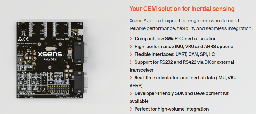
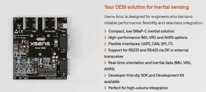
designed for engineers who demand reliable performance, flexibility and seamless integration. Compact, low SwAP-C inertial solution High-performance IMU, VRU and AHRS options Flexible interfaces: UART, CAN, SPI, I2C Support for RS232 and RS422 via DK or external transceiver Real-time orientation and inertial data (IMU, VRU, AHRS) Developer-friendly SDK and Development Kit available Perfect for high-volume integration xsens Avior OEM
-
 Bild
Bild
Datenblatt Ausschnitt RVK Series Strommesswiderstand
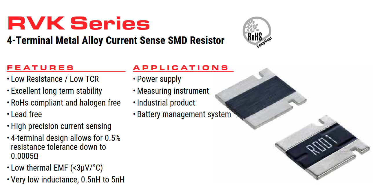
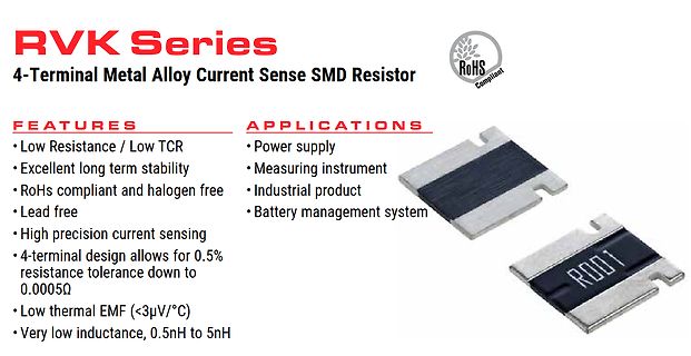
RVK Series 4-Terminal Metal Alloy Current Sense SMD Resistor RoHS Compliant FEATURES • Low Resistance / Low TCR • Excellent long term stability • RoHs compliant and halogen free • Lead free • High precision current sensing • 4-terminal design allows for 0.5% resistance tolerance down to 0.0005Ω • Low thermal EMF (<3µV/°C) • Very low inductance, 0.5nH to 5nH APPLICATIONS • Power supply • Measuring instrument • Industrial product • Battery management system R001
-
 Bild
Bild
Produktfeatures und Anwendungen einer GNSS-Antenne
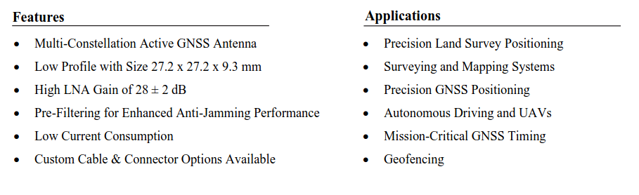
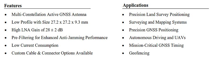
Features Multi-Constellation Active GNSS Antenna Low Profile with Size 27.2 x 27.2 x 9.3 mm High LNA Gain of 28 ± 2 dB Pre-Filtering for Enhanced Anti-Jamming Performance Low Current Consumption Custom Cable & Connector Options Available Applications
-
Thread
AVR128DB USART Transmit Buffer
xl, yh:yl adiw xh:xl, 4 andi xh, 0xF sts extptr+0, xl sts extptr+1, xh subi yl, low(exttrace) sbci yh, high(-exttrace) ldi r16, SLUTRACE_gm | SLUREAD_bm | SLUXCSR_gm | SLUB_bm st Y+, r16 lds r17, USARTA+USART_STATUS_offset st Y+, r17 lds r18, TCB2_CNTL lds
wurde, wird das. 2. Byte aus dem Sendepuffer ins Schieberegister geladen und das DRE Bit geht auf HIGH. Die neuen AVRs haben anscheinend dort 2 Puffer statt bisher einem. Wofür auch immer. Die Testpulse sind absichtlich so breit gemacht, damit man sie einfacher messen und sehen kann. Sind trotzdem
-
 Bild
Bild
Handgezeichneter Schaltplan mit MOSFET und Schalter
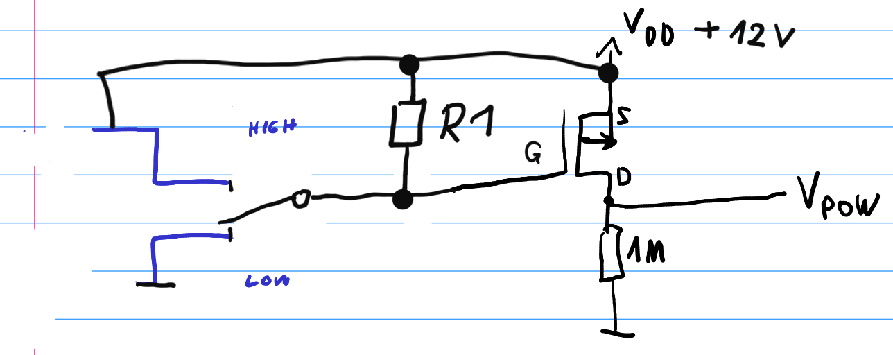
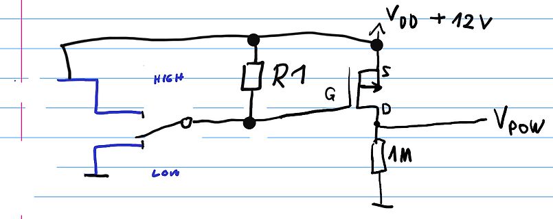
V_DD + 12V R1 HIGH LOW S G D V_POW 1M
-
Thread
Injektorenströme messen Teil 2
Abfall der zu erwarten ist. Bei Einspritzungen ohne den falschen Peak fällt die Spannung auf der Low-Side Leitung e-förmig ab wie zu erwarten. Gemessen hab ich beide Leitungen gegen Masse und dann im Oszilloskop Low-Side von High-Side abgezogen. Strom mit Stromtastkopf. Gemessen hab ich bei Leerlauf
mal Bilder angehängt. Einmal Spannung mit regulärem Verlauf, einmal Spannung mit Peak. Blau ist High-Side, Rot Low Side, Violett die Differenz und damit die am injektor anliegende Spannung, sowie Grün der Strom durch den Injektor. Darüber hinaus sind nochmal die Ströme einzeln aufgezeichnet.
-
Thread
P-MOS Schalter
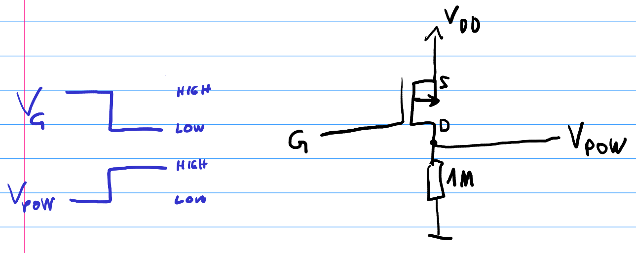
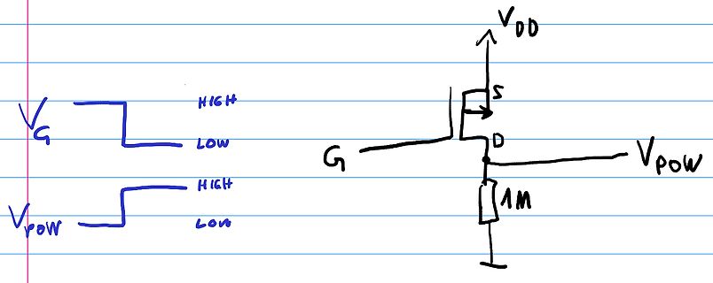
Spannung Gate-Source relevant (Ugs). Hmm da dachte ich eigentlich, dass das passt. VDD ist immer HIGH, sprich sobald VG LOW ist, dachte ich schaltet der PMOS durch.
Tom M. schrieb im Beitrag #7932332: > VDD ist immer HIGH, sprich sobald VG LOW ist, dachte ich schaltet der > PMOS durch. Das ist auch so. Wichtig ist nur, dass das high Signal genauso groß ist wie VDD, damit der MOSFET vernünftig sperrt! Wenn du gewährleisten
-
 Bild
Bild
Schaltplan mit MOSFET und Signalkurven
VG HIGH LOW VPOW HIGH LOW S D G VPOW 1M
-
Thread
Mini Whip Antenne FA, warum MOSFET statt jFET?
Schaltung findet sich auf Seite 8 in der alten National Semiconductor (heute TI) Application Note als "High Impedance Low Capacitance Wideband Buffer": https://www.ti.com/lit/an/snoa620/snoa620.pdf?ts=1757000828402 Auszug daraus im angehängten Bild: links mit 100% Gegenkopplung, rechts mit geteilter
-
Thread
Entlötstation mittleres Preissegment / Kaufberatung
SolderingMFG verknüpft ATTEN und ATETOOL (https://solderingmfg.com/pages/about). Ich vermute ATETOOL soll den Low-End Markt bedienen, während Atten in den High-End Markt will. ATETOOL wird ebenfalls von Reichelt verkauft, aber eine ATETOOL Entlötstation habe ich nicht gesehen. Bleibt die teure Atten-Station
-
 Bild
Bild
Tabelle mit Leistungsdaten und Formeln eines Datenblatts
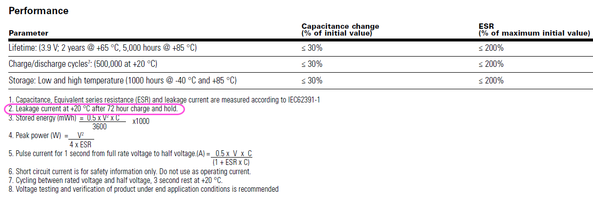
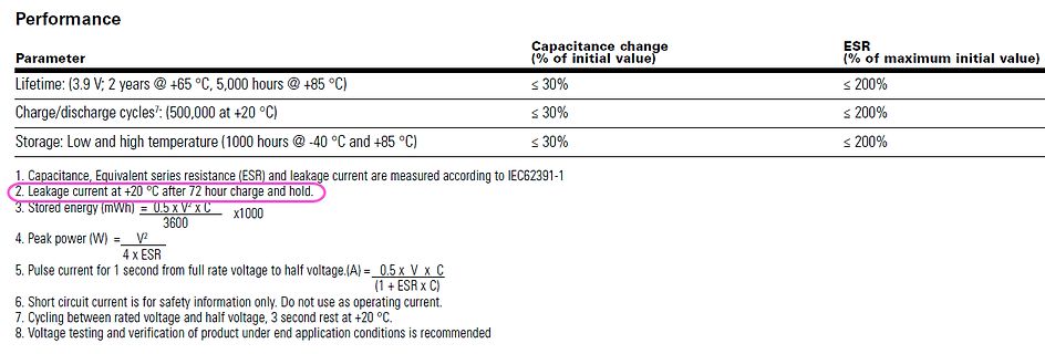
5,000 hours @ +85 °C) ≤ 30% ≤ 200% Charge/discharge cycles: (500,000 at +20 °C) ≤ 30% ≤ 200% Storage: Low and high temperature (1000 hours @ -40 °C and +85 °C) ≤ 30% ≤ 200% 1. Capacitance, Equivalent series resistance (ESR) and leakage current are measured according to IEC62391-1 2. Leakage current at +
-
Thread
Armbian-Update, Espressif-Devcon, STMicroelectronics-Kameramodul uvam
/attachment/677634/7.png) Bildquelle: https://www.mill-max.com/products/new/mill-max-introduces-low-force-spring-options-for-high-reliability-spring-loaded-interconnects MillMax kündigte nun eine „neue“ Serie an, die mit schwächeren Federn ausgestattet ist. Als Ursache für diese auf den ersten Blick widersinnig erscheinende Veränderung wird folgendes angeführt: [c] Typically, higher force spring pins are used to ensure reliable electrical performance, however, there are cases where lower spring force may be advantageous and required. For example, high pin count arrays found in
-
 Bild
Bild
Präsentationsfolie über Herausforderungen in Embedded Vision
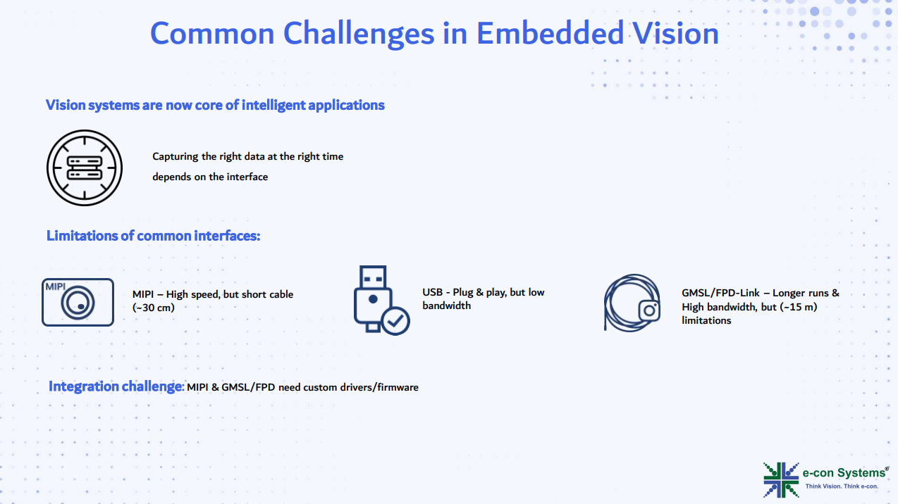
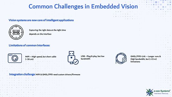
the right data at the right time depends on the interface Limitations of common interfaces: MIPI – High speed, but short cable (~30 cm) USB – Plug & play, but low bandwidth GMSL/FPD-Link – Longer runs & High bandwidth, but (~15 m) limitations Integration challenge: MIPI & GMSL/FPD need custom drivers/
-
Thread
ili9341 2.8 Zoll Modul Problem
{ uint8_t d; do { #if ili_bitbang d = *buff++; if (d & 0x80)ll_mosi_high; else ll_mosi_low; // bit7 ll_ck_cycle; if (d & 0x40)ll_mosi_high; else ll_mosi_low; // bit6 ll_ck_cycle; if (d & 0x20)ll_mosi_high; else ll_mosi_low; // bit5 ll_ck_cycle; if (d & 0x10)ll_mosi_high; else ll_mosi_low; // bit4 ll_ck_cycle; if (d & 0x08)ll_mosi_high; else ll_mosi_low; // bit3 ll_ck_cycle; if (d & 0x04)ll_mosi_high; else ll_mosi_low; // bit2 ll_ck_cycle