Suchergebnisse für "555"
------------ .def lpm00 = r00 ;lpm00:reserved for lpm .def keymain = r01 ;aux01:main_keys .def ckne555 = r02 ;aux02:clock_ne555 .def keyaux = r03 ;aux03:aux_keys .def keyfbck = r04 ;aux04:function+bck_keys .def swbcd01 = r05 ;aux05:switch_bcd0+1 .def swbcd23 = r06 ;aux06:switch_bcd2+3 .def aux07 = r07
in
„meinungen zu ass.prog.“
·
Mikrocontroller und Digitale Elektronik
·
11.10.2006 12:56
------------ .def lpm00 = r00 ;lpm00:reserved for lpm .def keymain = r01 ;aux01:main_keys .def ckne555 = r02 ;aux02:clock_ne555 .def keyaux = r03 ;aux03:aux_keys .def keyfbck = r04 ;aux04:function+bck_keys .def swbcd01 = r05 ;aux05:switch_bcd0+1 .def swbcd23 = r06 ;aux06:switch_bcd2+3 .def aux07 = r07
in
„Problem bei Tasterabfrage“
·
Mikrocontroller und Digitale Elektronik
·
11.10.2006 12:59
Set We Reset Oe Waitus 10 Daten = Dataport Waitus 10 Set Oe Waitus 10 Return Send11to1: Adresse = &H555 Daten = &HAA Gosub Writef Adresse = &H2AA Daten = &H55 Gosub Writef Adresse = &H555 Daten = &HA0 Gosub Writef Adresse = &H01 Daten = &H11 Gosub Writef Return Chiperase: Adresse = &H555 Daten = &HAA Gosub Writef Adresse = &H2AA Daten = &H55 Gosub Writef Adresse = &H555 Daten = &H80 Gosub Writef Adresse = &H555 Daten = &HAA Gosub Writef Adresse = &H2AA Daten = &H55 Gosub Writef Adresse = &H555 Daten = &HAA Gosub Writef Return
in
„Hilfe bei 29f040 programmierung mit avr“
·
Mikrocontroller und Digitale Elektronik
·
01.11.2006 13:27
3rd 4th 5th 6th L Addr Data Addr Data Addr Data Addr Data Addr Data Addr Data 1 X F0 Read/Reset 3 555 AA 2AA 55 X F0 Auto Select 3 555 AA 2AA 55 555 90 Program 4 555 AA 2AA 55 555 A0 PA PD Unlock Bypass 3 555 AA 2AA 55 555 20 Unlock Bypass 2 X A0 PA PD Program Unlock Bypass Reset 2 X 90 X 00 Chip Erase 6 555 AA 2AA 55 555 80 555 AA 2AA 55 555 10 Block Erase 6+ 555 AA 2AA 55 555 80 555 AA 2AA 55 BA 30 Erase Suspend 1 X B0 Erase Resume 1 X 30 Table 8. Commands, 8-bit mode, BYTE = V IL h Bus Write Operations
in
„AT91 & OpenOCD Externes Flash Problem“
·
Mikrocontroller und Digitale Elektronik
·
08.08.2007 09:16
3rd 4th 5th 6th L Addr Data Addr Data Addr Data Addr Data Addr Data Addr Data 1 X F0 Read/Reset 3 555 AA 2AA 55 X F0 Auto Select 3 555 AA 2AA 55 555 90 Program 4 555 AA 2AA 55 555 A0 PA PD Unlock Bypass 3 555 AA 2AA 55 555 20 Unlock Bypass 2 X A0 PA PD Program Unlock Bypass Reset 2 X 90 X 00 Chip Erase 6 555 AA 2AA 55 555 80 555 AA 2AA 55 555 10 Block Erase 6+ 555 AA 2AA 55 555 80 555 AA 2AA 55 BA 30 Erase Suspend 1 X B0 Erase Resume 1 X 30 Table 8. Commands, 8-bit mode, BYTE = V IL h Bus Write Operations
in
„Externes Flash M29F400B ansprechen“
·
Mikrocontroller und Digitale Elektronik
·
11.10.2006 13:23
Return Chiperase: Adresse = &H555 Daten = &HAA Gosub Writef Adresse = &H2AA Daten = &H55 Gosub Writef Adresse = &H555 Daten = &H80 Gosub Writef Adresse = &H555 Daten = &HAA Gosub Writef Adresse = &H2AA Daten = &H55 Gosub Writef Adresse = &H555 Daten = &H10 Gosub Writef For Adresse = 0 To 65535 Do Gosub Readf Loop Until Daten = 255 Next c Return
in
„M32 Bascom Programm zum Beschreiben von AM29F040 Flash“
·
Projekte & Code
·
01.11.2006 21:57
------------ .def lpm00 = r00 ;lpm00:reserved for lpm .def keymain = r01 ;aux01:main_keys .def ckne555 = r02 ;aux02:clock_ne555 .def keyaux = r03 ;aux03:aux_keys .def keyfbck = r04 ;aux04:function+bck_keys .def swbcd01 = r05 ;aux05:switch_bcd0+1 .def swbcd23 = r06 ;aux06:switch_bcd2+3 .def aux07 = r07
in
„Problem bei Tasterabfrage“
·
Mikrocontroller und Digitale Elektronik
·
11.10.2006 12:59
------------ .def lpm00 = r00 ;lpm00:reserved for lpm .def keymain = r01 ;aux01:main_keys .def ckne555 = r02 ;aux02:clock_ne555 .def keyaux = r03 ;aux03:aux_keys .def keyfbck = r04 ;aux04:function+bck_keys .def swbcd01 = r05 ;aux05:switch_bcd0+1 .def swbcd23 = r06 ;aux06:switch_bcd2+3 .def aux07 = r07
in
„Takt oder Beat aus Musik filtern“
·
Mikrocontroller und Digitale Elektronik
·
11.10.2006 13:01
------------ .def lpm00 = r00 ;lpm00:reserved for lpm .def keymain = r01 ;aux01:main_keys .def ckne555 = r02 ;aux02:clock_ne555 .def keyaux = r03 ;aux03:aux_keys .def keyfbck = r04 ;aux04:function+bck_keys .def swbcd01 = r05 ;aux05:switch_bcd0+1 .def swbcd23 = r06 ;aux06:switch_bcd2+3 .def aux07 = r07
in
„wieso wird andauernd int0 und int1 ausgelöst?“
·
Mikrocontroller und Digitale Elektronik
·
11.10.2006 13:02
------------ .def lpm00 = r00 ;lpm00:reserved for lpm .def keymain = r01 ;aux01:main_keys .def ckne555 = r02 ;aux02:clock_ne555 .def keyaux = r03 ;aux03:aux_keys .def keyfbck = r04 ;aux04:function+bck_keys .def swbcd01 = r05 ;aux05:switch_bcd0+1 .def swbcd23 = r06 ;aux06:switch_bcd2+3 .def aux07 = r07
in
„stacksicherung bei 2 ints“
·
Mikrocontroller und Digitale Elektronik
·
11.10.2006 13:02
Bild
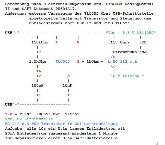
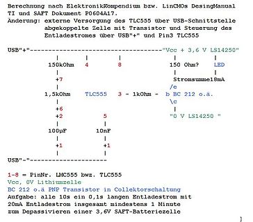
ElektronikKompendium bzw. LinCMOs DesingManual TI und SAFT Dokument P0604A17. Änderung: externe Versorgung des TLC555 über USB-Schnittstelle abgekoppelte Zelle mit Transistor und Steuerung des Entladestromes über USB+" und Pin3 TLC555 . USB"+"---...Vcc + 3,6V LS14250" 150kOhm 4 8 150 Ohm? LED | +7 | Stromsumme 18mA 1,5kOhm TLC555 3 - 1kOhm - b BC 212 o.ä. | /e | \c | +6 5 | 0 V LS14250 | +2 10nF | | +1 100uF | +1 | USB"---... 1-8 = PinNr. LMC555 bzw. TLC555 . Vcc, 0V Lithiumzelle. BC 212 o.ä PNP Transistor in Kollektorschaltung
in
„Astabiler Multivibrator mit TLC555 (LMC555)“
·
Analoge Elektronik und Schaltungstechnik
·
02.06.2024 20:37
·
Screenshots
Bild
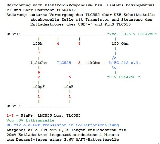
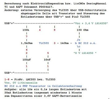
ElektronikKompendium bzw. LinCMOs DesingManual
TI und SAFT Dokument P0604A17.
Änderung: externe Versorgung des TLC555 über USB-Schnittstelle
abgekoppelte Zelle mit Transistor und Steuerung des
Entladestromes über USB"+" und Pin3 TLC555
USB"+" ----------------------------------- "Vcc + 3,6 V LS14250"
| 150k | 4 | 8 | 150 Ohm
| 7 | | | /e
1,5kohm TLC555 3 - 1kohm - b BC 212 o.ä.
| 6 | | | \c
2 | | | "0 V LS14250"
100µF 5 10nF
| 1 | | 1
USB"-" -----------------------------------
1-8 = PinNr. LMC555 bzw. TLC555
Vcc, 0V Lithiumzelle
BC 212 o.ä PNP Transistor
in
„Astabiler Multivibrator mit TLC555 (LMC555)“
·
Analoge Elektronik und Schaltungstechnik
·
02.06.2024 09:07
·
Screenshots
------------ .def lpm00 = r00 ;lpm00:reserved for lpm .def keymain = r01 ;aux01:main_keys .def ckne555 = r02 ;aux02:clock_ne555 .def keyaux = r03 ;aux03:aux_keys .def keyfbck = r04 ;aux04:function+bck_keys .def swbcd01 = r05 ;aux05:switch_bcd0+1 .def swbcd23 = r06 ;aux06:switch_bcd2+3 .def aux07 = r07
in
„Takt oder Beat aus Musik filtern“
·
Mikrocontroller und Digitale Elektronik
·
11.10.2006 13:01
------------ .def lpm00 = r00 ;lpm00:reserved for lpm .def keymain = r01 ;aux01:main_keys .def ckne555 = r02 ;aux02:clock_ne555 .def keyaux = r03 ;aux03:aux_keys .def keyfbck = r04 ;aux04:function+bck_keys .def swbcd01 = r05 ;aux05:switch_bcd0+1 .def swbcd23 = r06 ;aux06:switch_bcd2+3 .def aux07 = r07
in
„stacksicherung bei 2 ints“
·
Mikrocontroller und Digitale Elektronik
·
11.10.2006 13:02
R40 N Z 1 G F KFZ+1 1 OUT +5V These Caps are connected between KFZ Ground Plane Connector for BTS 555 2 IN BTS555 and Battery Ground Plane on PCB. to screw the tab to board 3 K They are intended to AC couple the two ground Planes VBB I 1 C48 C43 C44 4 ST U6 T S Maybe this is unecessary I KFZOUT 5 A
in
„Akku und Wasserstandsdisplay für Wohnmobile“
·
Projekte & Code
·
21.06.2016 11:51
R40 N Z 1 G F KFZ+1 1 OUT +5V These Caps are connected between KFZ Ground Plane Connector for BTS 555 2 IN BTS555 and Battery Ground Plane on PCB. to screw the tab to board 3 K They are intended to AC couple the two ground Planes VBB I 1 C48 C43 C44 4 ST U6 T S Maybe this is unecessary I KFZOUT 5 A
in
„Akku und Wasserstandsdisplay für Wohnmobile“
·
Projekte & Code
·
21.06.2016 14:16
/ s (Note 11) 555 X02 0001 t A Indicator Bits 4 555 AA 2AA 55 (BA) 90 (BA) (Note 555 X03 12) Program 4 555 AA 2AA 55 555 A0 PA Data Chip Erase 6 555 AA 2AA 55 555 80 555 AA 2AA 55 555 10 Sector Erase 6 555 AA 2AA 55
in
„PHILIPS VP5500 VoIP Telefon bei Pollin“
·
Mikrocontroller und Digitale Elektronik
·
13.03.2010 12:10
Kurvenverlauf bezieht sich auf die in Bild 5 verdeutlichte funkti- bzw. bipolaren Ausführung des NE555 jeweils ca. 5 kOhm. Die onstheoretische Grundlage. Die Gerade (gelb) zeigt den Leistungsverlauf von verschiedenen Herstellern produzierten C-MOS-Varianten über eine einstellbare Gleichspannungsquelle
in
„12 Volt Motor mit 48 Volt Netzteil betreiben. Geht das durch PWM?“
·
Analoge Elektronik und Schaltungstechnik
·
21.07.2019 10:27
the device. This is a three step from LOW from LOW operation: the first address/data combination is 555 [H]/ to HIGH to HIGH AA[H];thesecondcombinationis2AA[H]/55[H];andthe May change Will change from HIGH from HIGH final command combination is 555 [H]/33[H]. This se- to LOW to LOW quence of pseudo write
in
„[VS] verschenke 2x NVRAM Xicor X20C16“
·
Markt
·
12.08.2021 11:16
55 90 e Byte AAA 555 AAA X02 AB o (SA) XX00 u Word 555 2AA 555 A Sector Protect Verify X02 XX01 (Note 9) 4 AA 55 90 00 Byte AAA 555 AAA (SA) X04 01 Program Word 4 555 AA 2AA 55 555 A0 PA PD Byte AAA 555 AAA Word 555 2AA 555 555 2AA 555 Chip Erase Byte 6 AAA AA 555 55 AAA 80 AAA AA 555 55 AAA 10 Word 555 2AA 555 555 2AA Sector Erase Byte 6 AAA AA 555 55 AAA 80 AAA AA 555 55 SA 30 Erase Suspend (Note 10) 1 XXX B0 Erase Resume
in
„AT91 & OpenOCD Externes Flash Problem“
·
Mikrocontroller und Digitale Elektronik
·
08.08.2007 14:56
222 chip or two elements of 1 Introduction In 1971, the Swiss electrical engineer and inventor the 555 chip (556 chip). Hans Rudolf Camenzind (1934-2012), under a contract with Signetics Corporation (USA), then Philips (the Netherlands), developed a universal integrated chip-timer 555 (The IC Time Machine), designed for the formation of single and repeated pulses. The timer 555 contains two analog comparators, an asynchronous RS trigger, a resistive voltage divider and a number of other elements [1-3]. The IC 555 and its many analogues used to create timers, generators, devices
in
„Chip 222 - alternative 555“
·
Analoge Elektronik und Schaltungstechnik
·
01.04.2024 12:09
--------;auxiliary_register .def lpm00 = r00 ; lpm00 .def keymain = r01 ; aux01:main_keys .def ckne555 = r02 ; aux02:clock_ne555 .def keyaux = r03 ; aux03:aux_keys .def keyfbck = r04 ; aux04:function+bck_keys .def swbcd01 = r05 ; aux05:switch_bcd0+1 .def swbcd23 = r06 ; aux06:switch_bcd2+3 .def aux07
in
„meinungen zu ass.prog.“
·
Mikrocontroller und Digitale Elektronik
·
11.10.2006 12:56
Bild
over operating free-air temperature range (unless otherwise noted)
MIN MAX UNIT
VCC Supply voltage NA555 , NE555 , SA555 4.5 16 V
SE555 4.5 18
IO Output current ±200 mA
in
„NE555 wird heiß“
·
Mikrocontroller und Digitale Elektronik
·
06.03.2025 08:27
·
Screenshots
Bild
over operating free-air temperature range (unless otherwise noted)
MIN MAX UNIT
VDD Supply voltage
TLC555 C 2 15 V
TLC555 I 3 15 V
TLC555 M 5 15 V
TLC555 Q 5 15 V
in
„Astabiler Multivibrator mit TLC555 (LMC555)“
·
Analoge Elektronik und Schaltungstechnik
·
30.05.2024 10:22
·
Screenshots
wohl die Erzeugung eines 5min Takts mit einem als astabilen Multivibrator beschalteten Timer IC NE555 /LM555 (oder besser dessen modernere CMOS Variante LMC555 /TLC555 /ICM7555) sein. Laut Datenblatt braucht für die korrek- te Funktion des ZN427 auch nicht unbedingt ein Monoflop zur Verkürzung des LOW
in
„Impulsgeber für 8 bit ADU“
·
Mikrocontroller und Digitale Elektronik
·
11.10.2006 17:45
4.5 ICL7129 TL062 TL062 CD4011 ICM7555 TL062 LM358 ICL8069 2-44a 37 216 DM8045 4.5 ICL7135 74LS247 NE555 LM399H ICL7650 LF411 LM358 LF412 7805 7805 7912? 7912 2-44b 216 GDM8045 4.5 ICL7135 74LS247 NE555 LM399H ICL7650 LF411 LM358 LF412 7805 7805 7912? 7912 2-44c 216 DM8045A 4.5 ICL7135 74LS247 NE555 LM399H ICL7650 LF411 LM358 LF412 7805 7805 7912? 7912 2-44d 216 DM8145A 4.5 ICL7135 74LS247 NE555 LM399H ICL7650 LF411 LM358 LF412 7805 7805 7912? 7912 2-44e 38 216 VC8145 4.5 ICL7135 74LS247 NE555 LM399H ICL7650 LF411 LM358 LF412 AD637 7805 7805 7812 7912 2-24 39 141 PF24A 3.5 ICL7106 TL062 CD4070
in
„Suche Schaltplan / Bed-Anleitung Mastech M840D DMM gute Qualität“
·
Mikrocontroller und Digitale Elektronik
·
25.10.2017 14:43
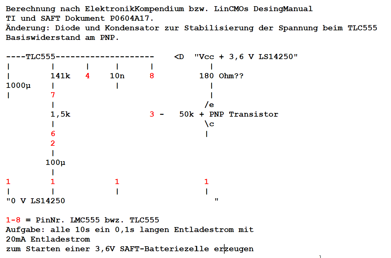
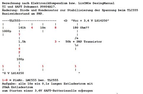
Bild
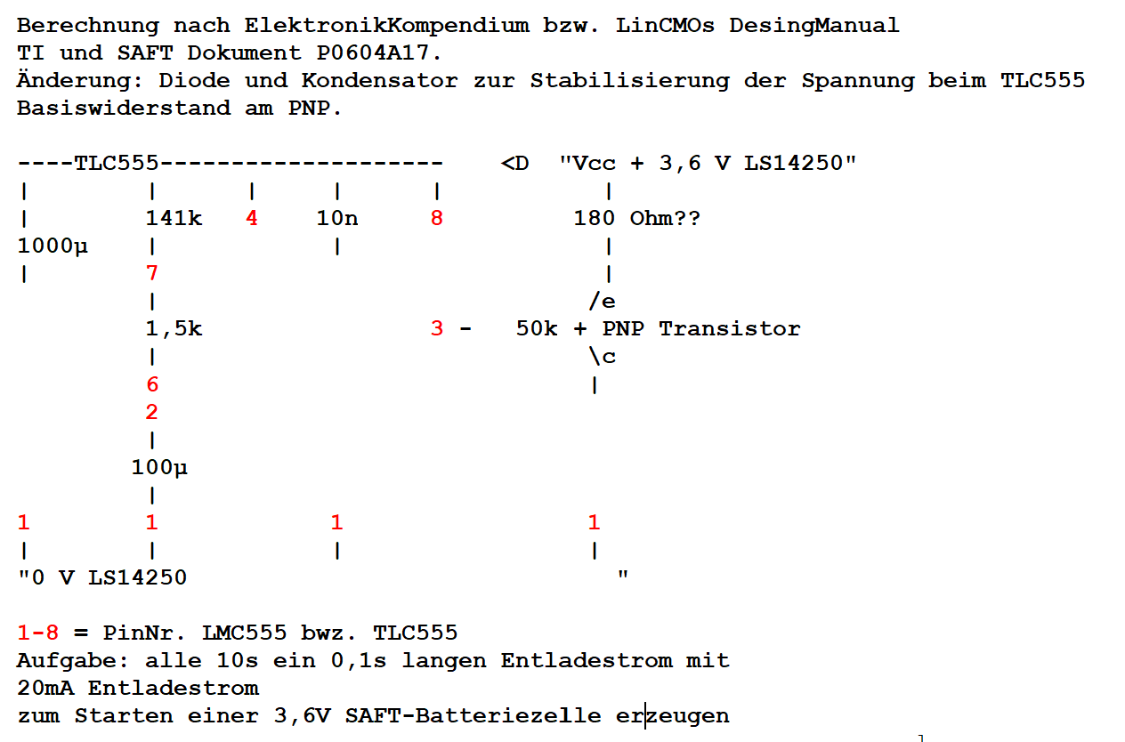
und SAFT Dokument P0604A17.
Änderung: Diode und Kondensator zur Stabilisierung der Spannung beim TLC555
Basiswiderstand am PNP.
----TLC555 -------------------- <D "Vcc + 3,6 V LS14250"
| | 4 10n 8 180 Ohm??
1000µ | | | 7 | /e
| 1,5k 3 - 50k + PNP Transistor
| | \c
6 | |
2 | |
100µ | |
1 1 1
"0 V LS14250"
1-8 = PinNr. LMC555 bzw. TLC555
Aufgabe: alle 10s ein 0,1s langen Entladestrom mit 20mA Entladestrom zum Starten einer 3,6V SAFT-Batteriezelle erzeugen
in
„Astabiler Multivibrator mit TLC555 (LMC555)“
·
Analoge Elektronik und Schaltungstechnik
·
30.05.2024 04:33
·
Screenshots
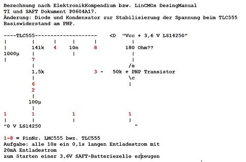
Bild
und SAFT Dokument P0604A17.
Änderung: Diode und Kondensator zur Stabilisierung der Spannung beim TLC555
Basiswiderstand am PNP.
----TLC555 -------------------- <D "Vcc + 3,6 V LS14250"
| | 4 10n 8 180 Ohm??
1000µ | | | 7 | /e
| 1,5k 3 - 50k + PNP Transistor
| | \c
6 | |
2 | |
100µ | |
1 1 1
"0 V LS14250"
1-8 = PinNr. LMC555 bzw. TLC555
Aufgabe: alle 10s ein 0,1s langen Entladestrom mit 20mA Entladestrom zum Starten einer 3,6V SAFT-Batteriezelle erzeugen
in
„Astabiler Multivibrator mit TLC555 (LMC555)“
·
Analoge Elektronik und Schaltungstechnik
·
30.05.2024 05:12
·
Screenshots
(SA)X04 Word 555 2AA 555 Enter SecSi Sector Region Byte 3 AAA AA 555 55 AAA 88 Word 555 2AA 555 Exit SecSi Sector Region Byte 4 AAA AA 555 55 AAA 90 XXX 00 Word 555 2AA 555 Program Byte 4 AAA AA 555 55 AAA A0 PA PD Word 555 2AA 555 Unlock Bypass Byte 3 AAA AA 555 55 AAA 20 Unlock Bypass Program (Note 11) 2 XXX A0 PA PD Unlock Bypass Reset (Note 12) 2 XXX 90 XXX 00 Word 555 2AA 555 555 2AA 555 Chip Erase 6 AA 55 80 AA 55
in
„55 Stk. Flashbausteine 32Mbit, TSSOP48, 3,3V AM29DL323DB-90“
·
Markt
·
09.01.2008 11:41
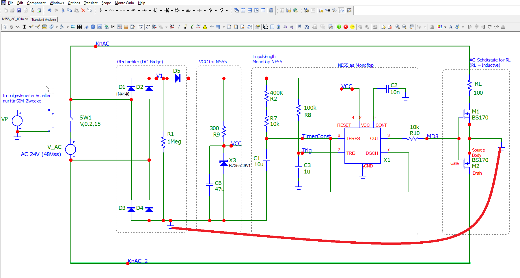
Bild
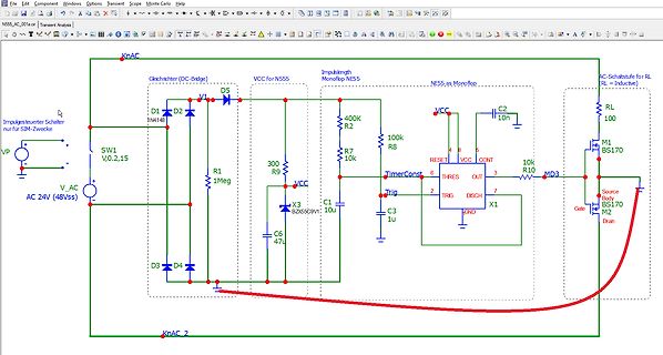
File Edit Component Windows Options Transient Analysis Scope Monte Carlo Help N555 _AC_001a Transient Analysis KnAC Gleichrichter (DC-Bridge) D1 D2 V1 3N4148 D5 VCC for N555 Impulslength Monoflop NE555 400K R2 100K R8 7k R7 10k C2 10n NE555 as Monoflop VCC RESET THRES OUT CONT 10k
in
„Mosfets als Klein-(wechsel)-spannung-Schalter“
·
Analoge Elektronik und Schaltungstechnik
·
09.10.2022 01:39
·
Screenshots
*********;auxiliary_register .def lpm00 = r00 ; lpm00 .def keymain = r01 ; aux01:key_main .def ckne555 = r02 ; aux02:clock_ne555 .def keyaux = r03 ; aux03:key_aux .def keyfbck = r04 ; aux04:key_function+bck .def swbcd01 = r05 ; aux05:switch_bcd0+1 .def swbcd23 = r06 ; aux06:switch_bcd2+3 .def aux07 =
in
„meinungen zu ass.prog.“
·
Mikrocontroller und Digitale Elektronik
·
11.10.2006 12:56
Q2 5 0 CON 5 M 2 A 2 N R 4 4 BC547 R 1 2 1 / 7 P De1 /RES TRI GND F , S 10K 1 e 7 DIS OUT 3 GND NE555 + D S R6 S K 5 Q3 - D S 2 9 2 CON 1 C2 A R 3 TRI GND E 0 ,-1 Q1 2,7K R 0 NE555 10nBC557 I 3 4 W DO1 + C1 C3 R8 S e ,-2 pi 47µ 10n S GND GNDGND GND GND GND GND GND GNDGND 05.06.2023 17:13 f=1.80 C:\EAGLE
in
„[S] Not-Aus Taster Knopf/ Pilz-Taster/ EMO-Button“
·
Markt
·
13.06.2023 19:47
TD62551,553~555 S TOSHIBA BIPOLAR DIGITAL INTEGRATED CIRCUIT SILICON MONOLITHIC TD62551S,TD62553S,TD62554S,TD62555S 4CH SINGLE DRIVER : COMMON EMITTER The TD62551S are comprised of four NPN transistor arrays. Applications
in
„Suche: 8fach Inverter TD 62551“
·
Mikrocontroller und Digitale Elektronik
·
04.01.2024 17:34
*********;auxiliary_register .def lpm00 = r00 ; lpm00 .def keymain = r01 ; aux01:key_main .def ckne555 = r02 ; aux02:clock_ne555 .def keyaux = r03 ; aux03:key_aux .def keyfbck = r04 ; aux04:key_function+bck .def swbcd01 = r05 ; aux05:switch_bcd0+1 .def swbcd23 = r06 ; aux06:switch_bcd2+3 .def aux07 =
in
„SMD Lötpaste“
·
Mikrocontroller und Digitale Elektronik
·
11.10.2006 12:56
*********;auxiliary_register .def lpm00 = r00 ; lpm00 .def keymain = r01 ; aux01:key_main .def ckne555 = r02 ; aux02:clock_ne555 .def keyaux = r03 ; aux03:key_aux .def keyfbck = r04 ; aux04:key_function+bck .def swbcd01 = r05 ; aux05:switch_bcd0+1 .def swbcd23 = r06 ; aux06:switch_bcd2+3 .def aux07 =
in
„meinungen zu ass.prog.“
·
Mikrocontroller und Digitale Elektronik
·
11.10.2006 12:56
Bild
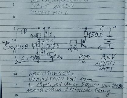
SAFT 14250 SCHALT BILD 150R 150R TLC 555 10k BC212 36V 10u 40n USB 18mA 100ms 1 Minute
in
„Astabiler Multivibrator mit TLC555 (LMC555)“
·
Analoge Elektronik und Schaltungstechnik
·
02.06.2024 23:21
·
Fotos
Bild
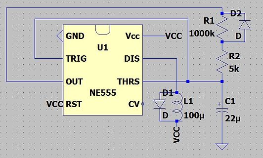
GND Vcc U1 VCC 1000k D2 R1 R2 5k D DIS TRIG THRS OUT CV L1 100µ D1 D VCC 22µ C1 RST VCC
in
„Astabiler Multivibrator mit TLC555 (LMC555)“
·
Analoge Elektronik und Schaltungstechnik
·
06.06.2024 21:51
·
Schaltpläne
Bild
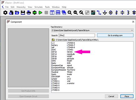
\Local\LTspice\lib\sym\Misc
[..]
battery LT5400-6
cell LT5400-7
DIAC LT5400-8
DIP10 LT5401
DIP14 NE555
DIP16 neonbulb
DIP20 NIGBT
DIP8 PIGBT
Epoly SCR
EuropeanCap signal
EuropeanPolcap tetrode
EuropeanResistor TowTom2
fixedind TRIAC
Gpoly triode
GS61008P urc
jumper urc2
LT5400-1 xtal
LT5400-2
LT5400-
in
„Einschaltverzögerung mitNE555“
·
Analoge Elektronik und Schaltungstechnik
·
21.06.2024 17:11
·
Screenshots
Bild
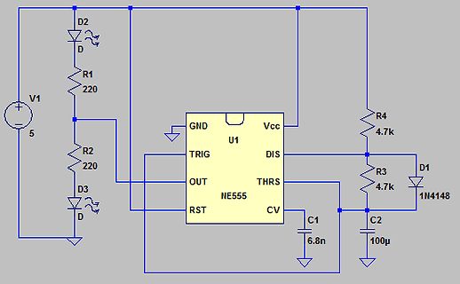
V1 5 R1 220 D2 D R2 220 D3 D U1 GND Vcc TRIG DIS OUT THRS RST CV NE555 R4 4.7k R3 4.7k D1 1N4148 C1 6.8n C2 100µ
in
„NE555 Vergleich Simulation mit Messung“
·
Analoge Elektronik und Schaltungstechnik
·
14.07.2024 11:14
·
Schaltpläne
Bild
555 TIMER
in
„KI Code Generatoren“
·
Offtopic
·
06.10.2024 07:55
·
Fotos
Bild
555 TIMER
in
„KI Code Generatoren“
·
Offtopic
·
06.10.2024 14:01
·
Fotos
Bild
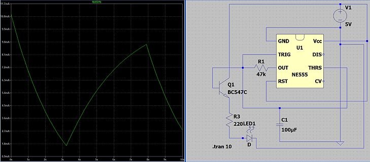
8.1mA 7.2mA 6.3mA 5.4mA 4.5mA 3.6mA 2.7mA 1.8mA 0.9mA 0s 1s 2s 3s 4s 5s 6s 7s 8s 9s 10s V1 5V U1 NE555 GND Vcc TRIG DIS OUT THRS RST CV R1 47k Q1 BC547C R3 220 LED1 C1 100µF D .tran 10
in
„NPN Transistor durch N-MOSFET ersetzen?“
·
Analoge Elektronik und Schaltungstechnik
·
17.03.2025 22:45
·
Screenshots
Bild
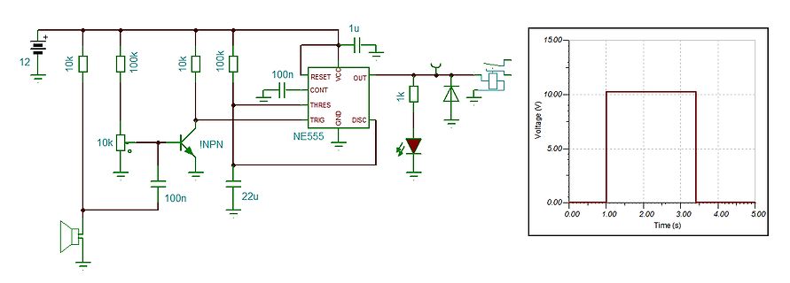
12, 10k, 100k, 10k, 100n, 1u, RESET, VCC, OUT, CONT, THRES, TRIG, GND, DISC, NE555 , 1k, NPN, 100n, 22u, 15.00, 10.00, 5.00, 0.00, Voltage (V), 0.00, 1.00, 2.00, 3.00, 4.00, 5.00, Time (s)
in
„Hilfe bei Umbau Schaltung von Klatschschalter“
·
Analoge Elektronik und Schaltungstechnik
·
18.01.2024 12:58
·
Schaltpläne
Bild
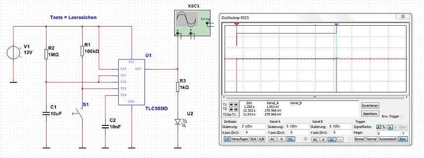
12,303 s T2 bis T1 11,014 s Kanal_A Kanal_B 1,063 V 279,966 mV 279,966 mV V1 12V R2 1MΩ R1 100kΩ U1 TLC555 ID C1 10uF DIS THR TRI CON GND R3 1kΩ C2 10nF U2 V/Div 2 s/Div 5 V/Div Zeitbasis Skalierung X pos. (div) Y pos. (div) Invertieren Speichern Trigger Signalfunktion Pegel Erw. Trigger
in
„Simulation einer NE555 Ausschaltverzögerung in Multisim funktioniert nicht“
·
Analoge Elektronik und Schaltungstechnik
·
27.01.2024 21:27
·
Screenshots
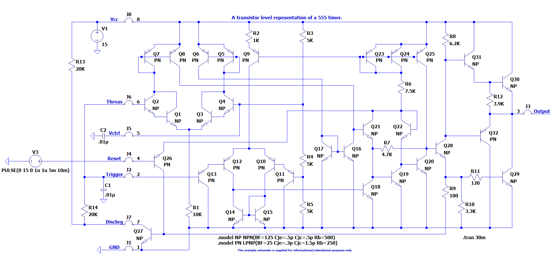
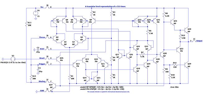
Bild
A transistor level repetaion of a 555 timer.
J8 8
Vcc
R13 20K
Q7 PN
Q8 PN
Q6 PN
R2 1K
Q5 PN
Q9 PN
R3 5K
Q23 PN
Q25 PN
R8 6.2K
Q31 NP
Q2 NP
Q1 NP
Q4 NP
Q21 NP
Q22 NP
R6 7.5K
Q32 PN
J3 Output
R12 3.9K
J6 Thres 6
C2 Vctrl 5
.01u
J5
Reset
Q26
in
„LTspice Schaltplan in Fritzing und Eagle importieren“
·
Analoge Elektronik und Schaltungstechnik
·
18.02.2024 18:16
·
Schaltpläne
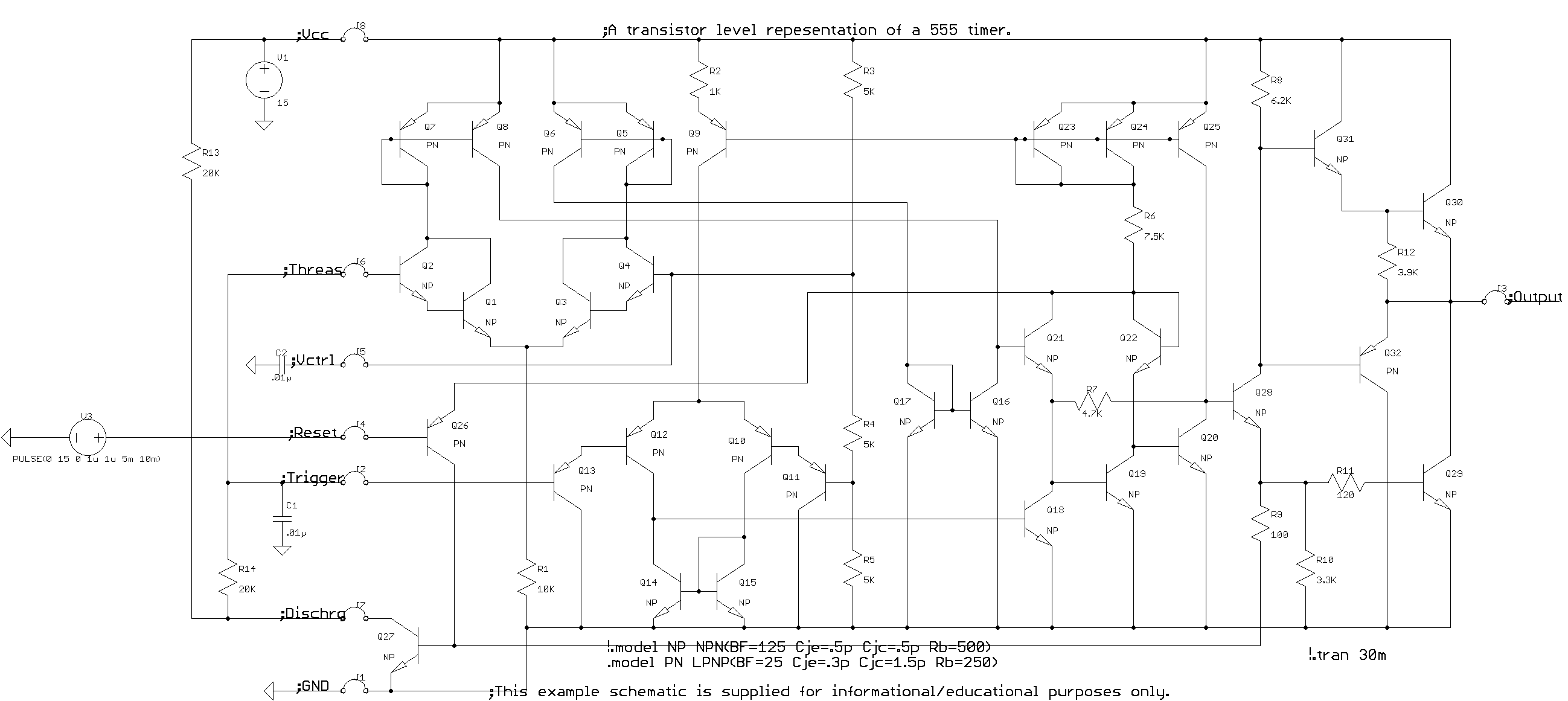
Bild
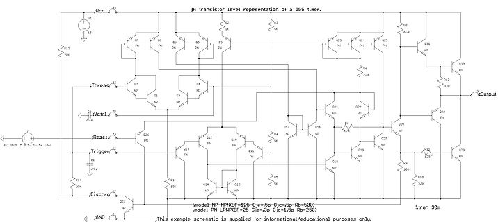
A transistor level repesentation of a 555 timer. U1 Vcc 15 Q7 PN Q8 PN Q6 PN Q5 PN Q2 1K Q9 PN R3 5K Q23 PN Q24 PN Q25 PN R8 6.2K Q31 NP Q30 NP R12 3.9K Output Threas 15 Q2 NP Q1 NP Q3 NP Q4 NP Q21 NP Q22 NP Q7 R6 7.5K Q20 NP Q28 NP Q32 PN
in
„LTspice Schaltplan in Fritzing und Eagle importieren“
·
Analoge Elektronik und Schaltungstechnik
·
18.02.2024 18:17
·
Schaltpläne
Bild
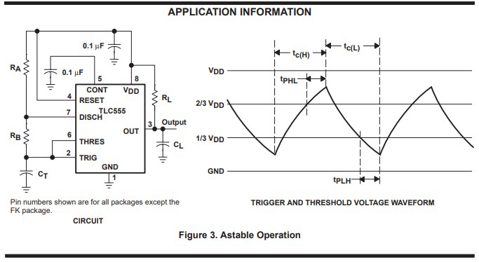
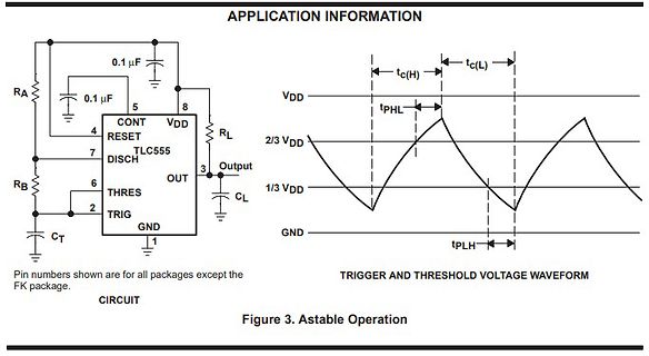
APPLICATION INFORMATION
0.1 µF
0.1 µF
5 CONT
8 VDD
4 RESET
7 DISCH
TLC555
3 Output
6 THRES
2 TRIG
OUT
1 GND
RB
RA
RL
CL
CT
tc(H)
tc(L)
VDD
2/3 VDD
1/3 VDD
GND
tPHL
tPLH
TRIGGER AND THRESHOLD VOLTAGE WAVEFORM
CIRCUIT
Figure 3. Astable Operation
in
„CMOS555 Ausgang3“
·
Digitale Signalverarbeitung / DSP / Machine Learning
·
09.03.2024 11:50
·
Screenshots
Bild
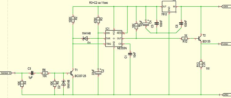
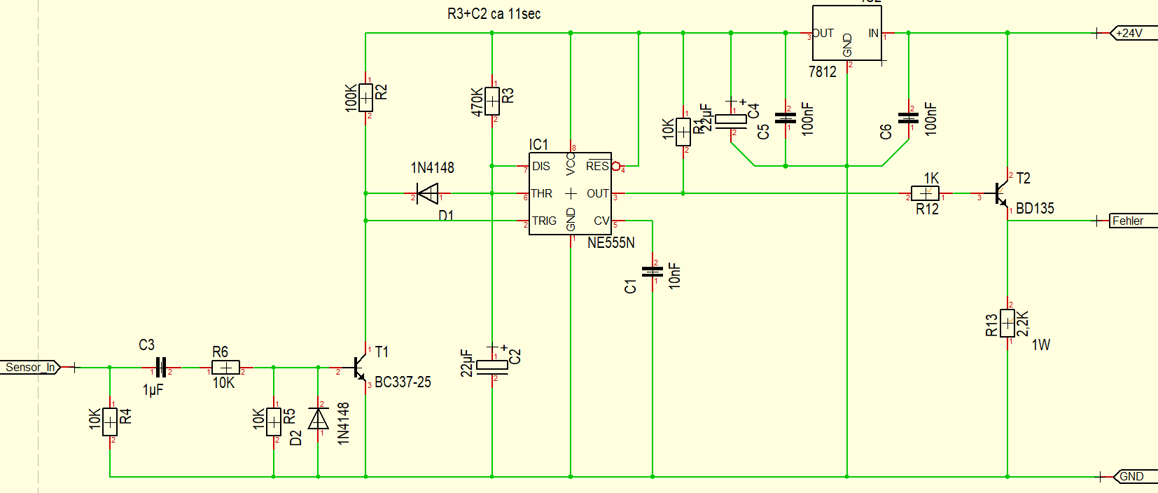
+24V, 10K, 2,2uF, C4, 100nF, C5, 100nF, 1K, T2, BD135, Fehler, R12, 2,2K, 1W, GND, C1, 10nF, CV, NE555 N, C2, 22uF, T1, BC337-25, 1N4148, D2, 10K, R5, 10K, R6, C3, 1uF, Sensor_In, D1, 1N4148
in
„Frage zur Schaltung (Drehüberwachung Zahnrad)“
·
Analoge Elektronik und Schaltungstechnik
·
07.08.2024 10:10
·
Schaltpläne

 Bild
 Bild
 Bild

 Bild

 Bild
 Bild
 Bild
 Bild
 Bild
 Bild
 Bild
 Bild
 Bild
 Bild
 Bild
 Bild
 Bild
 Bild
 Bild
 Bild