Auf http://www.titanmec.com/docc/product-detail-394.html lässt sich das Datenblatt auf chinesisch abrufen. Google-Übersetzer ist Dein Freund ;-) Das Datenformat lässt sich aber auch im Originaldokument anhand der Grafik gut verstehen... Carsten
etwas mit der Timing-Tabelle anfangen? Ist das so zu lesen? T0l (150ns min / 300ns norm / 450ns max) T0h (600ns min / 800ns norm / 1000ns max) T (1200ns min / - norm / - max) TReset (140us min / 500us norm / - max) Gruß Tom
funktionieren und auch für das ADC-Triggersignal. Aber der ADC selbst benutzt einen "normalen" Takt mit max. 60 MHz und mit dem muss der Trigger synchronisiert werden. Für die Abtastzeitpunkte bleibt die Auflösung also bei 16.7 ns. Das sollte aber kein Problem sein, solange du das Signal mit hoher Auflösung
Prescaler auf 1 steht. Dann muss alles noch durch die Matrix und auf den Ausgang. Die Ausgänge können max. 180MHz bei 10pf Last und das mit einer Rise/Fall Time von 1,7ns. Das mit dem Ram wäre kein Problem der Chip hat FSMC und kann externes Ram ansteuern.
Will man vorsichtig sein, reicht es aus nur die betroffenen Signale per set_false_path (oder set_max_delay) zu constrainieren.
MHz. Und einmal durch 116 geteilt. Das ergibt die 8.192 MHz ( = 8.189655172 MHz). Wenn du dir 16.394 MHz erzeugen lässt, dann wird vermutlich durch 58 geteilt, muss aber nicht sein, es könnte auch vorher der Multiplikator verändert werden. Jedenfalls sind deine 8.192 MHz (oder 16.394 MHz) asynchron
uint16_t randstart = 100; uint16_t maxgens = 0; // 2 Spielfelder enum cell_stat feld_last[MAX_X+1][MAX_Y+1]; enum cell_stat feld_next[MAX_X+1][MAX_Y+1]; /* Prüft was mit einer einzelnen Zelle passiert in der nächsten Generation Rückgabe: 0 = lebende Zelle stirbt
Zugriff auf 8 Nachbarn ohne Schleife über ermittelten Offset ptr zeigt auf aktuelles Feld ptr[-MAX_X-1]+ptr[-MAX_X]+ptr[-MAX_X-1] + ptr[-1]+ptr[1] + ptr[ MAX_X-1]+ptr[ MAX_X]+ptr[ MAX_X-1] Ob die Ausgabe wirklich schneller wird, wenn du Änderungen prüfst, sei dahingestellt, hängt vom System
, y a PARTNUMBER/STANDARDCONFIGURATIONS W a Numberof “A” “B” “C” y (10,16) “A” PartNumber Contacts Max. Max. Max. R Max. Max. 1.100 .900 .700 3 514-AG21D 14 (27,49) (22,86) (17,78) 2 . 1.220 1.010 .800 n “C” (2,54) “B” 516-AG21D 16 (30,99) (25,65) (20,32) , Max. Typ. Max. g r e i Note: Before ordering
sollte man wohl eher mit idk 12A rechnen. Ah und ich hab mich vertan, mein 5V Netzteil liefert max 60A ... Also glaube schon, dass mehr als 40A gebraucht werden 🙈
23 14:29:09,168 - ERROR - error flag set ... ending handle_incoming_rpc thread 2024-04-23 14:29:14,394 - ERROR - Exception in RPC thread: tcp connection closed ... 2024-04-23 14:29:14,394 - ERROR - error flag set ... ending handle_incoming_rpc thread 2024-04-23 14:29:19,618 - ERROR - Exception in RPC
UDN2982A, UDN2983A, and UDN2984A Dimensions in Inches (controlling dimensions) 0.014 0.008 18 10 0.430 MAX 0.280 0.300 0.240 BSC 1 9 0.070 0.100 0.005 0.045 0.920 BSC MIN 0.880 0.210 MAX 0.015 0.150 MIN 0.115 0.022 0.014 Dwg. MA-001-18A in Dimensions in Millimeters (for reference only) 0.355 0.204 18 10 10.92 7.11 MAX 7.62 6.10 BSC 1 9 1.77 2.54 0.13 1.15 23.37 BSC MIN 22.35 5.33 MAX 0.39 3.81 MIN 2.93 0.558 0.356 Dwg. MA-001-18A mm NOTES: 1. Exact body and lead configuration at vendor’s option within limits shown
UDN2982A, UDN2983A, and UDN2984A Dimensions in Inches (controlling dimensions) 0.014 0.008 18 10 0.430 MAX 0.280 0.300 0.240 BSC 1 9 0.070 0.100 0.005 0.045 0.920 BSC MIN 0.880 0.210 MAX 0.015 0.150 MIN 0.115 0.022 0.014 Dwg. MA-001-18A in Dimensions in Millimeters (for reference only) 0.355 0.204 18 10 10.92 7.11 MAX 7.62 6.10 BSC 1 9 1.77 2.54 0.13 1.15 23.37 BSC MIN 22.35 5.33 MAX 0.39 3.81 MIN 2.93 0.558 0.356 Dwg. MA-001-18A mm NOTES: 1. Exact body and lead configuration at vendor’s option within limits shown
UDN2982A, UDN2983A, and UDN2984A Dimensions in Inches (controlling dimensions) 0.014 0.008 18 10 0.430 MAX 0.280 0.300 0.240 BSC 1 9 0.070 0.100 0.005 0.045 0.920 BSC MIN 0.880 0.210 MAX 0.015 0.150 MIN 0.115 0.022 0.014 Dwg. MA-001-18A in Dimensions in Millimeters (for reference only) 0.355 0.204 18 10 10.92 7.11 MAX 7.62 6.10 BSC 1 9 1.77 2.54 0.13 1.15 23.37 BSC MIN 22.35 5.33 MAX 0.39 3.81 MIN 2.93 0.558 0.356 Dwg. MA-001-18A mm NOTES: 1. Exact body and lead configuration at vendor’s option within limits shown
rechtlich gleichgestellt sind. Dabei kann man jedes normale Fahrrad mit einem Tretsensor und einem max. 250 Watt Antrieb ausrüsten (ein paar dinge gibts da zu beachten, wie Abschaltkontakte in den Bremsgriffen und max 25 km/h mit elektr. Unterstützung und so) ... sollte aber bei nem guten Set alles dabei
In der KW 25 kostet ein 71 cm Alu-Elektro-Damenfahrrad "nur" 599,00 Euro bei real. (1 cm = 0,394 Zoll)
Verteilung auf die 2 Fühler. Aber es braucht schon ne hinreichend schnelle Abkühlung. Länger als 5, max. 10 Minuten sollte es von 80 auf 50 Grad nicht dauern. Aufheizen von 50 auf 80 Grad in < 1 Minute. Aber da kann man ja vom Widerstand ne Kühlfahne durch die Isolierung legen und nach Tests dann
im Speicher verglichen. Jeweils ein einstellbares Delta für an/aus, aus bei Speicher oder Kollektor max., beide einstellbar. Zusätzlich ist die Pumpe evtl. PWM gesteuert. Da wird es dann komplizierter. Ein Flow Sensor könnte ausgewertet werden für Ertragsanzeige. Für den Betrieb ist das aber nicht
@Gerald: Der Lader ist in dem relvanten Bereich 20-60% auf max. Ladenleistung ausgelegt. Im Mittel ergibt sich zwar eine andere Leistung (Leistungsabgabe und Aufnahme zu Zeit), aber da es der gleiche Balancer ist (bei DC wird er Gleichrichter umgangen) sind es
Powerdip 18 Z 2.54 0.100 16/20 L6201 - L6202 - L6203 mm inch DIM. OUTLINE AND MECHANICAL DATA MIN. TYP. MAX. MIN. TYP. MAX. A 2.35 2.65 0.093 0.104 A1 0.1 0.3 0.004 0.012 B 0.33 0.51 0.013 0.020 C 0.23 0.32 0.009 0.013 D 12.6 13 0.496 0.512 E 7.4 7.6 0.291 0.299 e 1.27 0.050 H 10 10.65 0.394 0.419 h 0.25
Powerdip 18 Z 2.54 0.100 16/20 L6201 - L6202 - L6203 mm inch DIM. OUTLINE AND MECHANICAL DATA MIN. TYP. MAX. MIN. TYP. MAX. A 2.35 2.65 0.093 0.104 A1 0.1 0.3 0.004 0.012 B 0.33 0.51 0.013 0.020 C 0.23 0.32 0.009 0.013 D 12.6 13 0.496 0.512 E 7.4 7.6 0.291 0.299 e 1.27 0.050 H 10 10.65 0.394 0.419 h 0.25
Powerdip 18 Z 2.54 0.100 16/20 L6201 - L6202 - L6203 mm inch DIM. OUTLINE AND MECHANICAL DATA MIN. TYP. MAX. MIN. TYP. MAX. A 2.35 2.65 0.093 0.104 A1 0.1 0.3 0.004 0.012 B 0.33 0.51 0.013 0.020 C 0.23 0.32 0.009 0.013 D 12.6 13 0.496 0.512 E 7.4 7.6 0.291 0.299 e 1.27 0.050 H 10 10.65 0.394 0.419 h 0.25
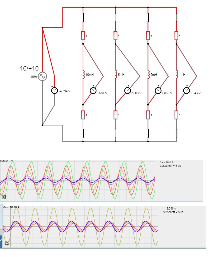
-10/+10 40Hz -4.394 V 1 10mH 1 1.687 V 1 5mH 1 2.803 V 1 2mH 1 1.863 V 1 1mH 1 1.043 V Max=10 V t = 2.698 s Zeitschritt = 5 µs Max=16.48 A t = 2.698 s Zeitschritt = 5 µs
UDN2983A, and UDN2984A Dimensions in Inches (controlling dimensions) 0.014 18 10 0.008 0.430 0.280 MAX 0.240 0BSC0 1 9 0.070 0.100 0.005 0.045 0.920 BSC MIN 0.880 0.210 MAX 0.015 0.150 MIN 0.115 0.022 0.014 Dwg. MA-001-18A in Dimensions in Millimeters (for reference only) 0.355 0.204 18 10 10.92 7.11 MAX 7.62 6.10 BSC 1 9 1.77 2.54 0.13 1.15 23.37 BSC MIN 22.35 5.33 MAX 0.39 3.81 MIN 2.93 0.558 Dwg. MA-001-18A mm 0.356 NOTES: 1. Exact body and lead configuration at vendor’s option within limits shown
UDN2983A, and UDN2984A Dimensions in Inches (controlling dimensions) 0.014 18 10 0.008 0.430 0.280 MAX 0.240 0BSC0 1 9 0.070 0.100 0.005 0.045 0.920 BSC MIN 0.880 0.210 MAX 0.015 0.150 MIN 0.115 0.022 0.014 Dwg. MA-001-18A in Dimensions in Millimeters (for reference only) 0.355 0.204 18 10 10.92 7.11 MAX 7.62 6.10 BSC 1 9 1.77 2.54 0.13 1.15 23.37 BSC MIN 22.35 5.33 MAX 0.39 3.81 MIN 2.93 0.558 Dwg. MA-001-18A mm 0.356 NOTES: 1. Exact body and lead configuration at vendor’s option within limits shown
UDN2983A, and UDN2984A Dimensions in Inches (controlling dimensions) 0.014 18 10 0.008 0.430 0.280 MAX 0.240 0BSC0 1 9 0.070 0.100 0.005 0.045 0.920 BSC MIN 0.880 0.210 MAX 0.015 0.150 MIN 0.115 0.022 0.014 Dwg. MA-001-18A in Dimensions in Millimeters (for reference only) 0.355 0.204 18 10 10.92 7.11 MAX 7.62 6.10 BSC 1 9 1.77 2.54 0.13 1.15 23.37 BSC MIN 22.35 5.33 MAX 0.39 3.81 MIN 2.93 0.558 Dwg. MA-001-18A mm 0.356 NOTES: 1. Exact body and lead configuration at vendor’s option within limits shown
ab. Bereits aufgebaute Vorrichtung Auf dem Bild ist links eine handelsübliche Hysterese-Bremse für max. 20ooo RPM. Rechts befindet sich ein gewöhnlicher Modellbau-Motor als Testobjekt. Dazwischen ist auf den beiden Wellen je ein Flansch mit Mitnehmer montiert. Beide Mitnehmer spannen lastabhängig die
kleinere der beiden mit der Bezeichnung TOR630L hat eine Federkonstante von 0,14 Nmm / °. Sie verträgt max. 394° (ist somit in dem Versuch überdehnt worden). Rechenbeispiel + Drehmoment bei ähnlichen Drehzahlen und unterschiedlich vorgegebener Bremswirkung U/V I/A N/Hz PHI/° M/mNm P/W 0 0 0 0 0 0 10 0.5
30V DC, 10,6x5,5x9mm hoch, Preis ~4Euro Coil Rating, V DC 4.5 Set voltage, V DC (max.) (initial) 3.38 Reset voltage, V DC (max.) (initial) 3.38 Nominal operating current, mA (±10%) 22.2 Coil resistance, Ohm (±10%) 202.5 Nominal operating power, mW 100 Max
effectively without the WITH_UART option. The serial output is normally connected to the input of a MAX323 chip to convert the voltage level to +/- 5V. The input of the MAX232 chip need only low input current. Therefore it is possible, that the input of the MAX323 can be connected to the PC3 pin and
MAX 1 DACs. The resolution will be approximat64 MAX. The interface circuit is a bipolar IC in a DIP16, SO16, or SO20 package made in an I2L-compatible 18 V process.At power-on all DACs are set to their
MAX 1 DACs. The resolution will be approximat64 MAX. The interface circuit is a bipolar IC in a DIP16, SO16, or SO20 package made in an I2L-compatible 18 V process.At power-on all DACs are set to their
16.404ft 10m 32.808ft and background for the spot type is more than 4°C 39.2°F. distance*Remark 1 (Max.) (Max.) (Max.) (Max.) 2. Movement speed • Standard detection type/Spot detection type/ Horizontal*Remark 2 100° 91° 38° 110° • Slight motion detection type: 0.5 m/s DetectionVertical*emark 2 82° 91
16.404ft 10m 32.808ft and background for the spot type is more than 4°C 39.2°F. distance*Remark 1 (Max.) (Max.) (Max.) (Max.) 2. Movement speed • Standard detection type/Spot detection type/ Horizontal*Remark 2 100° 91° 38° 110° • Slight motion detection type: 0.5 m/s DetectionVertical*emark 2 82° 91
16.404ft 10m 32.808ft and background for the spot type is more than 4°C 39.2°F. distance*Remark 1 (Max.) (Max.) (Max.) (Max.) 2. Movement speed • Standard detection type/Spot detection type/ Horizontal*Remark 2 100° 91° 38° 110° • Slight motion detection type: 0.5 m/s DetectionVertical*emark 2 82° 91
Current 0.2 A o Ptot Total Dissipation atcT ≤ 25 C 60 W T stg Storage Temperature -65 to 150 oC o T j Max. Operating Junction Temperature 150 C For PNP types voltage and current values are negative. October 2003 1/4 BDX53F / BDX54F THERMAL DATA R thj-caseThermal Resistance Junction-case Max 2.08 oC/W R thj-amb Thermal Resistance Junction-ambient Max 70 oC/W o ELECTRICAL CHARACTERISTICS (T case= 25 C unless otherwise specified) Symbol Parameter Test Conditions Min. Typ. Max. Unit CEO Collector Cut-off V CE= 80 V 0.5 mA Current (I = 0) E CBO Collector
sieht heftig aus, Gas und Kohle rennen fast am derzeit verfügbaren Limit, Grenzkuppelstellen können max. 20GW (wenn wir den Saft denn überhaupt kriegen), es fehlen aber >21GW. Woher kommt der Rest? Das soll jetzt keine polemisch/politische Diskussion werden was alles gut/richtig oder schlecht/falsch
Hallo H.Joachim S., H.Joachim S. schrieb im Beitrag #7790433: > Grenzkuppelstellen können max. 20GW (wenn wir den Saft denn hast Du dafür eine Quelle? Danke.
abhängig ist? Du bist abhängig von Leistungetransistoren, die schon bei der halben angegebenen max. Verlustleistung durchlegieren? Also die paar ct. für einen Originalhalbleiter hab ich noch.
Reichen dir 55 Tote aufgrund gefälschter Ersatzteile? https://en.wikipedia.org/wiki/Partnair_Flight_394
mmu n eC u re n t Tr a n s f o r me r Dimension PCB Mountable type (unt:mm/i nch) Dimension A(min) B(max) C(max) D(max) E(¡0 .3) F(¡0.3) G(¡0.5) H(¡0¾.3) I TD77V 6.8 25.0 11.0 23.5 15.1 19.1 3.0 9.1 0.268¡¨ 0.984¡¨ 0.433¡¨ 0.925¡¨ 0.594¡¨ 0.752¡¨ 0.118¡¨ 0.358¡¨ TD71V 11.2 28.7 17.0 26.9 15.1 19.1 3.0
Table 10. Display-Test Register Format vers. (Address (Hex) = XF) The example in Figure 2 uses the MAX7219/MAX7221’s segment drivers, a MAX394 single-pole double-throw REGISTER DATA analog switch, and external transistors to drive 2.3” MODE D7 D6 D5 D4 D3 D2 D1 D0 AND2307SLC common-cathode displays.
Table 10. Display-Test Register Format vers. (Address (Hex) = XF) The example in Figure 2 uses the MAX7219/MAX7221’s segment drivers, a MAX394 single-pole double-throw REGISTER DATA analog switch, and external transistors to drive 2.3” MODE D7 D6 D5 D4 D3 D2 D1 D0 AND2307SLC common-cathode displays.
Table 10. Display-Test Register Format vers. (Address (Hex) = XF) The example in Figure 2 uses the MAX7219/MAX7221’s segment drivers, a MAX394 single-pole double-throw REGISTER DATA analog switch, and external transistors to drive 2.3” MODE D7 D6 D5 D4 D3 D2 D1 D0 AND2307SLC common-cathode displays.
Table 10. Display-Test Register Format vers. (Address (Hex) = XF) The example in Figure 2 uses the MAX7219/MAX7221’s segment drivers, a MAX394 single-pole double-throw REGISTER DATA analog switch, and external transistors to drive 2.3” MODE D7 D6 D5 D4 D3 D2 D1 D0 AND2307SLC common-cathode displays.
Table 10. Display-Test Register Format vers. (Address (Hex) = XF) The example in Figure 2 uses the MAX7219/MAX7221’s segment drivers, a MAX394 single-pole double-throw REGISTER DATA analog switch, and external transistors to drive 2.3” MODE D7 D6 D5 D4 D3 D2 D1 D0 AND2307SLC common-cathode displays.
Table 10. Display-Test Register Format vers. (Address (Hex) = XF) The example in Figure 2 uses the MAX7219/MAX7221’s segment drivers, a MAX394 single-pole double-throw REGISTER DATA analog switch, and external transistors to drive 2.3” MODE D7 D6 D5 D4 D3 D2 D1 D0 AND2307SLC common-cathode displays.
Table 10. Display-Test Register Format vers. (Address (Hex) = XF) The example in Figure 2 uses the MAX7219/MAX7221’s segment drivers, a MAX394 single-pole double-throw REGISTER DATA analog switch, and external transistors to drive 2.3” MODE D7 D6 D5 D4 D3 D2 D1 D0 AND2307SLC common-cathode displays.
Table 10. Display-Test Register Format vers. (Address (Hex) = XF) The example in Figure 2 uses the MAX7219/MAX7221’s segment drivers, a MAX394 single-pole double-throw REGISTER DATA analog switch, and external transistors to drive 2.3” MODE D7 D6 D5 D4 D3 D2 D1 D0 AND2307SLC common-cathode displays.
Table 10. Display-Test Register Format vers. (Address (Hex) = XF) The example in Figure 2 uses the MAX7219/MAX7221’s segment drivers, a MAX394 single-pole double-throw REGISTER DATA analog switch, and external transistors to drive 2.3” MODE D7 D6 D5 D4 D3 D2 D1 D0 AND2307SLC common-cathode displays.
otherwise noted, the following specifications apply= +3.0V to +5.5V with T = T to T , C to CC AMB MIN MAX 1 C 40.1µF PARAMETER MIN. TYP. MAX. UNITS CONDITIONS DC CHARACTERISTICS Supply Current 0.3 1.0 mA no load, TAMB = +25°C, VCC = 3.3V, TxIN = V or GND CC Shutdown Supply Current 1.0 10 µA SHDN = GND,

 Bild
Bild