Parallel (default) Noritake Sales Office Tel Nos L H 46H = Fill Area Link Serial Nagoya Japan: +81 (0)52-561-9867 L H 43H = Clear Area Canada: +1-416-291-2946 L H 4FH = Set Outline Box SERIAL MODE Chicago USA: +1-847-439-9020 L H 6FH = Clear Outline Bo J9 J10 Configuration Munchen (D): +49 (0)89-3214-290
voltage at a given output T N C voltage, which needs to be a minimum of 1.43 times the output ISHARE S G V PGND1 voltage if operating at F = 700kHz switching frequency. This is I P P SW PVCC= IN due to the Minimum
Ben S. schrieb im Beitrag #6290174: > Eine neuste Studie ergibt: Man sollte seine Alltagsmasken auch zu Hause > tragen: > > https://www.msn.com/de-at/lifestyle/other/laut-einer-studie-sollte-man-schutzmasken-auch-zu-hause-tragen
A. K. schrieb im Beitrag #6296282: > Ben S. schrieb im Beitrag #6296271: >> Eben, normalerweise hätte das hierzulande niemanden groß interessiert. > > Es kommt noch ein wenig Trump hinzu. Was vor dem Hintergrund von https://www.wochenblick.at
compatible with ST16C554D, and software compatible with ST16C454/554, ST16C554, TL16C554 ■ Up to 5 Mbit/s data rate at 5 V and 3.3 V, and 3 Mbit/s at 2.5 V ■ 5 V tolerant inputs ■ 16-byte transmit FIFO ■ 16-byte receive FIFO with error flags ■ Programmable auto- RTS and auto-CTS In auto-CTS mode, CTS controls
when used in a controlled environment. Maintaining ambient temperature of between 22–28 °C [72-82 °F] at a relative humidity of 40–60% will ensure consistent performance and maximum life of paste. Do not let the print temperature exceed 32 °C [89 °F]. Cleaning Misprint Boards In case of a misprinted board
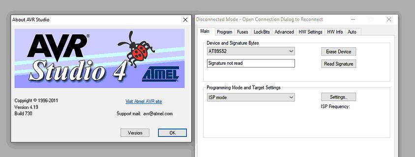
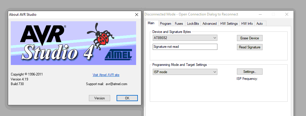
Reconnect
Main Program Fuses LockBits Advanced HW Settings HW Info Auto
Device and Signature Bytes
AT89S52
Erase Device
Signature not read
Read Signature
Programming Mode and Target Settings
ISP mode
Settings..
ISP Frequency:
Kauf dir ein Balkonkraftwerk mit Speicher und Inselbetrieb und/oder einer "Notstrom-Steckdose". Gibt's doch inzwischen alles preiswert von zig Anbietern
Wasser aus > der Dusche kommt. Da habe ich schon seit Jahrzehnten eine einfache Steuerung mit AT89C2051 vorgesehen. 1 x drücken: 10 Minuten Betrieb; 3 x 1 h; 4 x 2 h und 5 x wieder ausschalten. Bei den längeren Perioden wird sie alle 10 Minuten für 1 Minute eingeschaltet. Das funktioniert im Sommer
300567 Und es gibt noch "The Standard C Library" von P.J. Plauger. Das bezieht sich zwar auf C89, dafür aber mit Kommentaren und Quellcode zu den Standardfunktionen. Plauger hat C89 selber mit verabschiedet.
selbst bekannt. Das ist bei Pascal durchaus anders, dort sind Funktionen wie chr, val, inc, dec, write, at usw. im Sprachumfang enthalten, weswegen der Pascal-Compiler sowas ohne jegliche uses Anweisung von sich aus kennt. Also, Rolf, hast du das nun verstanden? W.S.
Langeweile? Ich war früher auch mal militanter float Gegner, hab dann aber gemerkt, daß selbst ein AT89C51 @12MHz reichlich Power hat, damit der Benutzer nicht die geringsten Laufzeitunterschiede merkt. Ich benutze inzwischen auch ausschließlich sprintf, sscanf, statt mir umständlich was selber zu basteln
Mangoldt, Knopp, Höhere Mathematik 1, Hirzel Verlag, 1990 64. Endliche regelmäßige Kettenbrüche S. 144 65. Näherungsbrüche S. 147 66. Beispiele S. 149
set the toler- ance on the simulator for solving equations. As an steps allowing for a better chance at converging example, in IC’s the current can be in µA, but if • Check the “Use GMIN stepping to improve con- simulating a switching power supply the currents vergence” option if its available. This will
E T 3 low-order Class-E circuit will work 4 1 3 F F E E T F E 3 well with a particular transistor at fre- F F T 8 S S S F F E S c quencies up to about 17%/25% = 70% I I F R E E E E S M E e of the frequency at which that transis- r r S M sM s M M E 4 M f T i i O s A A A 1 M - P e tor works well in a
> Die H8, H8S, H8SX, SHxx und RX wirken dagegen homogen. > Ignorieren will ich aber auch nicht, dass die diversen ARMe/Cortexe > deutlich kostengünstiger erscheinen. Bei meinen Stückzahlen ist mir das > allerdings
sage ich dir welchen Mikrocontroller ich 2015 verwenden werde. Im Moment arbeite ich viel mit dem AT89S52, ein zuverlässiges Arbeitspferd mit ISP, aber keinerlei besonderen Features. Ich werde wohl in Zukunft auf SILABS umsteigen. Die niedrige Versorgungsspannung ist für gemischt analog digitale Systeme
(PSRR) is defined as the The measured ratio of signal-to-(noise + distortion) at the ratio of the power in the ADC output at full-scale frequency, f, output of the ADC. The signal is the rms amplitude of the to the power of a 100 mV p-p sine wave applied to the ADC’s fundamental.
corrections, modifications or improvements, to this document, and the products and services described herein at any time, without notice. All ST products are sold pursuant to ST’s terms and conditions of sale. Purchasers are solely responsible for the choice, selection and use of the ST products and services described
02/20/2022 IS25LP128 3. BLOCK DIAGRAM C o tolLogi HighV olageG enertor Sttus IO Bufersand Registr D at Lathes C E# 256B yes Page Bufer e SC K c r t W P# l (O2) r Y - ec der h SI r (O0) e l SO r (O1) S (1) HO LD# orRES ET# r (IO3) d o e M emoryArray - X A ddrss Lath & Counter Note1: For RESET# pin option
/24 – 0.5 The fact that the fractional Julian Date may be negative is OK. 1 By definition, the sun’s shadow falls along a north-south meridian at local solar noon (not local clock noon), which can be found using online solar position calculators. See, for example, http://www.instesre.org/Solar/insolation.htm
C Figure 5 Pulse Width Modulation Soft-StartIn case the amplified current sense signal exceeds the at pin SoftS. Thus it is ensured that at every switch-on the voltage ramp at pin SoftS starts at zero. FB signal the on-time T on of the driver is finished by reseting the PWM-Latch (see Figure 5). Version
Fig 1. Typical Output Characteristics Fig 2. Typical Output Characteristics 1000 2.0 D = 15A c ) n ( s n s e e 1.5 u TJ= 25 C R C O ) e e ed r ° r l o100 TJ= 150 C o a1.0 - S r t t o i n ( r a D D , , 0.5 ID n ( V DS = 15V S 20µs PULSE WIDTH R VGS =10V 10 0.0 2.0 3.0 4.0 5.0 6.0 7.0 -60 -40 -20 0 20 40
COC2 6 PIP005 5 1 PIP001 COC2 6 SH2 2HS0eludoMetupmoCIP 1 +1.8 Header 3X2A+1.8 1 SHIELD P1 u P4 u S S S S S S S S S S S S S S S S S S S S S S S S S S S S S S S S S S S S S S S S S S S S S S S S S S S S S S S S S S S S S 1 1 V V V V V V V V V V V V V V V V V V V V V V V V V V V V V V V V V V V V V V
solchiges Arduino R3 Format "zurechtzustutzen" Einmal für STM32F030F4P6 uuuund einmal für AT89S52 PLC44 (MCS-51 Familie) Den STM32 hab ich mir nur besorgt gehabt um zu sehen, was man denn mit einem 32-Bitter mit nur 16Kb Flash anfangen kann und ich bin erstaunt. Erstens geht man (zunächst
: 335S0665 1 32GB SAMSUNG 35NM FLASH TLGA52 U1 Y BETTER_MURATA T A B L E _ 5 _ I T E M T A B L E _ A L T _ I T E M335S0707 1 64GB SAMSUNG 35NM FLASH LGA52 U1 Y BEST_MURATA NIMBUS, GRAPE, LCD CONN. 197S0334
QUAD OPERATIONAL AMPLIFIERS SLOS092D – SEPTEMBER 1987 – REVISED MARCH 2001 electrical characteristics at specified free-air temperature, V DD = 10 V (unless otherwise noted) TLC274I, TLC274AI, PARAMETER TEST CONDITIONS TA † TLC274BI, TLC279I UNIT MIN TYP MAX 25°C 1.1 10 TLC274I V O = 1.4 V, VIC= 0, R S
self-timed Write operation completed, poll the WIP bit. Integrated Silicon Solution, Inc.- www.issi.com 52 Rev. L6 04/15/2019 IS25LP128 Table 8.3 Instructions accepted during Suspend Operation Instruction Allowed Suspended Name Hex Code Operation Program or Erase NORD 03h Read Data Bytes from Memory at Normal
erlaubt es, jeweils zwischen 59 Sekunden- 1 Sekunde aus bzw. Einzeit mittles Taster zu wählen. Ist mit AT90s2313 bestückt. Bei Bedarf schicke ich den Bascom Code per E-Mail. MfG Paul
deswegen habe ich den Wiederstand experimentell soweit verringert. Man kann selbstverständlich das S202T02 auch gegen ein S26MD02 austauschen, da ich die T02 version aber liegen hatte, habe ich diese verwendet. Das Board habe ich für den T02 und S02 ausgelegt. Du kannst auch vom Typ S202S02 2 Stück
gab, wo eine Schaltung jahrelang in Massenproduktion funktionierte, bis einer von den VCC-Pins am AT90S8535 auf mehreren Platinen nicht gelötet war. Der Fehler beim E-Test war Kurios: Die Digital-Logik am anderen Ende des Controllers ging nicht... Es war garkeine VCC an den Pads zu messen. Nach
AVR --> Studio 4 + ASM ODER WinAvr, noch kein "Inline ASM" gemacht. 8051 --> SDCC (AT89S52 PLCC44 - Die lagen Stangenweise rum - macht aber wenig Spaß, weil der aus Studio 4 bald 2 Minuten flasht.) S12/HC12 --> Frescale CodeWarrior. (Alles z.B. für Testaufbauten in der Firma.)
// FIRMWARE REPLACEMENT FOR CHATPAD's pic16f883 // see attached documents to learn more // release 0.3.1 from jean : giancarlotodone at yahoo dot it // for the Open Keyboard Project // thanks alot to Gidi (who owns an half of my chatpad,
0.41 K 0.695 0.725 17.65 18.42 B L 0.290 0.300 7.37 7.62 N 0.420 0.440 10.67 11.18 P 0.153 0.159 3.89 4.04 Q 0.153 0.159 3.89 4.04 1 2 3 4 5 6 K R 0.230 0.250 5.84 6.35 S 0.220 0.240 5.59 6.10 PIN 1 S U 0.910BSC 23.11BSC V 0.182 0.194 4.62 4.93 C –P– G D 6 PL 0.25(0.010) M T Q M STYLE1: J F 0.13(0.005
that we are guaranteeing the product as “unbreakable.” Code protection is constantly evolving. We at Microchip are committed to continuously improving the code protection features of our products. Attempts to break Microchip’s code protection feature may be a violation of the Digital Millennium Copyright
size of the required adjust pin capacitor is a function of the input ripple frequency. If R1=100Ω at 120Hz the not be exceeded under continuous normal load conditions. adjust pin capacitor should be >13µF. At 10kHz only 0.16µF is Careful consideration must be given to all sources of thermal resistance
SOLDERING REFLOW (Note 2) Lead Temperature Soldering T °C SLD Reflow (SMD styles only), Leaded, 60−150 s above 183, 30 s max at peak − 240 Reflow (SMD styles only), Lead Free, 60−150 s above 217, 40 s max at peak − 265 Wave Solder (through hole styles only), 12 sec max − 310 2. Per IPC/JEDEC J−STD−020C.
this thesis. Figure 15 illustrates the current and voltage values used for the computation of Rdc,10s 𝑅dc,10s= 𝑉10s−𝑉0s = 𝑉10s−𝑉0s for 𝐼0s = 0 A (5) pulse−0s pulse Since the dynamic behavior of battery cells depends strongly on temperature, the resistance measurements have to be performed at controlled
N TA= 25°C ( 67 E 66 Radj= Open T 66 R 64 E TA= 25°C U R 65 Radj= Open C 62 R 64 E C 63 A 60 E 62 S S Y 58 U 61 D P 60 E 56 P 59 T g , 54 I 58 Non−Repetitive Pulse Test S 57 g 52 56 I 50 3.0 4.0 5.0 6.0 7.0 8.0 9.0 10 54 56 58 60 62 64 66 68 70 72 74 76 78 Vak, ANODE−CATHODE VOLTAGE (V) reg(P)PULSE
D9. 1/4 3 P l 2V 1 W e g 2 1 2 1 2 1 i 2U M 1V p t D31. 1/1 11 D71. 1/1 31 D71. 1/1 11 k 2 W ~3 1U at E N 3 2 1 e n D61. 1/1 31 P L L L r o 1 M e r WK01 h ü r f dnabr edr öF GNUSI EPSNI E e ch H P i 89 79 d r zt euhcskcei er D zt euhcszt eN zt euhcsnr et S n e 69 59 u B B31. 1/ : e mani et aD.r N-skr
Information XC62Hxxxxxxx a b c d e f DESIGNATOR DESCRIPTION DESIGNATOR DESCRIPTION TrueLogic Level at CEPin: a R=Positive PackageType P=Negative(Custom) e M=SOT-25 P=SOT-89-5 Output Voltage b 30=3.0V 50=5.0V DeviceOrientation 0 c R=EmbossedTape f (Orientationof Device:Right) L=EmbossedTape Output VoltageAccuracy

 Bild
Bild