-
Datei
oscilloscopeV6.html
"> <label>Phase: <input id="phase" type="range" min="0" max="6.28" step="0.1" value="1.57"> <span id="phaseVal">1.57</span></label> <label>Speed: <input id="speed" type="range" min="1" max="100" step="1" value="10"> <span id="speedVal">10</span></label> </div> <div id="controls"> <label>Path Length: <input id="pathLength" type="range" min="1" max="500" step="10" value="100"> <span id="pathVal">100</span></label> </div> <canvas id="scope" width="600" height="500"></canvas> <br> 2025-01-27 mchris with the help of Perplexity <script> const canvas
-
PDF
datasheet.pdf
Voltage -0.3 to +32 V Vid Differential Input Voltage - (*) +32 +32 +32 V Ptot Power Dissipation N Suffix 500 500 500 mW D Suffix - 400 400 mW - Output Short-circuit Duration - (note 1) Infinite in Input Current – (note 6) 50 50 50 mA o T oper Operating Free Air Temperature Range -55 to +125 -40 to +105 0 to
in „LM324 - Versorgungsspannung“ · Mikrocontroller und Digitale Elektronik ·
-
 Bild
Ausschnitt aus einem Datenblatt mit Tabelle und Leiterplatten-Layout
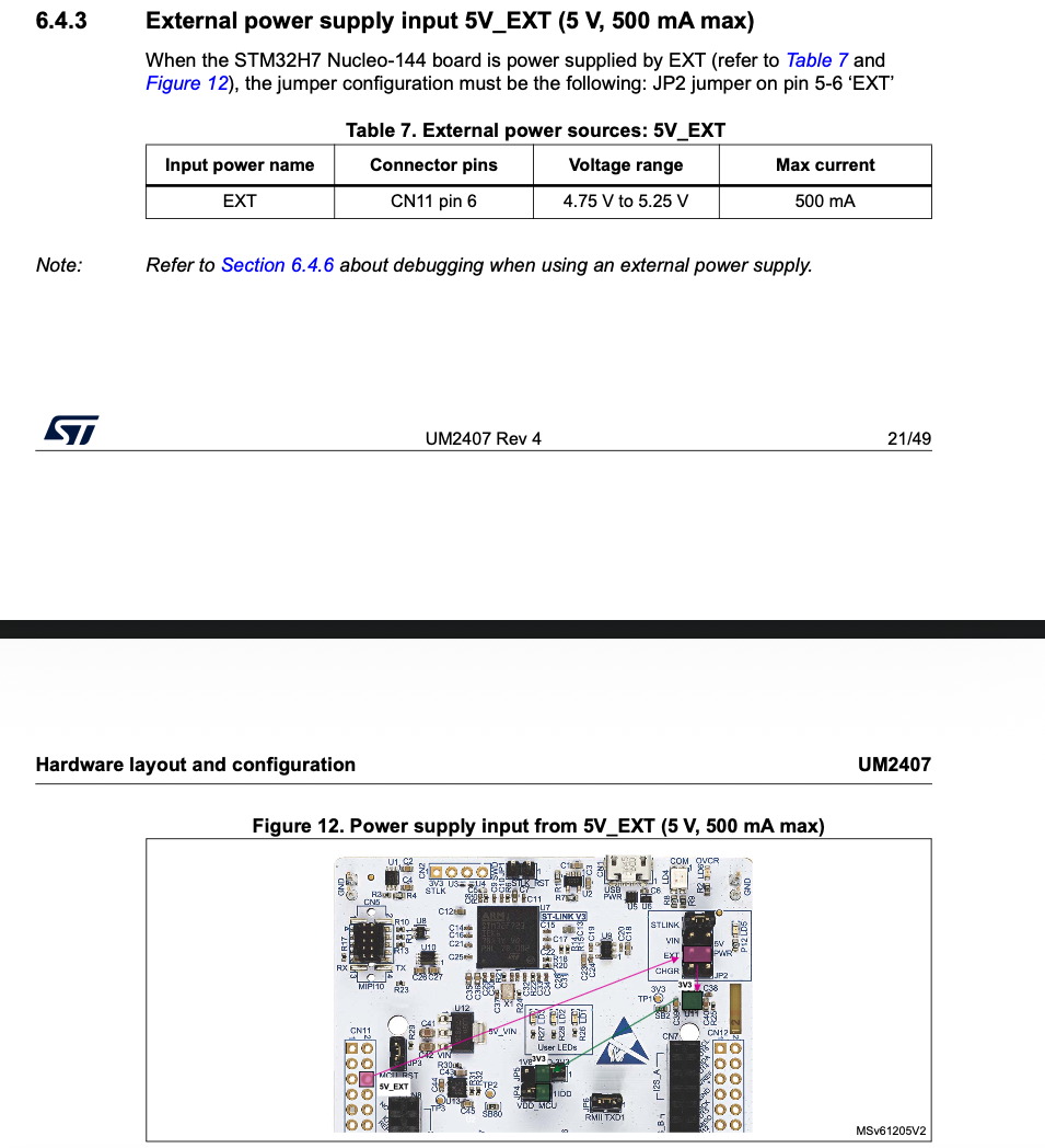
6.4.3 External power supply input 5V_EXT (5 V, 500 mA max) When the STM32H7 Nucleo-144 board is power supplied by EXT (refer to Table 7 and Figure 12), the jumper configuration must be the following: JP2 jumper on pin 5-6 'EXT' Table 7. External power sources: 5V_EXT EXT CN11 pin 6 4.75 V to 5.25 V 500 mA Note: Refer to Section 6.4.6 about debugging when using an external power supply. UM2407 Rev 4 21/49 Hardware layout and configuration Figure 12. Power supply input from 5V_EXT (5 V, 500 mA max)
in „L7805 überhitzt bei bestimmten Last-Szenarien“ · Analoge Elektronik und Schaltungstechnik · · Screenshots
-
PDF
AD538_c.pdf
VS= 615 V, T A +258C unless otherwise noted) AD538AD AD538BD AD538SD Parameters Conditions Min Typ Max Min Typ Max Min Typ Max Units MULTIPLIER DIVIDER PERFORMANCE Nominal Transfer Function m m m VZ VZ V Z 10 V V X VY, Z 0 VO= V Y ÷ VO= Vy ÷ V O V Y ÷ VX VX V X m m m IZ IZ IZ 400 A IX, Y,Z 0 VO= 25 k
in „Wurzeloperation mit Operationsverstärker“ · Analoge Elektronik und Schaltungstechnik ·
-
PDF
AD538_analog_rechnen.pdf
VS= 615 V, T A +258C unless otherwise noted) AD538AD AD538BD AD538SD Parameters Conditions Min Typ Max Min Typ Max Min Typ Max Units MULTIPLIER DIVIDER PERFORMANCE Nominal Transfer Function m m m VZ VZ V Z 10 V V X VY, Z 0 VO= V Y ÷ VO= Vy ÷ V O V Y ÷ VX VX V X m m m IZ IZ IZ 400 A IX, Y,Z 0 VO= 25 k
in „Beschaltung eines analogen Positionssensors“ · Analoge Elektronik und Schaltungstechnik ·
-
PDF
AD538_analog_rechnen.pdf
VS= 615 V, T A +258C unless otherwise noted) AD538AD AD538BD AD538SD Parameters Conditions Min Typ Max Min Typ Max Min Typ Max Units MULTIPLIER DIVIDER PERFORMANCE Nominal Transfer Function m m m VZ VZ V Z 10 V V X VY, Z 0 VO= V Y ÷ VO= Vy ÷ V O V Y ÷ VX VX V X m m m IZ IZ IZ 400 A IX, Y,Z 0 VO= 25 k
in „Zu viel Rauschen bei OPV Schaltung“ · Analoge Elektronik und Schaltungstechnik ·
-
PDF
start-booster-und-start-truck.pdf
Gartengeräte etc. · Spannungsspitzenschutz Technische Daten: START BOOSTER 1000 START BOOSTER 1600 Max. Stromstärke (Spitzenleistung) 1000 A 1600 A Innenbatterie 12 V / 17 Ah 12 V / 16 Ah I-Start 300 A 600 A Ladespannung max. 14,9 V 14,9 V Lebensdauer 550 Zyklen (bei 52%iger Entladung) 500 Zyklen (bei
in „Auto mit kleinem Bleigelakku starten/anlassen?“ · Offtopic ·
-
PDF
3703fc.pdf
thatthemaximumvoltagedifferencebetweenDRV CC and PROG BGRTNis15V.If,forexample,V BGRTN =–2V,themaximum 500mV. Values outside of this range may give less accu- voltage on DRV pin is now 13V instead of 15V. rate current limit. The current limit can also be disabled CC by floating theMAX pin. Current Limit
in „Längs- oder Querregler 40V 250W als Überspannungsschutz für Tiefstellsetzer“ · Analoge Elektronik und Schaltungstechnik ·
-
PDF
155762-da-01-en-LOGIK_IC_M74HC595B1R_STM.pdf
Temperature -55 to 125 °C Input Rise and Fall Time V = 2.0V CC 0 to 1000 ns tr ft VCC = 4.5V 0 to 500 ns VCC = 6.0V 0 to 400 ns 4/16 M74HC595 DC SPECIFICATIONS Test Condition Value T = 25°C Symbol Parameter VCC A -40 to 85°C -55 to 125°C Unit (V) Min. Typ. Max. Min. Max. Min. Max. VIH High Level Input
in „uC + 3 Schieberegister + 7-Segmentanzeige“ · Mikrocontroller und Digitale Elektronik ·
-
PDF
rd.pdf
2.0 2.5 3.5 5.0 5.0 7.5 7.5 10.0 12.5 . P 0.5 0 d 0.5 0.5 0.6 0.6 0.6 0.8 0.8 1.0 1.0 D 0.5 1.0 L max. 15 min. 4 min. 1.5 2.0 Safety ve6.3 up) 55 MINIATURE ALUMINUM ELECTROLYTIC CAPACITORS series DIMENSIONS & MAXIMUM PERMISSIBLE RIPPLE CURRENT WV 6.3 10 16 25 35 50 63 100 160 200 250 350 400 450 500
-
PDF
ADJ11005_to_ADJ24048.pdf
Contact Characteristics Arrangement 1 Form A, 1 Form C Initial insulation resistance* Min. 1,000 M (at 500 V DC) Initial contact resistance, max. 100 m Initial Between open 1,000 Vrms for 1 min. (By voltage drop 6 V DC 1 A) contacts Contact material Silver alloy breakdown3 Between contacts and voltage* coil 4,000 Vrms for 1 min. Nominal switching capacity 16 A 250V AC Max. switching power 4,000 V A Surge voltage between contact and Rating coil*4 Min. 10,000 V (initial) (resistive load) Max. switching voltage 250V AC 5 Max. switching current 16 A Set time* Approx. 10ms
-
PDF
Hameg_Encoder_ALPS-EC11J.pdf
Shaft At R=5kΩ At R = 5kΩ At R = 5kΩ Ring Chattering: 5msmax. Chattering :2ms max. Chattering :3ms max. Type Bounce: 2msmax. Bounce :2ms max. Bounce :2ms max. EC11EH EC20A EC11J/EC11K Test circuit ▯7▯%$ V1=V 2=2.5V max. 3 3 3 Test circuit Output waveform 5FSNJOBM▯" 5FSNJOBM▯# 5FSNJOBM
-
PDF
BCAP0025P300X12_3V_25F.pdf
IPEAK Peak Current BOL, Note 4,8 – – 24 A BOL, Note 7,8 I Continuous Current - ∆T = 15°C – – 4.4 A MAX RMS - ∆T = 40°C – – 7.2 LIFE VR= 3V and TA= 65°C, EOL, Note 8 – 2,000 – hours t High Temperature Life - Capacitance change ΔC from min C – -20 – % 65C - Resistance change ΔR from max R R – +100 – % S V = 2.7V and T = 85°C, EOL, Note 8 – 1,500 – hours t De-rated Voltage & Higher - Capacitance change ΔC from min C – -20 – % 85C Temperature Life R - Resistance change ΔR from max RS – +100 – % V = 3V and T = 25°C, EOL, Note 8 – 10 – years R
-
Datei
mmc.c
Commando an die MMC/SD-Karte u8 mmc_write_command (u8 *cmd){ u8 a; u8 tmp ; u16 Timeout = 0,b; tw_set(2,500);//500ms do{ tmp=mmc_read_byte (); }while(tmp==0x0 && (tw_read(2)!=0));//wartet max.500ms bis nicht mehr busy mmc_write_byte(*cmd++); mmc_write_byte(*cmd++); mmc_write_byte(*cmd++); mmc_write_byte(*
in „MMC SD library FAT16 FAT32 read write“ · Projekte & Code ·
-
PDF
LED_Leuchtmittel.pdf
in solch einem Abstand von der Leuchte das 500 Lux erreicht werden (z.B. Straßenbeleuchtung) durchgeführt. ▯ Über die 500 Lux Methode besteht auf jeden Fall noch Klärungsbedarf. Was passiert bei solchen Leuchten mit dem Personal, das Reinigungs-
in „Personenschutz an LED Lampen“ · Analoge Elektronik und Schaltungstechnik ·
-
PDF
mcr22.pdf
Number: May, 2000 – Rev. 3 MCR22–6/D MCR22–6, MCR22–8 THERMAL CHARACTERISTICS Characteristic Symbol Max Unit Thermal Resistance, Junction to Case R 50 ⋅C/W θJC Thermal Resistance, Junction to Ambient R 160 ⋅C/W θJA Lead Solder Temperature TL +260 ⋅C (Lead Length q 1/16 from case, 10 s Max) ELECTRICAL
in „TV: Bauteil ?? MCR22-8“ · Mikrocontroller und Digitale Elektronik ·
-
PDF
MC34064.pdf
ESD data available upon request. ELECTRICAL CHARACTERISTICS (For typical valueA T = 25⋅C, for min/max valueA T is the operating ambient temperature range that applies [Notes 2 and 3] unless otherwise noted.) Characteristics Symbol Min Typ Max Unit COMPARATOR Threshold Voltage V High State Output (inIncreasing
in „Spannungsmonitor mit zweifarbiger LED“ · Analoge Elektronik und Schaltungstechnik ·
-
PDF
Bluetooth-Modul_PAN1x55__BlueMod_P2xG2__Test-Report-1097464.pdf.pdf
described in detail in the Annex of the testreport Conducted measurements are valid for both types Max. power radiated: 4.5 dBm EIRP (GFSK) internal antenna Max. power radiated: 7.9 dBm EIRP (GFSK) external antenna Max. power conducted: 4.9 dBm (GFSK) FCC ID: T7V-BC06 IC: 216Q-BC06 2009-03-11 Page 6
in „Bluetooth-Modul "BlueMod+P25" von Stollmann - Ersatztyp“ · Mikrocontroller und Digitale Elektronik ·
-
PDF
AD811.pdf
Intercept @ C = 10 MHz ±15 36 36 dBm ±15 43 43 dBm INPUT OFFSET VOLTAGE ±5 V, ±15 V 0.5 3 0.5 3 mV TMINto MAX 5 5 mV Offset Voltage Drift 5 5 µV/°C INPUT BIAS CURRENT −Input ±5 V, ±15 V 2 5 2 5 µA TMINto MAX 15 30 µA +Input ±5 V, ±1 5 V 2 10 2 10 µA TMINto MAX 20 25 µA TRANSRESISTANCE TMINto MAX VOUT= ±10 V
in „2 Spannungen in einer Schaltung“ · Analoge Elektronik und Schaltungstechnik ·
-
PDF
dvm13mfc2.pdf
0.01Hz to 100Hz AC couple 100Hz to 50MHz Sensitivity AC: 100Hz ~ 50MHz < 80m Vrms DC: 0.01Hz ~ 1Hz ≤ 500m Vp-p 1Hz ~ 100Hz ≤ 80m Vrms Impedance 1 Mohms Attenuator X1, X20 Max. Safety Voltage 30V (DC/AC peak) Channel B (50MHz ~ 2.4GHz) Frequency Range from 50MHz to 2.4GHz Sensitivity 50MHz ~ 1.2GHz ≤ 50m
in „Was taugt dieser Frequenzzähler“ · Analoge Elektronik und Schaltungstechnik ·
-
PDF
ad7328.pdf
20 MHz max tCONVERT 16 × tSCLK 16 × tSCLK ns max tSCLK= 1/fSCLK t 75 60 ns min Minimum time between end of serial read and next falling edge of CS QUIET t1 12 5 ns min Minimum CS pulse width t22 25 20 ns min CS
in „was bringt ADC mit Sequencer (AD7328)?“ · Mikrocontroller und Digitale Elektronik ·
-
PDF
61C256AH.pdf
SUPPLY CHARACTERISTICS (Over Operating Range) -10 -12 -15 -20 Symbol Parameter TestConditions Min. Max. Min. Max. Min. Max. Min. Max. Unit ICC VccDynamicOperatingC=Max.,CE=VIL Com. — 165 — 155 — 145 — 135 mA SupplyCurrent OUT=0mA,f=fMAX Ind. — — — 165 — 155 — 145 IS1 TTLStandbyCurrent VC=Max., Com. —
in „Write cycle SRAM“ · Mikrocontroller und Digitale Elektronik ·
-
PDF
SN75512b.pdf
MHz CC1 A VCC1 = 15 V, TA= 25°C 100 100 Pulse duration, CLOCK high or wow, t ns VCC1 = 5 V, TA= 25°C 500 500 VCC1 = 15 V, TA= 25°C 100 100 Setup time, DATA IN valid before CLOsu (see Figure 1) ns VCC1 = 5 V, TA= 25°C 250 250 Hold time, DATA IN valid after CLOCK ↑, t (see Figure 1)CC1 = 15 V, TA= 25°C 50
in „Wie kann man so ein Display ansteuern?“ · Mikrocontroller und Digitale Elektronik ·
-
PDF
196hvc_2.pdf
+ 1 + 0(2 x) - 0.5 4 (3 x) 0.25 (2 x) F F 1 Fig. 11 - Form I: Stacked Through Hole Oval (PCBD) 27 max. ) 2 0.5 55 L +- max. 4 + - + 0.5 0.2 (2 x) 5 - 0.5 1 (3 x) F F1 Fig. 12 - Form K: Stacked Through Hole Oval Horizontal 35 max. - 25 max. - + Lmax. + 1- 0.52 x) 4 (3 x) 0.25 (2 x) F1 F Fig. 13 - Form
in „Kapazitätsangaben in Datenblättern bei gestapelten Cs (Supercap-Zellen)“ · Analoge Elektronik und Schaltungstechnik ·
-
PDF
SK6805-EC10-000_REV.01_EN.pdf
IDD --- 0.3 --- mA --- 11. Switching characteristics (VCC=5V Ta=25 ℃): Parameter Symbol Min Typical Max Unit Test conditions The speed of data fDIN --- 800 --- KHZ The duty ratio of 67% transmission (data 1) DOUT transmission TPLH --- --- 500 ns DIN→DOUT delay TPHL --- --- 500 ns Tr --- 100 --- ns IOUT
in „Platinen Anschluss?“ · Platinen ·
-
PDF
SK6805-EC10-000_REV.01_EN.pdf
IDD --- 0.3 --- mA --- 11. Switching characteristics (VCC=5V Ta=25 ℃): Parameter Symbol Min Typical Max Unit Test conditions The speed of data fDIN --- 800 --- KHZ The duty ratio of 67% transmission (data 1) DOUT transmission TPLH --- --- 500 ns DIN→DOUT delay TPHL --- --- 500 ns Tr --- 100 --- ns IOUT
-
PDF
a6802998.pdf
cut filter: CM-500S (t = 1.0mm), Without S/H mode) Item Symbol Min. Typ. Max. Unit Remarks Sensitivity 1 R1 180 240 300 V/(lx · s) Note 1 Sensitivity 2 R2 — 3500 — V/(lx · s) Note 2 Sensitivity nonuniformity PRNU — 5.0
in „PC-Spektrometer - Problem mit Linien-CCD (AVR)“ · Mikrocontroller und Digitale Elektronik ·
-
PDF
ILX554B.PDF
cut filter: CM-500S (t = 1.0mm), Without S/H mode) Item Symbol Min. Typ. Max. Unit Remarks Sensitivity 1 R1 180 240 300 V/(lx · s) Note 1 Sensitivity 2 R2 — 3500 — V/(lx · s) Note 2 Sensitivity nonuniformity PRNU — 5.0
in „ILX554B (CCD) Schaltung unklar“ · Mikrocontroller und Digitale Elektronik ·
-
PDF
Fairchild_MOC306x.pdf
, V All 1.8 3 V F = ratedFT TM Holding Current, Either Direction I All 500 µA H ZERO CROSSING CHARACTERISTICS Characteristics Test Conditions Symbol Device Min Typ* Max Units Inhibit Voltage (MT1-MT2 voltage MOC3061-M/2M/3M 12 20 above which device will not I = Rated I V V
in „Triac Schaltung mit möglichst kleinem Haltestrom“ · Analoge Elektronik und Schaltungstechnik ·
-
PDF
2202132000_TDK-B72207S0200K105V87_C2839244.pdf
d = 0.6±0.05 1)seating plane in accordance with IEC 60717 Electrical data Maximum Ratings (105 °C) Max. operating AC voltage VRMS = 20V Max. operating DC voltage VDC = 26V Surge current (8/20 s) 1 time I = 250A max Energy absorption (2ms) 1 time W max = 1.3J Average power dissipation Pmax = 0.02W Characteristics
in „Varistor Aufdruck decodieren“ · Analoge Elektronik und Schaltungstechnik ·
-
PDF
cyc_c5v1-1299412.pdf
tOUTCOPLL 0.500 2.306 0.500 2.651 0.500 2.998 ns Table 4–31. EP1C3 Row Pin Global Clock External I/O Timing Parameters -6 Speed Grade -7 Speed Grade -8 Speed Grade Symbol Unit Min Max Min Max Min Max tINSU 3.157 —
in „BMW Nightvision (FLIR PathfindIR) "Wärmebildkamera"“ · Mikrocontroller und Digitale Elektronik ·
-
PDF
DS1302.pdf
CHARACTERISTICS (Over the operating range*) PARAMETER SYMBOL MIN TYP MAX UNITS NOTES Input Leakage ILI +500 mA 3 I/O Leakage I +500 mA 3 LO Logic 1 Output IOH = -0.4mA V OH V CC= 2.0V 1.6 V IOH = -1.0mA V CC= 5V 2.4 Logic 0 Output IOL = 1.5mA V CC= 2.0V 0.4 IOL = 4.0mA V
in „genauer TIMER“ · Mikrocontroller und Digitale Elektronik ·
-
PDF
DS1302.pdf
CHARACTERISTICS (Over the operating range*) PARAMETER SYMBOL MIN TYP MAX UNITS NOTES Input Leakage ILI +500 mA 3 I/O Leakage I +500 mA 3 LO Logic 1 Output IOH = -0.4mA V OH V CC= 2.0V 1.6 V IOH = -1.0mA V CC= 5V 2.4 Logic 0 Output IOL = 1.5mA V CC= 2.0V 0.4 IOL = 4.0mA V
in „RTC DS 1302“ · Mikrocontroller und Digitale Elektronik ·
-
PDF
D130906D.pdf
Semiconductor Corporation HGTG20N60B3D Rev. B HGTG20N60B3D Typical Performance Curves (Continued) ) ) 500 o o ( z TJ= 150 C, TC= 75 C, GE = 15V T 120 k R G 10Ω, L = 100mH N TC= 150 C, VGE= 15V, G = 10Ω ( R C R 100 N VCE= 480V U U C Q E 80 E 100 T F I G E 60 I fMAX1 = 0.05d(OFF)I+ d(ON)I O T T R fMAX2 =
in „Blitz Leistungsregelung“ · Analoge Elektronik und Schaltungstechnik ·
-
PDF
o790812v410_ANP124_Capacitive_Power_Supply_DE.pdf
Damit V 207 V I 16,3 mA rms, min load, Vmin haben wir unsere Konstruktionsspezifikation für die Vrms, max 253 V Iload, Vmax 20,1 mA Nennleistung der Zenerdiode: Tabelle 1: Auswirkungen der Spannungstoleranz in Europa - 230 V ± P Zener,ratedP Zener,raxiout,max VZener (11) 10 % (50 Hz) Es ist zu beachten,
in „230V~ Vorschlag für LED 30V 30mA 1W gesucht“ · Analoge Elektronik und Schaltungstechnik ·
-
Datei
New_Text_Document__2_.txt
avrdude: stk500_2_ReceiveMessage(): timeout avrdude: stk500_2_ReceiveMessage(): timeout avrdude: stk500_2_ReceiveMessage(): timeout avrdude: stk500v2_getsync(): timeout communicating with programmer AVR Part : ATMEGA168
in „HVProg ->RS232->PC“ · Mikrocontroller und Digitale Elektronik ·
-
PDF
hcf4094.pdf
Symbol Parameter T = 25°C -40 to 85°C -55 to 125°C Unit VI VO |O | V DD A (V) (V) (µA) (V) Min. Typ. Max. Min. Max. Min. Max. I Quiescent Current 0/5 5 0.04 5 150 150 L 0/10 10 0.04 10 300 300 0/15 15 0.04 20 600 600 µA 0/20 20 0.08 100 3000 3000 VOH High Level Output 0/5 <1 5 4.95 4.95 4.95 Voltage 0/
in „Einfache Schaltung mit 4094“ · Mikrocontroller und Digitale Elektronik ·
-
PDF
KEM_PMR209_DB-EN.pdf
Deviation tape – plane Maximum ∆p 1.3 1.3 1.3 1.3 1.3 1.3 Lateral deviation Maximum ∆h 2 2 2 2 2 2 MAX MAX Total thickness +/-0.2 t 0.7 0.7 0.7 0.7 0.9 0.9 (2) +2/-0 +2/-0 +2/-0 +2/-0 +/-0.5 +2/-0 Sprocket hole/cap body Nominal H 0 18 18 18 18 18.5 18 Sprocket hole/top of cap body Maximum H (3) 35 35
in „Bauteilsuche Entstörkondensator“ · Analoge Elektronik und Schaltungstechnik ·
-
PDF
FMMT620.pdf
Emitter-Base Voltage VEBO 5 V Peak Pulse Current ICM 5 A Continuous Collector Current IC 1.5 A Base Current I 500 mA B Power Dissipation at TA=25°C (a) PD 625 mW Linear Derating Factor 5 mW/°C Power Dissipation at TA=25°C (b) PD 806 mW 6.4 mW/°C Linear Derating Factor Operating and Storage Temperature Range Tj:
in „"intelligenter" Open-Kollektor?“ · Mikrocontroller und Digitale Elektronik ·
-
PDF
FMMT620.pdf
Emitter-Base Voltage VEBO 5 V Peak Pulse Current ICM 5 A Continuous Collector Current IC 1.5 A Base Current I 500 mA B Power Dissipation at TA=25°C (a) PD 625 mW Linear Derating Factor 5 mW/°C Power Dissipation at TA=25°C (b) PD 806 mW 6.4 mW/°C Linear Derating Factor Operating and Storage Temperature Range Tj:
in „Suche Transistoren mit kleinerem Spannungsübergang“ · Analoge Elektronik und Schaltungstechnik ·
-
Datei
SPI.c
0x01 = Device byte_read = SPI_Read_Byte(); byte_read2 = SPI_Read_Byte(); CHIP_UNSELECT // _S High MAX483_Send();_delay_ms(5);wdt_reset(); SendHex16_UART0(byte_read);_delay_ms(500);wdt_reset(); SendHex16_UART0(byte_read2);_delay_ms(500);wdt_reset(); MAX483_Read(); } //================================
in „SST25VF010A Flash“ · Mikrocontroller und Digitale Elektronik ·
-
PDF
Optokoppler_AQV252GA.pdf
1.32 V atFI = 50 mA) V F - F = 5 mA voltage Maximum 1.5 V Typical 0.035 Ω 0.08 Ω F = 5 mA R on A L = Max. Maximum 0.08 Ω 0.12 Ω Within 1 s Typical 0.018 Ω 0.04 Ω F = 5 mA t On resistance R on B L = Max. t Maximum 0.04 Ω 0.06 Ω Within 1 s u O Typical 0.01 Ω 0.02 Ω F = 5 mA R on C L = Max. Maximum 0.02 Ω
in „Zu blöd Datenblatt lesen AQV252GA“ · Analoge Elektronik und Schaltungstechnik ·
-
PDF
Relais-g6b.pdf
Built-inoperationindicatSingle-side stable Single-side stable latching latching &surgeabsorptiondiode Contact resistance *1 30 mΩ max. 50 mΩ max. 30 mΩ max. Operate (set) time 10 ms max. Release (reset) time 10 ms max. Min. set pulse width − 15 ms (at 23°C) − Min. reset pulse width − 15 ms (at 23°C) − Insulation resistance *2 1,000
in „Snubber für stromloses ausschalten eines Transformators notwendig?“ · Analoge Elektronik und Schaltungstechnik ·
-
PDF
1240_DE.pdf
mV < 5 x 10⁻⁵ 1240-0,05 50 mΩ 0,03 ≤ 7 mΩ 6 A 300 mV < 5 x 10⁻⁵ -5 1240-0,1 100 mΩ 0,02 ≤ 8 mΩ 5 A 500 mV < 3 x 10 1240-0,2 200 mΩ 0,02 ≤ 5 mΩ 3 A 600 mV < 2 x 10⁻⁵ -5 1240-0,5 500 mΩ 0,02 ≤ 5 mΩ 2 A 1 V < 2 x 10 1240-1 1 Ω 0,02 ≤ 5 mΩ 1,5 A 1,5 V < 1 x 10⁻⁵ 1240-2 2 Ω 0,02 1 A 2 V < 2 x 10⁻⁵ 1240-5
in „Leistungs-Shunt 8,5kW kaufen“ · Analoge Elektronik und Schaltungstechnik ·
-
PDF
LN526.pdf
(T = 25°C) a Conventional Lighting I I /d.p V I Common O O F P R Part No. Color Typ Min Typ IF Typ Max Typ Typ IF Max V R LN526RA Red Anode 600 250 250 5 2.2 2.8 700 100 20 10 5 LN526RK Red Cathode 600 250 250 5 2.2 2.8 700 100 20 10 5 LN526GA Green Anode 1500 500 500 10 2.2 2.8 565 30 20 10 5 LN526GK Green Cathode 1500 500 500 10 2.2 2.8 565 30 20 10 5 Unit cd cd cd mA V V nm nm mA A V I I I V 10000 O F F F IF T a 100 25 5000 A 50 56 G t3000 LNN52 n 30 20 n L r t t u e I d 10 r 15 u1000 LN526AK a C i LN52R r r m 500 F
in „(VS) Verschenke 75 Stück LN526RK (CK) Led 7-Segment-Displays (NOS)“ · Markt ·
-
PDF
EMS_kit_Marshall_Blues_Breaker.pdf
EMS Audio Electronics Pedal Kit Fig 3: Test Waveforms GAIN MIN (RV1 = MIN), TONE MIN (RV2 = MIN). (500mV P-P), Minimum Distortion e i G y b m s A a e n G i K a e P GAIN MAX (RV1 = MAX), TONE MIN (RV2 = MIN). (500mV P-P), Soft Clipping c f E 9 EMS Audio Electronics Pedal Kit GAIN MIN (RV1 = MIN), TONE MAX (RV2 = MAX). (500mV P-P), Minimum Distortion e i G y b m s A a e n G i K a e P GAIN MAX (RV1 = MAX), TONE MAX (RV2 = MAX). (500mV P-P). Soft Clipping c f E 10 EMS Audio Electronics Pedal Kit AC 1kHz
in „Gitarrenpedal Projekt : Kein Ton aber Spannung TL072“ · Analoge Elektronik und Schaltungstechnik ·
-
PDF
ALD110800-1489.pdf
A °C unless otherwise specified ALD110800A/ALD110900A ALD110800/ALD110900 Parameter Symbol Min Typ Max Min Typ Max Unit Test Conditions Gate Threshold Voltage VGS(th) -0.01 0.00 0.01 -0.02 0.00 0.02 V IDS =1µA, DS = 0.1V Offset Voltage V 1 2 2 10 mV OS VGS(th)1 GS(th)2 Offset Voltage Tempco TCVOS 5 5
in „Radiobasteln - Was hat 2018 noch Aussicht auf Erfolg ?“ · HF, Funk und Felder ·
-
PDF
FH23.pdf
termination) A 0.3 B 1.7 0.6 (0.15) 5 2 ) a l i r c n 0.6 Number of contacts in(0.12)r c i C l I 4 . ( 1 0.05MAX. 0.05MAX. 0.1MAX. E 0.1MAX. (D: FPC insertion area dimensions) 0.55 4.15 0.5 1 2 1 2 Notes 1 The coplanarity of each terminal lead is within 0.1. 2 The contact terminal lead position indicates the dimension
in „OLED Sammelbestellung“ · Markt ·
-
PDF
OLED-Stecker_0.3pitch.pdf
termination) A 0.3 B 1.7 0.6 (0.15) 5 2 ) a l i r c n 0.6 Number of contacts in(0.12)r c i C l I 4 . ( 1 0.05MAX. 0.05MAX. 0.1MAX. E 0.1MAX. (D: FPC insertion area dimensions) 0.55 4.15 0.5 1 2 1 2 Notes 1 The coplanarity of each terminal lead is within 0.1. 2 The contact terminal lead position indicates the dimension
in „OLED Sammelbestellung“ · Markt ·