-
PDF
CY7C65620_CY7C65630_38-08037_AA.pdf
byte of product ID powered Byte 5: Reserved 13 HubControllerPower high-speed bus X Reserved powered 14 HubControllerPower full-speed self Byte 6: DID (MSB) powered Most significant byte of device ID Document Number: 38-08037 Rev. AA Page 14 of 31 CY7C65620 CY7C65630 Byte 7: EnabledOvercurrentTimer[3:0
in „PIN mit ground verbinden ja/nein?“ · Analoge Elektronik und Schaltungstechnik ·
-
PDF
datasheet.pdf
kHz or 66 kHz for Y and E/L 9 www.powerint.com Rev. F 01/09 TOP252-262 ~ ~ VUV VLINE ~ ~ ~ 0 V S15 S14 S13 S12 S0 S15 S14 S13 S12 S0 S15 S14 S13 S12 S0 S15 S15 5.8 V VC ~ ~ ~ 4.8 V 0 V ~ ~ V DRAIN ~ 0 V V OUT 0 V ~ ~ ~ 1 2 3 2 4 Note: S0 through S15 are the output states of the auto-restart counter PI
in „Verzweifelt: Wie Widerstände und Kapazitäten eines Sperrwandler IC´s auslegen?“ · Analoge Elektronik und Schaltungstechnik ·
-
PDF
atmel-4952-standard-drivers-ata6836c_datasheet.pdf
VCC = 5V, pin INH = low VS) Output pins to VS and GND 4.75V < VVCC < 5.25V, INH or bit SI = low 19 14 IVCC 20 µA A Quiescent current 1.2 4.75V < VVCC < 5.25V, (VCC) INH or bit SI = low, 19 14 I 30 µA A VCC TJ= –40°C V < 28V normal VS 1.3 Supply current (VS) operation, all output 5, 10 3, 4 VS 0.8 1.2
in „Keine Open Load Meldung bei ata6836c und IFX9201SG!“ · Mikrocontroller und Digitale Elektronik ·
-
 Bild
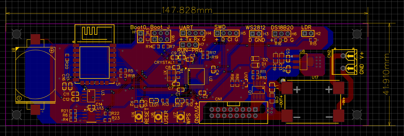
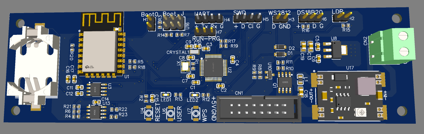
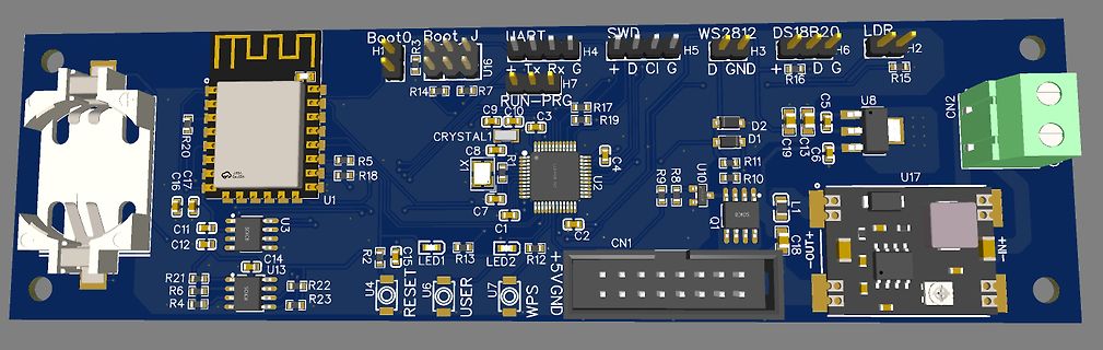
PCB-Layout einer Mikrocontroller-Platine
147.828mm 41.910mm Boot0 Boot J UART H4 H5 H3 H6 H2 SWD D C I G D GND D G LDR WS2812 DS18B20 R14 R7 R15 R20 C7 C16 R5 R18 U1 CRYSTAL C8 C9 C3 R17 R19 C11 C12 C14 U3 R21 R6 R4 R22 R23 U13 LED1 R13 LED2 R2 R12 C1 C2 C18 U4 RESET U6 USER U7 WPS 5V GND CN1 CN2 U2 U17 GND V+
in „WordClock mit WS2812“ · Projekte & Code · · Layouts
-
PDF
AMIS-30543-D.pdf
important circuit that guarantees circuit. Each driver transistor has an individual detection bit low R DS(on) for all drivers, especially for low supply (see Table 14 SPI Status Registers Address SR1 and SR2: voltages. If supply voltage is too low or external components <OVCXij> and <OVCYij>). Error condition is latched are not properly connected to guarantee R DS(on) of the and the microcontroller needs to clean the status bits to drivers, then the bit <CPFAIL> is set (Table 14). Also after reactivate the drivers. POR the charge pump voltage will need some time
in „Puls aus Sinuswelle herausrechnen“ · Mikrocontroller und Digitale Elektronik ·
-
PDF
DP-5_Electronic.pdf
P00 D 0 Q0 a ZC2 7 8 ZC 3 U 4 C4 S W1 4 1A2 1Y 2 16 P01 4 D 1 Q1 5 b a 9 10 b U 5 C2 S W2 6 1A3 1Y 3 14 P02 7 D 2 Q2 6 c c 11 12 d U 6 C1 S W3 8 1A4 1Y 4 12 P03 8 D 3 Q3 9 d e 13 14 f U 7 C5 S W4 11 2A1 2Y 1 9 P04 13 D 4 Q4 12 e g 15 16 dp U 8 C8 S W5 13 2A2 2Y 2 7 P05 14 D 5 Q5 15 f S0 17 18 S1 U 9 C9
in „Winbond w78e52-24 mit Nuvoton w78e052DDG ersetzen“ · Mikrocontroller und Digitale Elektronik ·
-
Datei
main.cpp
30), t2min(8, 00), t2min(8, 00)}; // time in minutes i.e. h*60+min uint16_t stop_time[7] = {t2min(14, 00), t2min(14, 00), t2min(14, 00), t2min(14, 00), t2min(14, 00), t2min(12, 00), t2min(12, 00)}; uint8_t status[7] = {AKTIV, AKTIV, AKTIV, AKTIV, AKTIV, INAKTIV, INAKTIV}; // aktiv/inaktiv String config_file
in „Absturz beim ESP8266“ · Mikrocontroller und Digitale Elektronik ·
-
PDF
SED1565.pdf
NC) –1086 101 COM15 1163 22 D5 2461 62 V 3 –1176 102 COM15 1090 23 D6, SCL 2342 63 V 3 –1265 103 COM14 1017 24 D7, SI 2222 64 V 4 –1354 104 COM14 945 25 (NC) 2119 65 V 4 –1443 105 COM13 872 26 VDD 2030 66 V 5 –1532 106 COM13 799 27 VDD 1941 67 V 5 –1621 107 COM12 727 28 VDD 1852 68 (NC) –1710 108 COM12
in „Pollin 128x64 GLCD : Bild verzerrt“ · Mikrocontroller und Digitale Elektronik ·
-
 Bild
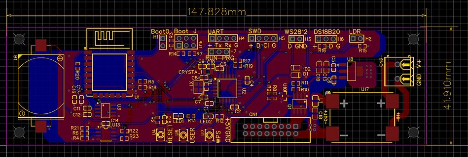
CAD-Ansicht eines Leiterplatten-Layouts
Boot0, Boot J, HART, SWD, WS2812, DS18B20, LDP, H1, H4, H5, H3, H2, U16, R14, R7, R17, R19, R15, R16, D, C, I, G, GND, U8, C5, C15, C19, D2, D1, C16, R20, C7, C9, C10, C3, C8, LX, U2, C4, U1, R5, R18, R8, R9, U10, R11, R10, C6, C1, C2, CN1, U3, C11, C12, R2, C14, U17, L1, C18, OUT, +IN, R21, R4, U13, R22, R23, U4, RESET, U6, USER, LED1, LED2, R13, R12, WPS, +5V, GND
in „WordClock mit WS2812“ · Projekte & Code · · Layouts
-
Datei
sub_irMenu.c
=kkdat[5]*10+kkdat[6]; MON=kkdat[7]*10+kkdat[8]; YEA=kkdat[9]*10+kkdat[10]; //wdg20on; #if use_twi ds1307gefunden = i2c_start(0xd0); //0b11010000 - 188?? if (ds1307gefunden==0){ kk_ds1307_setAll();lcd_write(" ok....");}else{lcd_write("err1307");} #endif ir_cmd=10; //wdg20off; //no break case(10):ir_cmd
in „RC5 code einer IR Fernbedienung auslesen“ · Mikrocontroller und Digitale Elektronik ·
-
Datei
TS_iP158_C0802_4BIT_44780_P1f-2.h
für 4Bit-daten genutzt // | | // | P3.0| CS1 SPI frei (28) // UTXD0 |P3.4 P3.1|-> Daten Ausgang I2C DS32C35 (29) // URXD0 |P3.5 P3.2|<- Data In (SOMI0) I2C DS32C35 (30) // UTXD1 |P3.6 P3.3|-> (UCLK) I2C DS32C35 (31) // URXD1 |P3.7 // // | P4.0-P4.7| (36)..(43) //(44)SD-CS |P5.0 P2.7| SD Karte Einsteckkontrolle
in „LCD im 4-Bit Modus an nur einem Port betreiben“ · Mikrocontroller und Digitale Elektronik ·
-
PDF
BERECHNUNG_TEMPERATUR.pdf
DS18s22 reale 9-BIT COUNT 9-BIT aufbereitet Tempweratur (SCRATCHPAD) REMAIN (BIT0-ausgeblendet) (SCRATCHPAD) 1,1875 1,0 9 1 1,1875 1,1250 1,0 10 1 1,1250 1,0625 1,0 11 1 1,0625 1,0000 1,0 12 1 1,0000 0,9375 1,0 13 1 0,9375 0,8750 1,0 14 1 0,8750 0,8125 1,0 15 1 0,8125 0,7500 1,0 16 1 0,7500 0,6875 0,5 1 0 0,6875 0,6250 0,5 2 0 0,6250 Berechnung nach Formel 0,5625 0,5 3 0 0,5625 0,5000 0,5 4 0 0,5000 0,4375 0,5 5 0 0,4375 0,3750 0,5
in „DS1820 DS18s20 Digital Thermometer 1-wire Beispiele ATmega8 Assembler“ · Projekte & Code ·
-
Datei
nRF24L01.h
TX_ADDR 0x10 #define RX_PW_P0 0x11 #define RX_PW_P1 0x12 #define RX_PW_P2 0x13 #define RX_PW_P3 0x14 #define RX_PW_P4 0x15 #define RX_PW_P5 0x16 #define FIFO_STATUS 0x17 /* Bit Mnemonics */ #define MASK_RX_DR 6 #define MASK_TX_DS 5 #define MASK_MAX_RT 4 #define EN_CRC 3 #define CRCO 2 #define PWR_UP
in „Problem Linken von nRF24 Multi Network mit AVR Studio“ · Mikrocontroller und Digitale Elektronik ·
-
Datei
nRF24L01.h
TX_ADDR 0x10 #define RX_PW_P0 0x11 #define RX_PW_P1 0x12 #define RX_PW_P2 0x13 #define RX_PW_P3 0x14 #define RX_PW_P4 0x15 #define RX_PW_P5 0x16 #define FIFO_STATUS 0x17 #define DYNPD 0x1C /* Bit Mnemonics */ /* configuratio nregister */ #define MASK_RX_DR 6 #define MASK_TX_DS 5 #define MASK_MAX_RT
in „NRF24L01+ mit ATMEGA328P Standalone“ · Mikrocontroller und Digitale Elektronik ·
-
Datei
nRF24L01.h
TX_ADDR 0x10 #define RX_PW_P0 0x11 #define RX_PW_P1 0x12 #define RX_PW_P2 0x13 #define RX_PW_P3 0x14 #define RX_PW_P4 0x15 #define RX_PW_P5 0x16 #define FIFO_STATUS 0x17 #define DYNPD 0x1C /* Bit Mnemonics */ /* configuration register */ #define MASK_RX_DR 6 #define MASK_TX_DS 5 #define MASK_MAX_RT
in „nrf24l01 sendet nicht“ · Mikrocontroller und Digitale Elektronik ·
-
Datei
nRF24L01.h
TX_ADDR 0x10 #define RX_PW_P0 0x11 #define RX_PW_P1 0x12 #define RX_PW_P2 0x13 #define RX_PW_P3 0x14 #define RX_PW_P4 0x15 #define RX_PW_P5 0x16 #define FIFO_STATUS 0x17 #define DYNPD 0x1C /* Bit Mnemonics */ /* configuratio nregister */ #define MASK_RX_DR 6 #define MASK_TX_DS 5 #define MASK_MAX_RT
in „NRF24L01 und Atmega328P“ · Mikrocontroller und Digitale Elektronik ·
-
PDF
imt902_datenblatt.pdf
85.4 kHz. chop CR -7- IC Power Dissipation: Power consumed by the Power Transistor (calculated with DS ON= 0.6 Ω): 2 P(out)=2( )* out )* DS( )= 2* out*RDSon Power consumed by the logic block: Operating mode / unit whenDDis connected to 5V anM V is connected to 24V: P= 5( )*0.002( )+ 24( )*0.0125( ) =
in „Urgestein IMT902 Motortreiber Schaltplan - Kritik erwünscht!“ · Mikrocontroller und Digitale Elektronik ·
-
PDF
Raspberry_BCtrl.pdf
+3,3 V k 2 2 R 4 1 3 JP1 S S 1 2 1 1 VDD DQ 3 4 5 6 DS18S20 7 8 IC2 IC 9 10 6 11 12 13 14 R6 15 16 17 18 1k 19 20 R7 21 22 23 24 1k 25 26 0 R2 8 0 1 0 R 1 R 1 270 LED1 R3 270 LED2 R4 bestellt bei hbe-shop.de 270 LED3 E E E E IC1 R5 4 S3 S2 S S 1 16 1 1 1 1 2 15 270 R A R A R A R A 3 14 LED4 4 13 5 12 6 11 7 10 8 9 MCP3008 26.02.2013 12:55:39 D:\privat\Raspberry_BCtrl.sch (Sheet: 1/1)
in „Raspberry Pi - Evalboard v1“ · Mikrocontroller und Digitale Elektronik ·
-
PDF
CamperDisplay.pdf
C25 C26 C27 DGND 3 0 C DGND C3 C4 C11 , 110A 3 + FILL25 5 + + 0 4 +3,3V C20 0 V 2 1 R C21 EXTRESET U14 4 6 8 9 1 GND P5 X - OUT25 OUTWASTE 1 CLK SCL 8 SCL 2 3 4 2 1 0 WATERREF 0R0 4 - V 2 VCC DS3231 SDA 7 D D D A MOS2 IN BTS410 2 N R20 100nF 2 LM339 C15 3 6 SDA 10nF 7 p D 7 V V V D K 8 3 VDD N 1 INT VBAT
in „Akku und Wasserstandsdisplay für Wohnmobile“ · Projekte & Code ·
-
PDF
VHF-COMM.1984.2--b.pdf
spread wnh narrow-band Interference. 119 VHF-COMMUNICATIONS 2/84 Cnrrolalor Fig.4: "~, Behaviour 01a DS system in th e Case of interlerence; narrow ~ ~ I - band interference (ew), DS Sg l31 1"I",on,""rno<I wideband inte rlerence Ca"'", (e.gDS) ~ _ 0 _ (;Wi"t~,!"'e"r", os :=;")" '1 "ar,"~ Spre~dl~oI"r""
-
PDF
VHF-COMM.1984.2.pdf
spread wnh narrow-band Interference. 119 VHF-COMMUNICATIONS 2/84 Cnrrolalor Fig.4: "~, Behaviour 01a DS system in th e Case of interlerence; narrow ~ ~ I - band interference (ew), DS Sg l31 1"I",on,""rno<I wideband inte rlerence Ca"'", (e.gDS) ~ _ 0 _ (;Wi"t~,!"'e"r", os :=;")" '1 "ar,"~ Spre~dl~oI"r""
-
PDF
HF_Attenuator_Package_v1.pdf
+5V(JP2) HF S-Parameter Test Set: Attenuator C107 0.1u FB100 C104 0.1u 14 C108 U100 C102 1u 100p C100 2 9 2 9 2 9 R105 1,3,5 R103 1n P100 J120 1k 2,4,6 24.9 1 3 8 3 8 3 8 C105 X RL100 RL110 RL120 X R107 100p 74HC14 RL100 ROutDS 5,6 5,6 5,6 Transfer P130 100k Switch R104 X
in „Bistabiles Relais ansteuern“ · Mikrocontroller und Digitale Elektronik ·
-
PDF
HF_Attenuator_Package_v1.pdf
+5V(JP2) HF S-Parameter Test Set: Attenuator C107 0.1u FB100 C104 0.1u 14 C108 U100 C102 1u 100p C100 2 9 2 9 2 9 R105 1,3,5 R103 1n P100 J120 1k 2,4,6 24.9 1 3 8 3 8 3 8 C105 X RL100 RL110 RL120 X R107 100p 74HC14 RL100 ROutDS 5,6 5,6 5,6 Transfer P130 100k Switch R104 X
in „bistabiles Relais für AVR/Arduino“ · Mikrocontroller und Digitale Elektronik ·
-
PDF
Soldering_Iron_schematics.pdf
OLED-Display Thermocouple ADC GPIO-Expander 3V3 1 2 R R ▯A 3V3 3V3 3V3 ▯A U7 ▯ ▯ R13 10k▯' 1A0 VCC 16 0 0 U8 R14 10k▯' 2A1 SDA 15 IO4/SDA 1 1DS1021-2x7SF11-B 1 1 GND N.C. 8 R15 10k▯' 3A2 SCL 14 IO5/SCL U9 R 2 T- SO 7 IO12/SO P0/SW 4P0 INT# 13 R17 P0/A 1 2 T+ 3 T+ CS# 6 IO15/CS P1/CLK 5P1 P7 12 10k▯' C23 3 1 2 4
in „ESP gesteuerter JBC T245 Lötkolben mit USB-C PD - Schematic review“ · Mikrocontroller und Digitale Elektronik ·
-
 Bild
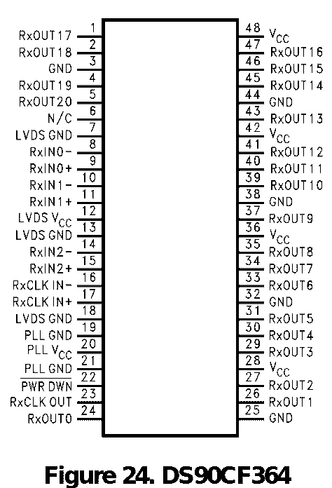
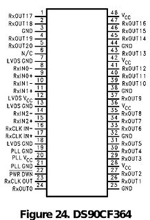
Pinbelegung des DS90CF364 ICs
4 RxOUT19 5 RxOUT20 6 N/C 7 LVDS GND 8 RxIN0- 9 RxIN0+ 10 RxIN1- 11 RxIN1+ 12 LVDS Vcc 13 LVDS GND 14 RxIN2- 15 RxIN2+ 16 RxCLK IN- 17 RxCLK IN+ 18 LVDS GND 19 PLL GND 20 PLL Vcc 21 PLL GND 22 PWR DWN 23 RxCLK OUT 24 RxOUT0 25 GND 26 RxOUT1 27 RxOUT2 28 Vcc 29 RxOUT3 30 RxOUT4 31 RxOUT5 32 GND 33 RxOUT6
in „10,4" Display Ersatz für Messgerät gesucht“ · Analoge Elektronik und Schaltungstechnik · · Screenshots
-
PDF
TDA8703_PHI.pdf
supply current − 28 36 mA CCD digital supply current − 19 25 mA CCO output stages supply current − 11 14 mA ILE DC integral linearity error − − ±1 LSB DLE DC differential linearity error − − ±1/2 LSB AILE AC integral linearity error note 1 − − ±2 LSB B −3 dB bandwidth note 2;CLK = 40 MHz − 19.5 − MHz CLK
in „TDA 8703 AD Wandler“ · Mikrocontroller und Digitale Elektronik ·
-
PDF
TDA8703_3.pdf
supply current − 28 36 mA CCD digital supply current − 19 25 mA CCO output stages supply current − 11 14 mA ILE DC integral linearity error − − ±1 LSB DLE DC differential linearity error − − ±1/2 LSB AILE AC integral linearity error note 1 − − ±2 LSB B −3 dB bandwidth note 2;CLK = 40 MHz − 19.5 − MHz CLK
in „TDA 8703 AD Wandler, Entkopllungsfragen“ · Mikrocontroller und Digitale Elektronik ·
-
PDF
heds-1300.pdf
12.0 R.P. MAXIMUM SIGNAL POINT – MSP (0.473) (0.200) REFERENCE PLANE CL 8.33 (0.328) 7.79 (0.307) 1.14 (0.045) 0.73 (0.029) 5.08 4.27 ± 0.25 Z 15.24 (0.600) (0.200) (0.168 ± 0.010) 0.73 (0.029) 12.70 (0.500) 11.50 (0.453) 11.22 (0.442) 1. ALL DIMENSIONS IN MILLIMETERS AND (INCHES). 2. ALL UNTOLERANCED
in „Kugelschreiber mit Barcodescanner bei Pollin“ · Mikrocontroller und Digitale Elektronik ·
-
Datei
gP000-FKA44780.h
| P2.0|Taster für Programmwahl //8 MHz X2OUT- | P1.0..P1.7|Daten FKA // | | // | P3.0|Gate MOSFET DS2482-DS18B20 // a.B. UTXD0 |P3.4 P3.1|<-> SDA Daten Leitung I2C (29) a.B.= nicht angeschlossen // a.B. URXD0 |P3.5 P3.2| (30) // i.B. UTXD1 |P3.6 P3.3| -> SCL Serial Clock Out (UCLK) (31) i.B. in Betrieb
in „LCD-Modul TC1602E-01 von Pollin ansteuern“ · Mikrocontroller und Digitale Elektronik ·
-
PDF
datenblatt-1183521-infineon-technologies-btm7810k-pmic-voll-halbbrueckentreiber-induktiv-dmos-pg-to263-15.pdf
Free configurable as bridge or quad-switch • Optimized for DC motor management applications • Low R DS ON High side: 26 mΩ typ. @ 25°C, 65 mΩ max. @ 110°C Low side: 14mΩ typ. @ 25°C, 28 mΩ max. @ 110°C • Maximum peak current: typ. 42 A @ 25 °C • Very low quiescent current: typ. 4 μA @ 25 °C PG-TO263-15
in „MosFET über PWM ansteuerbar?“ · Analoge Elektronik und Schaltungstechnik ·
-
PDF
slau157o_CCS.pdf
Using Code Composer Studio (CCS) ....................................................................14............. 2.1.1 Creating a Project From Scratch .................................................................14............ 2.1.2 Project Settings .............................................
in „MSP430 - erstes Debuggen - valid setup“ · Mikrocontroller und Digitale Elektronik ·
-
Datei
fft232.asm
nop ;Sync verlängern nop nop sbi portd, Sync ; component, 2nd value is fundamental freq sendl: rcall ds_hl ; and last value is highest freq) subi DL, 8 brcc sendl ret ds_hl: ldiw Y, LvlBuf+1 ldi CL, FFT_N/4 ;CL=64 senl: ld AL, Y+ ;1-12 cpi CL, 4 ;54-63 brlo make4p cpi CL, 8 ;41-53 brlo make3p cpi CL, 20
in „Schnelle FFT in Assembler“ · Digitale Signalverarbeitung / DSP / Machine Learning ·
-
Datei
rfm70.cpp
0x00, 0x00}, {0x00, 0x12, 0x73, 0x00},//12 {0x36, 0xB4, 0x80, 0x00}, }; static PROGMEM uint8_t set1_14[]={0x41,0x20,0x08,0x04,0x81,0x20,0xCF,0xF7,0xFE,0xFF,0xFF}; static PROGMEM uint8_t set0[][2]={ {0,0x3F}, //mask RX_DR\TX_DS\MAX_RT (we do not use IRQ!),Enable CRC ,2byte,POWER UP,PRX {1,0x01}, //Enable
in „Arduino RFM70“ · Mikrocontroller und Digitale Elektronik ·
-
PDF
Support-Schematic.PDF
SIPO-SRCK PCpt11 11 12 PCpt112 SIPO-RCK PCbe01 11 12 PCbe0PISO-PL R66 P I 3 C 11B 2 4B PI121013 PIP16O101DS P0 PI6ISO107 PIP4011 2 PIP402 SIPO-RCK PCpt11313 14 PCpt11PISO-OUT GND BLINK PCbe03 13 14 PCbe0CHESS-RESERVEDE 10K P I 4 C 11Y 3 4A PI111012 31 PISO-CPCP 3.3V PIP10O101VDD P1 PI5ISO106 PIP4033 4 PIP404
in „Projekt: Schachcomputer mit OLED-Display, Gehäuse aus Holz (open source)“ · Mikrocontroller und Digitale Elektronik ·
-
PDF
2009101102_Senba-Sensing-Tech-BS612_C389589.pdf
/64VDD 1M 487K 12 300 11/32VDD~12/32VDD 23/64VDD 1M 560K 13 600 12/32VDD~13/32VDD 25/64VDD 1M 634K 14 900 13/32VDD~14/32VDD 27/64VDD 1M 732K 15 1800 14/32VDD~16/32VDD 29/64VDD 1M 825K 16 3600 15/32VDD~16/32VDD 31/64VDD 1M 953K V 1.0 5 www.nysenba.com 5. 灵敏度设置 SENS输入的电压设定了灵敏度阀值,这个阀值用于检测PIRIN和NPIRIN输入的
in „PIR-Sensor wird von BME680 gestört, warum?“ · Mikrocontroller und Digitale Elektronik ·
-
PDF
S-80825CNNB-B8K-T2.pdf
0.093 0.110 Current consumption I V =1.5 V S-80808 to 09 1.3 3.5 µA 2 SS DD VDD2.0 V S-80810 to 14 1.3 3.5 Operating voltage V DD 0.65 5.0 V 1 Output current IOUT Output transistor, 0.04 0.2 mA 3 Nch, VDS0.5 V, VDD0.7 V Output transistor, Pch, V =2.1 V, V =4.5 V 2.9 5.8 4 DS DD Response
in „Unbekanntes SMD Bauteil auf einer Fahrradrücklicht-Platine“ · Analoge Elektronik und Schaltungstechnik ·
-
PDF
AP9101C.pdf
Operating Conditions Symbol Parameter Min Max Unit V Supply Voltage (Between VDD and VSS) 1.5 5.5 V DS V DM Charger Input Voltage (Between VDD and VM) -0.3 5.5 V TA Operating Ambient Temperature -40 +85 °C AP9101C 4 of 26 November 2018 Document number: DS37771 Rev. 7 - 2 www.diodes.com © Diodes Incorporated
in „LiPo Tiefentladeschutz 1S/Einzel-Zellen "Mini/Nano"“ · Platinen ·
-
PDF
pcm1716.pdf
4 6 8 10 12 14 16 18 20 0 2 4 6 8 10 12 14 16 18 20 Frequency (kHz) Frequency (kHz) DE-EMPHASIS FREQUENCY RESPONSE (f = 48kHz) DE-EMPHASIS ERR0R (f = 48kHz) 0 S S 0.5 B –2 B 0.3 ( –4 ( 0.1 e e e –6 e–0.1 L –8 L–0.3
in „DAC über SPI configurieren??, Codevision“ · Mikrocontroller und Digitale Elektronik ·
-
PDF
Induktive_Pfeilgeschnwindigkeitsmessung.pdf
density and C(s) is the area of the cross-section. The mass of one limb is then given by Z L 1 m b ρC(s)ds = ρC(2)L . (2) 0 The relationship between the loading and the deformation is derived by use of the Euler-Bernoulli equation: 2 d x M ds2 = EI (3) where M is the bending moment at s. When the limb is
in „Geschwindigkeitsmesser für Pfeile psf“ · Mikrocontroller und Digitale Elektronik ·
-
PDF
Induktive_Pfeilgeschnwindigkeitsmessung.pdf
density and C(s) is the area of the cross-section. The mass of one limb is then given by Z L 1 m b ρC(s)ds = ρC(2)L . (2) 0 The relationship between the loading and the deformation is derived by use of the Euler-Bernoulli equation: 2 d x M ds2 = EI (3) where M is the bending moment at s. When the limb is
in „Welcher µC passt? Pfeilgeschwindigkeit messen“ · Mikrocontroller und Digitale Elektronik ·
-
PDF
R__ckmelder.pdf
Q2 10 E 2 A 2 GND S2 11 S2 P/S P/S S2 R0 3 3 S1 S3 CLK CLK 100NF1 2 P2 C3 S3 R0 Reset 4 Reset 4 GND 14 R3 P4 Q3 1 IC1 5 5 +5V 100NF S2 S3 15 S3 GND GND 2ND 2N2 2 2 2 GND C4 1 2 P3 6 5 6 7X 0 0 6 GND +5V +5V 1+5V 1+1V 1 1 1 Data_Out K K KK K K S3 +5V 11 DS 100NF1 2 5 STROBE P4 P1 7 P1 Data +5V +5V P2 6
in „Störungen bei Rückmelder“ · Mikrocontroller und Digitale Elektronik ·
-
PDF
CD4066BC.pdf
, and analog-signal-gain Ordering Code: Order Number Package Number Package Description CD4066BCM M14A 14-Lead Small Outline Integrated Circuit (SOIC), JEDEC MS-012, 0.150" Narrow CD4066BCSJ M14D Pb-Free 14-Lead Small Outline Package (SOP), EIAJ TYPE II, 5.3mm Wide CD4066BCN N14A 14-Lead Plastic Dual-In-Line
in „Schaltung so richtig?“ · Mikrocontroller und Digitale Elektronik ·
-
PDF
C17410452.pdf
Operational Description ------------------------------------------------------------------------------- 14 10.1 Startup Operation--------------------------------------------------------------------------------- 14 10.2 Undervoltage Lockout (UVLO) ---------------------------------------------------------------- 14 10.3 Bias Assist Function------------------------------------------------------------------------------- 14 10.4 Soft Start Function-------------------------------------------------------------------
in „Test in der Schaltung STR3A400“ · Analoge Elektronik und Schaltungstechnik ·
-
PDF
sepic-wanlder.pdf
governing the selection of the MOSFET are the minimum threshold voltage V , the on-resistance R th(min) DS The inductor value is calculated by: (ON),gate-drainchargeQ GD,andthemaximumdraintosource voltage, V DS(max). Logic level or sublogic-level threshold MOSFETs should be used based on the gate drive voltage
in „Sepic-Wandler“ · Analoge Elektronik und Schaltungstechnik ·
-
PDF
Schaltplan.pdf
SV1 DS3231 40 39 38 37 R3 1 32KHZ SCL 16 36 35 4,7K R4 34 33 2 VCC SDA 15 32 31 30 29 3 14 4,7K 28 27 INT VBAT 26 25 4 13 24 23 RST GND G1 22 21 5 P$1 P$8 12 - + 20 19 18 17 6 11 CR2032H 16 15 P$2 P$7 14 13
in „(Suche Dienstleistung) Ne555 schaltung erstellen“ · Markt ·
-
PDF
Display.pdf
output pin : 64 x 128 pins ¥ Segment display output pin : 3 x 12 pins LCD drive system : +4.0 to +14.0 V ¥ Icon display output pin : 1 x 1 pin ¥ Operating temperature : —30 to +85 ßC ¥ Package : 260-pin TCP (Tape Carrier Package) ¥ LCD display by graphic display RAM — Normal mode : RAM data "0"/not
in „LC-Display Sharp M078CKA ansteuern“ · Mikrocontroller und Digitale Elektronik ·
-
PDF
lh155.pdf
output pin : 64 x 128 pins ¥ Segment display output pin : 3 x 12 pins LCD drive system : +4.0 to +14.0 V ¥ Icon display output pin : 1 x 1 pin ¥ Operating temperature : —30 to +85 ßC ¥ Package : 260-pin TCP (Tape Carrier Package) ¥ LCD display by graphic display RAM — Normal mode : RAM data "0"/not
in „Suche sehr dünnes Grafikdisplay“ · Mikrocontroller und Digitale Elektronik ·
-
PDF
lh155.pdf
output pin : 64 x 128 pins ¥ Segment display output pin : 3 x 12 pins LCD drive system : +4.0 to +14.0 V ¥ Icon display output pin : 1 x 1 pin ¥ Operating temperature : —30 to +85 ßC ¥ Package : 260-pin TCP (Tape Carrier Package) ¥ LCD display by graphic display RAM — Normal mode : RAM data "0"/not
-
PDF
ZN425E.pdf
THIS DOCUMENT IS FOR MAINTENANCE PURPOSES ONLY AND IS NOT RECOMMENDED FOR NEW DESIGNS MAY 1994 DS3005-2.0 ZN425E8 8-BIT D-A/A-D CONVERTER The ZN425 is a monolithic 8-bit D-A converter containing an R-2R ladder network of diffused resistors with precision bipolar switches, and in addition a counter
in „Digital Analog Converter“ · Mikrocontroller und Digitale Elektronik ·