Corporation 273 FLASHlogic Programmable Logic Device Family Data Sheet SRAM Configuration Each FLASHlogic LAB can be configured as a 128 10 (128 words by 10 bits) SRAM block, as shown in Figure 6. The SRAM block can be definedwitheitherabidirectional I/Odatabusorwithseparateinputand output data buses. Figure 6.
the clock can be stopped – Power-down mode without loss of user data and then the execution resumed from the CMOS and TTL compatible point the clock was stopped. TWO speed ranges at V CC = 5V SELECTION TABLE – 0
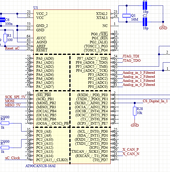
Bäumen nicht mehr. Ich möchte eine simple SPI Kommunikation zum laufen bringen. Hierbei wird der AT90CAN128 als Master initialisiert und der ATmega16 als Slave. Es soll der Master den Slave ansprechen über den SS Pin (low) und der Atmega soll in diesem Projekt dann mit den ausgewerteten Sensordaten
Max schrieb im Beitrag #7750080: > AT90CAN128.PNG > ATmega16.PNG An _jedem_ VCC Pin _ein_ Abblock-Kondensator gegen Masse. An _jedem_ ! Max schrieb im Beitrag #7750080: > aus dem Schaltplan mit rangehangen. Nein! .... aus
more space on the screen is desired, this option can be chosen to hide the toolbar. Selecting it a second time will show the toolbar again. It may be useful to note that the toolbar can be undocked from the main screen and made to “float” at a user-defined
Anwendung auf einen Mega2560. Das Problem kommt, wenn der µC noch mehr zu tun hat. Ein Arduino mit AT328 und kleinem OLED 128x64 funktioniert. SD-Karte ist auch kein Problem, ebenso das Messen von Spannungen. Ich bin dann aufs Maul gefallen, weil seine Ressourcen nicht genügen, alles gemeinsam auszuführen
JTdCJTIyY2F0ZWdvcnlkcm9wZG93biUyMiUzQSU1QiUyMk1pY3JvY29udHJvbGxlcnMlMjBhbmQlMjBNaWNyb3Byb2Nlc3NvcnMlMjIlMkMlMjIlMjIlMkMlMjIlMjIlNUQlN0Q= Schade, nur die beiden bisherigen Typen mit nur einem CAN (AT90CAN*, ATmega*M1).
operation starts lock Bypass Program command can be used to the Program/Erase Controller about 50µs after the program one address in memory at a time. The last Bus Write operation. Once the Program/Erase command requires two Bus Write operations,
DC Motors Characteristics: ultra long life with 2 ball bearings, used for a secondary air pump, it can operate at high tem Specifications: Dimensions : Ø 52.0 X 85.0 mm Shaft Diameter : Ø 6.005 mm Input Voltage : 13.0 V DC No Load Speed : 6400 rpm Stall Torque : 915.92 mNm Maximum Output Power : 153.63
kommuniziert: [c] 6½ digit resolution • ±0.2 V, ±2 V, and ±20 V range • Dual channel • 90 days accuracy: <17 ppm of reading range at 2 V range • <0.225 ppm RMS noise of 2 V range at 1 NPLC, 1000 samples • Up to 1 kSPS data rate [/c] 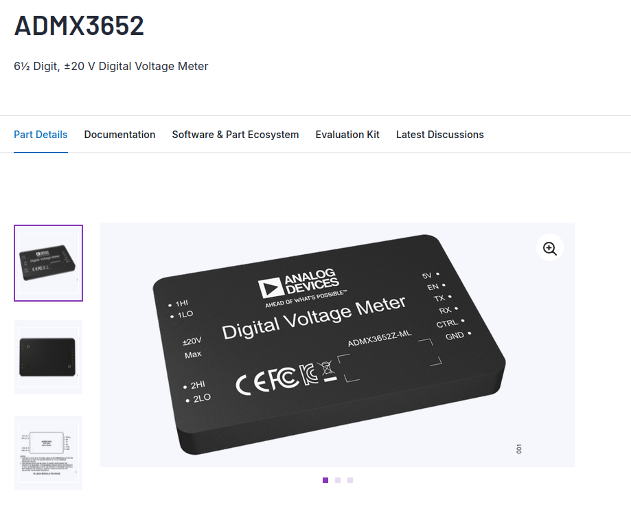 Bildquelle
sensor, ZMOD4410 gas sensor, and the HS4003 humidity and temperature sensor. Together, these sensors can detect particulate matter, total volatile organic compounds (TVOC), estimated CO2, temperature, and humidity all in one system. All key components have been pre-integrated and fully calibrated at the
provided if necessary. The currently valid version 2021_10 is available for download as a PDF file at http://www.dimplex.de/downloads . You can find this under the manual category, via the search function or via the following link. It cannot be concluded from the publication that the solutions described
.) can be calculated by using the potentials at the postprocessing stage. Capacitance, inductance, energy, force and other quantities can also be calculated. The postprocessing give a chance to modify the
? A. The AT17C/LVxxx devices are pin and functionally compatible with all available 17xxx parts from Xilinx, Altera (EPCxxx) and AT&T. Q. Can I use the Atmel parts to program my Xilinx FPGAs ? A. Atmel devices
operation to store variables and data or stacks during program execution. The maximum capacity is 128KB. SRAM supports read-write access of byte, half-word and word. SRAM supports code running (supports access of SBus, ICode and DCode), and can run programs at full speed in SRAM. The maximum address
determines level (optocoupler LED voltage drop plus Zener voltage), the the appropriate current limit. At high loads, when the EN/UV optocoupler LED will start to conduct, pulling the EN/UV pin pin is high (less than 2µAout of the pin), a switching cycle low. The Zener diode can be replaced by a TL431 reference
harmonic distortion At any level up to rated power, into 4 or 8 ohms <0.05% (20Hz – 20kHz) Typically <0.005% at 1kHz Frequency response +-0.2dB (20Hz – 20 kHz) -1dB at 1Hz and 100kHz Residual hum and noise Referenced to full
BD35F-HD and BD1.4F-VSD-HD are new versions the need for current batteries if an ice bank is used which can handle extreme vibrations. for energy storage.When storing the sun energy in ice packs the cabinet can be kept at desired BD35F-B (Bus-optimized) temperatures both night and day. The BD35F-B is a special
2 G Sattler, DJ4LB 1973/2 66 - 80 Television 2 m Band A 144 MHz Linear Amplifier with 25 W Output at 12 V to 14 V G Otto, DC6HL 1973/2 81 - 90 Measuring A Dual Input Preamplifier with 2:1 Prescaler for Frequency Counters from W R Kritter, DL8TM 1973/2 91 - 94 Technology 1 Hz to Min 100 MHz Measuring
is write cycle. shifted out on the SO pin. Data stored in the memory at 6.1 SRAM/RTCC Registers the next address can be read sequentially by continuing to provide clock pulses to the client. The The RTCC registers are located at addresses 0x00 to internal Address Pointer
type used in this mainboard is 8Kx8, 16Kx8, 32Kx8 and the DATA SRAM type is 32Kx8-15ns 64Kx8-15ns or 128Kx8-15ns. The mainboard can be installed with 128, 256, 512 KB cache memory when using 32Kx8 or 64Kx8 or 128Kx8 type DATA SRAM respectively. • CACHE MEMORY SIZE SETTING 3-3 GA-5486AL Size 128K 256K 512K JP4 2-4 OPN SHT SHT JP4 1-3 OPN OPN SHT DATA SRAM 32K8 4 pcs 64K8 4 pcs 128K8 4 pcs TAG SRAM 8K8 16K8 32K8 JP4 JP4 JP4 4 2 4 2 4 2 3 1 3 1 3 1 128KB 256KB 512KB 3.5 CPU INSTALLATION AND JUMPERS SETUP The CPU is a sensitive electric component and it can be easily damaged by
Apps Can Quickly Destroy Your Mobile’s Flash: Why They Don’t, and How to Keep It That Way Tao Zhang Aviad Zuck The University of North Carolina at Chapel Hill Technion – Israel Institute of Technology zhtao@
register P1SCLMD, the PHY special control/status and LinkMD register (0xF4). 3.2.9.2 Usage LinkMD can be run at any time by ensuring that Auto-MDIX has been disabled. To disable Auto-MDIX, write a ‘1’ to P1CR[10] to enable manual control over the pair used to transmit the LinkMD pulse. The self-clearing
If you are interested in participating in the activities of the SFF TWG, the membership application can be found at: http://www.snia.org/sff/join The complete list of SFF Specifications which have been completed or are currently being worked on can be found at: http://www.snia.org/sff/specifications/SFF
of our feeders. As Component dip time 0 - 2 s a result of this, it can be installed (dwell time in material film) (in 0.1 s increments) at any location in the feeding area. Number of programmable acceleration 100 The flux, respectively the isotropi- values for the upward
The W25Q64FV array is organized into 32,768 programmable pages of 256-bytes each. Up to 256 bytes can be programmed at a time. Pages can be erased in groups of 16 (4KB sector erase), groups of 128 (32KB block erase), groups of 256 (64KB block erase) or the entire chip (chip erase). The W25Q64FV has
can be driven or read through software control, independent of serial port activity. CP3/CTS/DCD 8 CP3 can be configured as follows: (Configurable Pin 3) • Flow control: CTS (Clear to Send) input read by
befüllt. Wir haben aber noch zusätzlich einen Message-FIFO im SRAM angelegt. Später haben wir den AT89C51CC03 und den AT90CAN128 verwendet. Der CAN-Controller ist bei allen 3 gleich aufgebaut, d.h. auch 15 MOBs. Zur Programmierung gibt es nicht viel zu sagen. Man setzt die Timingregister für die
Off Isolation RL= 50 Ω at 2.7 GHz (See Figure 18) –28 dB RL= 50 Ω at 4.05 GHz (See Figure 18) –25 Port A at DC –0.75 IL Insertion Loss dB Port B at DC –1 Differential Bandwidth Port A RL= 50 Ω, All channels (See Figure 19) 6.9
n from 1 to 4095 are valid. When the Timer Value is set to 0, the countdown timer does not start. At the end of every countdown, the timer sets the Periodic Countdown Timer Flag (bit TF in Status Register). The TF flag can only be cleared by command. When enabled, a pulse is generated at the interrupt
Guten Abend, dies ist ein Nachfolgethread von CAN-Bibliothek für den at90CAN128 und das AVRStudio vom 29.04.2008. Verwendet hab ich den Programmcode von Daniel S. vom 15.02.2013. Der Compiler läuft ohne Fehler durch. Nur leider bekomme ich keine CAN Botschaft in CANoe angezeigt. Ich verwende: µC: AT90CAN128 Transceiver: TJA1050 Entwickerumgebung: Atmel Studio 7 Kann mir bitte jemand helfen, warum ich keine Botschaft in CANoe empfange.
illustrates, changing the TOP actively while the Timer/Counter is running in the phase correct mode can result in an unsymmetrical output. The reason for this can be found in the time of update of the OCRnx Register. Since the OCRnx update occurs at TOP, the PWM period starts and ends at TOP. This implies
electrical/mechanical failure modes in the wiring. line is required for each slave device. The same device At least a ceramic resonator and possibly a quartz can possess the functionality of a master and a slave but crystal are needed to generate the accurate timing at any point of time, only one master can
register pair represents the 16-bit value, NVMCTRL.DATA. The low byte [7:0] (suffix L) is accessible at the original offset. The high byte [15:8] (suffix H) can be accessed at offset + 0x01. For more details on reading and writing 16-bit registers, refer to Accessing 16-bit Registers. Name: DATA Offset
AVR128DA28/32/48/64 Preliminary Data Sheet Introduction The AVR128DA28/32/48/64 microcontrollers of the AVR-DA family are using the AVR CPU with hardware multiplier, running at up to 24 MHz, with 128 KB of
Controller-Anwendungen nutzen. Hier T2 nebst Beschaltung einsparen lassen. zeigen wir: Es kann auch CAN! Zur CAN-Kommunikation wird die CAN- Interface-Platine aus Elektor 11/1999 ge- In Elektor Dezember 2005 [1] wurde ein nutzt [3]. Zum Einsatz kommt dabei der „Minimalsystem“ gezeigt, mit dem man CAN-Controller
duplication in place in two geographies, to ensure that if one service goes down or is lost then it can be easily restored, because the fund’s cloud subscription was deleted, it caused the deletion across both geographies.[/pre] das kann in der Google Cloud schon mal passieren, deshalb haben Profis
sicher ganz sinnig. der Einfluss in vertretbare grenzen Hält. Besser als auf der '1TB' SSD nach 128GB alles in den WROM zu schreiben.
Bahnbrechende Neuerungen habe ich allerdings keine gefunden. Daß die neueren AVR-Typen allesamt keinen CAN-Bus haben, ist jedoch ein beträchtlicher Nachteil. Somit scheiden sie für uns aus. Der AT90CAN128 ist daher bei vielen Projekten unser Arbeitspferd. Ein neuer AVR mit 8 Pins (CAN + 4 IOs) und internem
fernzuhalten. Gerhard H. schrieb im Beitrag #7631202: > Wird denn Dein alleiniges Killerkriterium CAN dort in der Weise > unterstützt wie Du es brauchst? Ein Kollege hat den CAN-Code für AT90CAN128, LPC4357 geschrieben und ich linke ihn nur hinzu. Gerhard H. schrieb im Beitrag #7631202: > Du
NOTICE. THE PRODUCTS DESCRIBED HEREIN AND THIS DOCUMENT ARE SUBJECT TO SPECIFIC DISCLAIMERS, SET FORTH AT www.vishay.com/doc?91000 OLED-128O064D-BPP3N00000 www.vishay.com Vishay INTERFACE PIN FUNCTION PIN NO. SYMBOL FUNCTION Reserved pin (supporting pin) 1 NC (GND) The supporting pins can reduce the influences
R/W#, E/RD#, and D0~D7 C1, C3: 0.1μF C2: 4.7μF C4, C5: 4.7μF / 16V X7R R1: 910k Ω , R1 = (Voltage at IREF - VSS) / IREF http://www.szallvision.com 5 Allvision technology Inc. Ver:A 1.6.2 V CC Generated by Internal DC/DC Circuit Active Area 0.96" 128 x 64 Pixels 6 3 2 0 3 o o n n o o m m m m m m C ~
data bit has some limitations. 1. The data bit, which is transmitted during each SCL pulse, must keep at a stable state within the “HIGH” period of the clock pulse. Please refer to the Figure 8-10 for graphical representations. Except in start or stop conditions, the data line can be switched only when

 Bild
Bild