-
Thread
Saleae mit Logic SW
passenden SW Logic 2.4.14 eine SPI Kommunikation an. Die Datenübernahme (Interpretation) erfolgt bei CLK high->low. Wenn ich es richtig sehe, ist der Ruhepegel des CLK high und in der "Kommunikationspause" geht der Pegel zurück auf low. Das führt nun zur Fehlinterpretation der Daten. Habe drei Bilder angehängt
mit der Elektronik an sich keine Probleme habe. Habe als Analyzer SPI ausgewählt und hier für CLK high to low ausgewählt. Die markierten Übergänge high->low sind mein Problem :) Kann man eizelne CLK ausblenden? Ich kann schon markieren und sagen ab hier oder bis hier interpretieren, aber ich müsste
-
Thread
Knx Binäreingang über ssr schalten?
über einen potentialfreien Binäreingang schalten lassen aber leider scheint das nicht zu gehen mit high/low Ausgang. Wenn ich nun ein 5v dc ssr dran hänge, müsste es wohl funktionieren. Mir geht es darum zu verstehen welche ssr wenig Strom verbrauchen da ich im knx Bus nur wenig davon zur Verfügung
-
 Bild
Bild
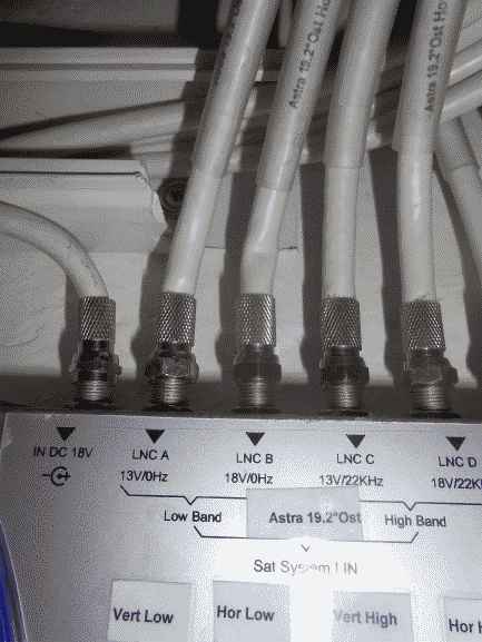
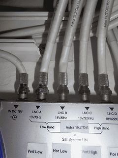
Anschlüsse eines Satellitenempfängers
Astra 19.2°Ost, IN DC 18V, LNC A 13V/0Hz, LNC B 18V/0Hz, LNC C 13V/22KHz, LNC D 18V/22KHz, Low Band, Astra 19.2°Ost, High Band, Sat System I IN, Vert Low, Hor Low, Vert High, Hor
-
Thread
Wie ich vor 40 Jahren ein eigenes "Canbus" baute
Ausgänge bleiben konstant. Dann kommt irgendwann mal ein kurzer Reset-Puls mit CLK100Hz mit ca. 200us HIGH. Die Breite ist nötig, damit der Reset an IC5 mit dem RC-Glied R6/C1 HIGH erreichen kann. Mit den kurzen 20kHz Pulsen vom Zählen passiert das nicht. Das ist der Trick. Wenn der CLK100Hz wieder auf LOW
Pull-Down Widerstände genutzt werden können, nur Pull-Up. Das ist auch ein historischer Grund für LOW aktive Signale wie #CS, #RD, #WR etc. Naja, eine witzige Schaltung aus der MC Gyver Kiste ;-)
-
Thread
Daten per Audio übertragen
Analyse. Es ist quasi wie morsen: * Carrier Frequency 3kHz * Modulation: ON/OFF Keying * Low: duration 50ms, 25ms ON, 25ms OFF * High: duration 100ms, 50ms ON, 50ms OFF Die durchschnittliche Bitrate wäre also ca. 14 Baud.
morsen: > * Carrier Frequency 3kHz Korrekt. > * Modulation: ON/OFF Keying Korrekt. > * Low: duration 50ms, 25ms ON, 25ms OFF > * High: duration 100ms, 50ms ON, 50ms OFF Das stimmt nicht ganz, was ich Dir neulich per PM geschickt hatte, war aber auch falsch, da hatte ich meine Aufzeichnungen
-
 Bild
Bild
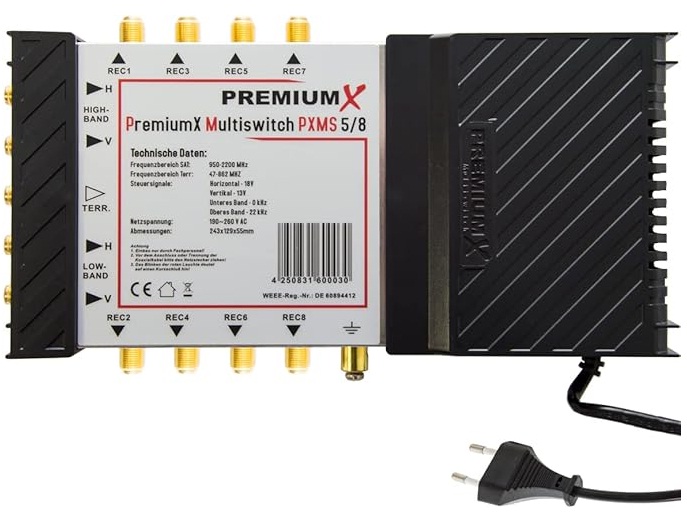
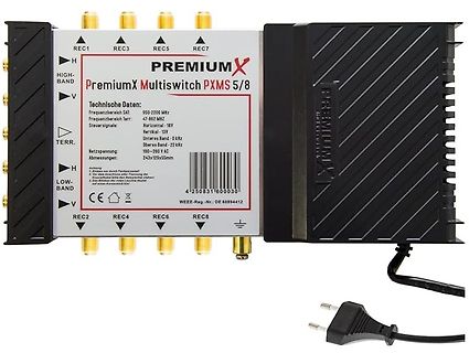
PremiumX Multiswitch PXMS 5/8
kHz Oberes Band: 22 kHz Netzspannung: 100-240 V AC Abmessungen: 243x129x55mm REC1 REC3 REC5 REC7 HIGH-BAND TERR. LOW-BAND REC2 REC4 REC6 REC8 4 250831 600030 WEEB-Reg.-Nr.: DE 60894412
-
 Bild
Bild
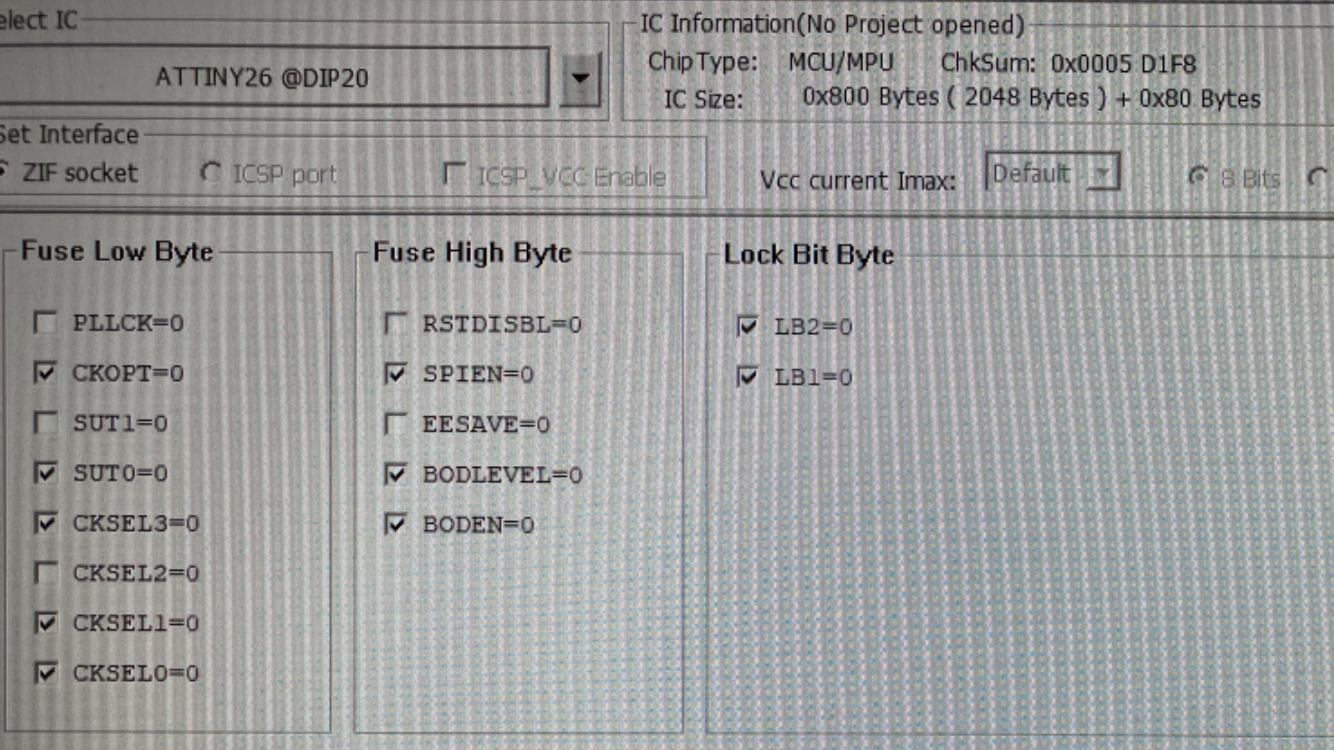
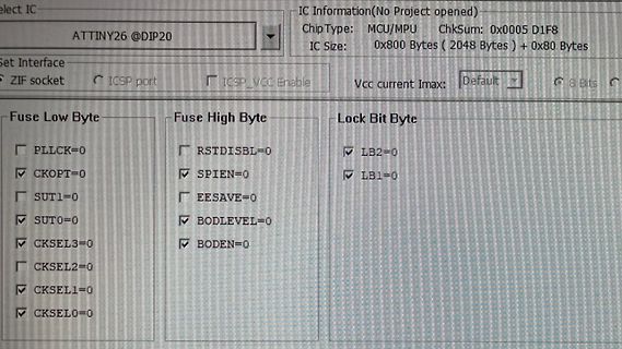
Software-Interface für AVR-Mikrocontroller-Konfiguration
0x80 Bytes Set Interface ZIF socket ICSP port ICSP_VCC Enable Vcc current Imax: Default 8 Bits Fuse Low Byte PLLCK=0 CKOPT=0 SUT1=0 SUT0=0 CKSEL3=0 CKSEL2=0 CKSEL1=0 CKSEL0=0 Fuse High Byte RSTDISBL=0 SPIEN=0 EESAVE=0 BODLEVEL=0 BODEN=0 Lock Bit Byte LB2=0 LB1=0
-
 Bild
Bild
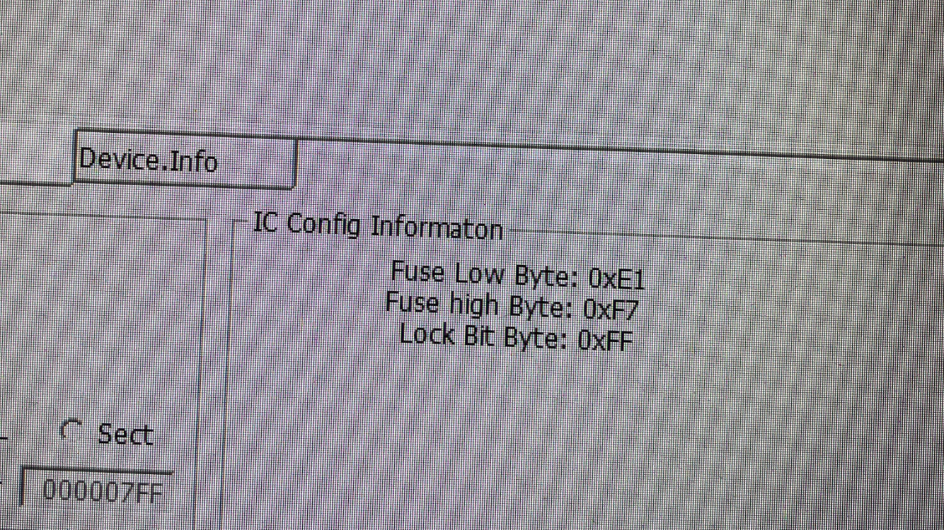
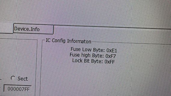
Software-Anzeige von IC-Konfigurationsdaten
Device.Info IC Config Informaton Fuse Low Byte: 0xE1 Fuse high Byte: 0xF7 Lock Bit Byte: 0xFF Sect 000007FF
-
Thread
Diagnose Satellitenfernsehen
der da. Sicher. Dafür ist er da, weil auf einem Koaxkabel nur einer der vier Betriebsmodi H/V High/Low laufen kann. Aber der LNB muss alle vier Modi gleichzeitig können und ist mit vier Kabeln am Multiswitch angeschlossen.
Erstmal *scheint* es kein Problem mit der Spannungsversorgung zu geben, wenn die H/V-Umschaltung im Low-Band grundsätzlich funktioniert, für die High/Low-Umschaltung ist das 22 kHz Signal zuständig. Wenn aber eines der High-Bänder funktioniert, *scheint* auch das 22 kHz Signal zu stimmen. VL: 14 V,
-
Thread
PC: das Zeitalter neuer Hardware
dass ich schon vor vielen Jahren weg von speziellen PCs fürs Programmieren gekommen bin. Also keine High-End Systeme wie man sie früher brauchte damit der Compiler in erträglicher Zeit fertig wurde. Der ganze Haushalt war über Jahre hinweg gut mit Supermarkt-PCs bedient. Auch ich für's Programmieren und
parameters on-device with blazing-fast speeds. It also includes the updated dual Micro NPU inside the ultra-low power Qualcomm® Sensing Hub for enhanced security, login experience and privacy, including the ability to wake the device when in sleep mode. Sensitive data can stay on your laptop for increased security
-
Thread
Renesas, Synaptics, GigaDevice und Espressif – Zertifikationen und neue MCUs
Function)*, CAN FD*, RSIP-E11A*, CTSU2SL, UART, I2C, SPI, 12-bit ADC, 8-bit DAC, Comparator, PWM timer, Low power timer • Operating range: 1.6V to 5.5V, -40°C to 85°C/105°C • Package Options: 48/64/80/100-pin LFQFP, 48-pin HWQFN • 5V power supply support: High noise immunity and dynamic range
MCUs are based on Renesas’ RXv3 CPU core, enabling 355CoreMark at 64MHz. This score is 2.5 times higher than competing 64-MHz class MCUs. Compared to other 64-MHz class MCUs, the RX261/RX260 also delivers 25 percent lower active current and 87 percent lower standby current. [/c] ### Renesas
-
 Bild
Bild
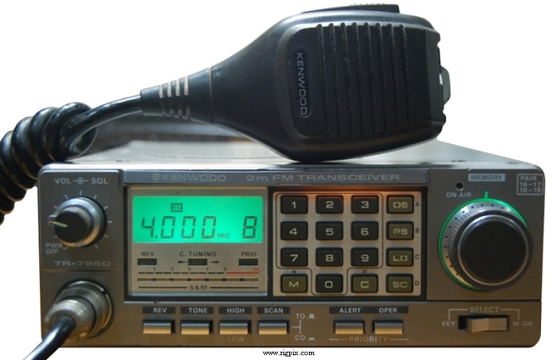
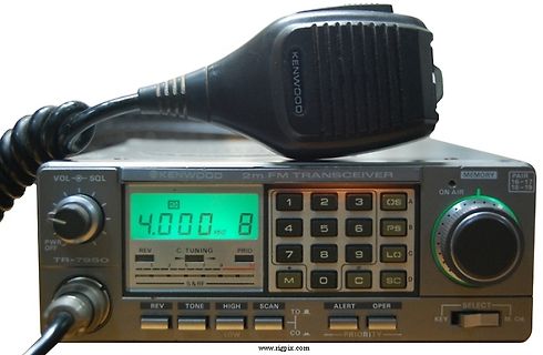
Kenwood TR-7950 Funktransceiver mit Handmikrofon
TRANSCEIVER MEMORY PAIR VOL-SQL 4.000 MHz ON AIR TR-7950 REV C. TUNING PRIO S&RF PS L SC D REV TONE HIGH SCAN TO ALERT OPER LOW PRIORITY KEY SELECT M. CH
-
 Bild
Bild
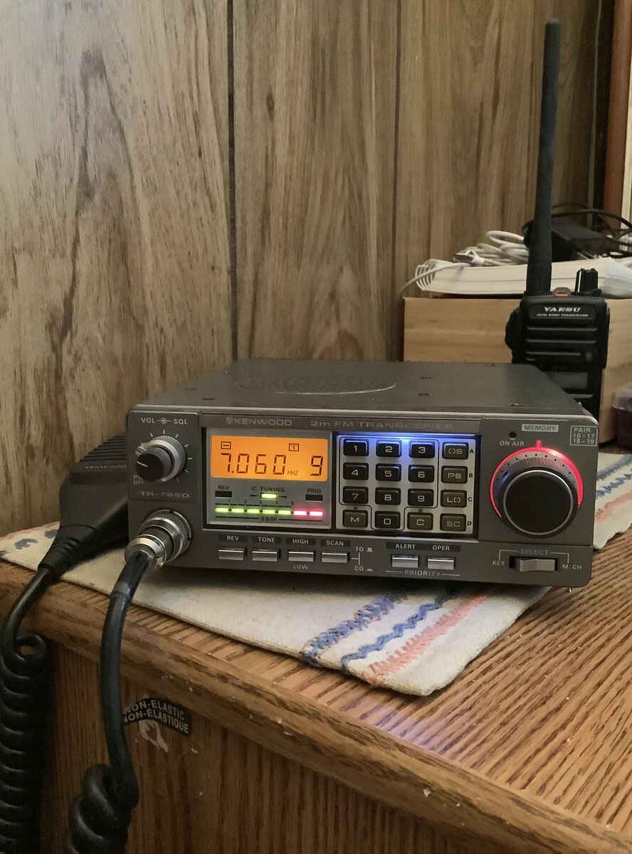
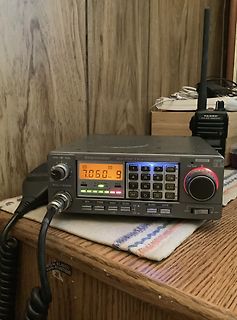
Kenwood TR-7950 Funkgerät
MEMORY PAIR 18-18 7.060 9 ON AIR 1 2 3 OS 4 5 6 PS B REV C TUNING PRIO 7 8 9 LO C M Q C D REV TONE HIGH SCAN ALERT OPER SELECT KEY M CH LOW CO PRIORITY
-
 Bild
Bild
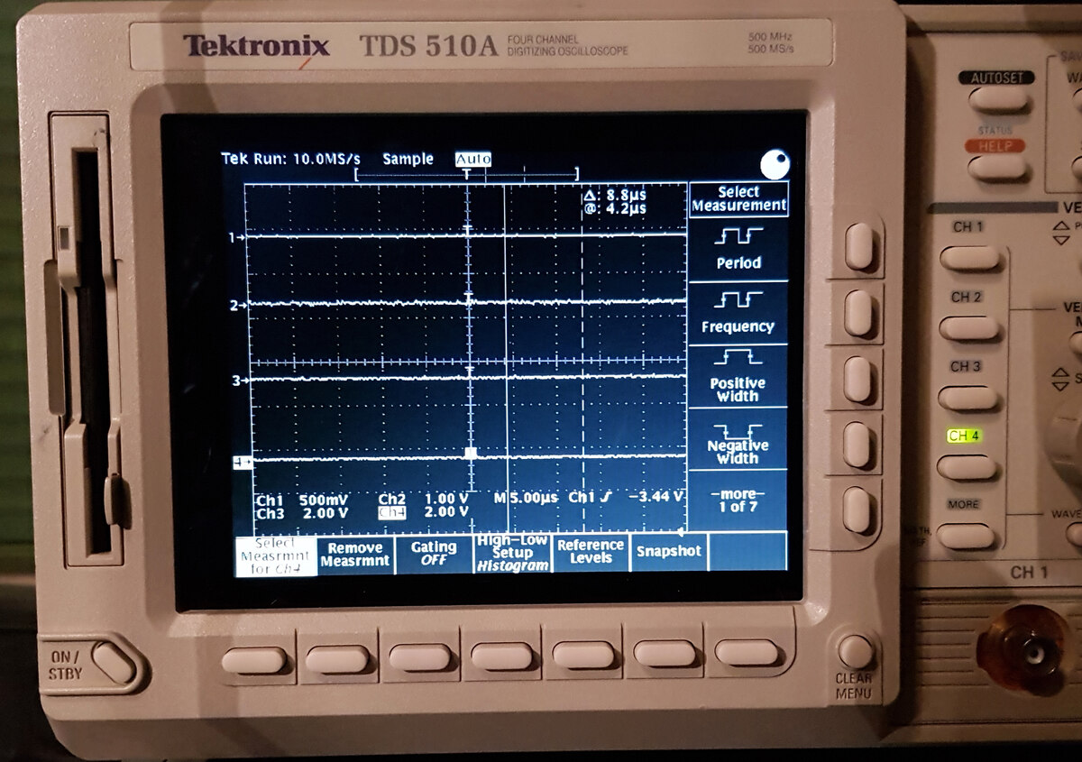
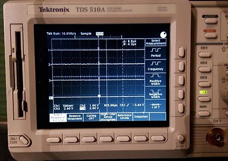
Tektronix TDS 510A Oszilloskop mit Messkurve
Ch4 2.00V M 5.00µs Ch1 ✓ -3.44V -more- 1 of 7 Select Measrmnt for Ch4 Remove Measrmnt Gating Off High-Low Setup Histogram Reference Levels Snapshot CLEAR MENU ON/STBY
-
 Bild
Bild
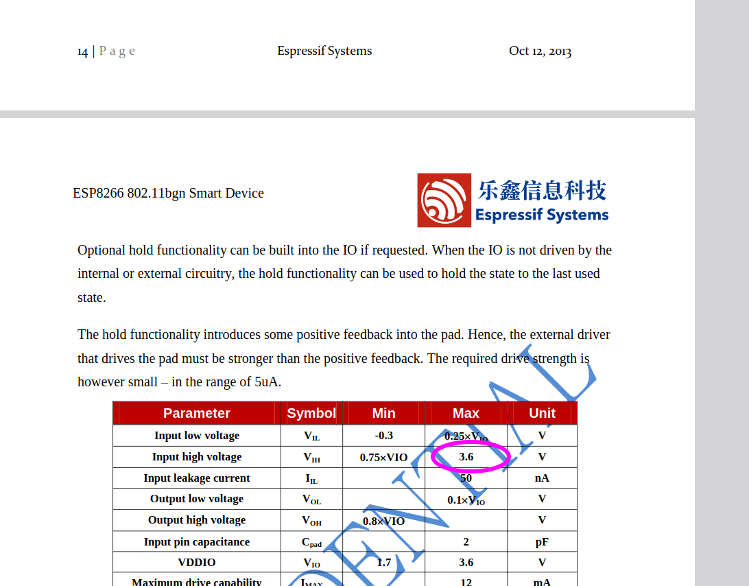
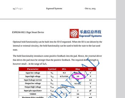
Ausschnitt eines ESP8266 Datenblatts mit Tabelle
required drive strength is however small – in the range of 5uA. Parameter Symbol Min Max Unit Input low voltage VIL -0.3 0.25xVIO V Input high voltage VIH 0.75xVIO 3.6 V Input leakage current IIL 50 nA Output low voltage VOL 0.1xVIO V Output high voltage VOH 0.8xVIO V Input pin capacitance Cpad 2 pF VDDIO
-
Thread
Zweifarbiges LED ansteuern
www.mikrocontroller.net/topic/572091#7760072 brauchbar wenn halt nicht die Spannungsschwellen wären, ab 1,6 high welcher HCT kann das? kommt mir unsicher vor, aber wer statt ein HCT Logikgatter einen NPN Transistor BC547 o.ä. setzt, der kommt mit 1,6V sicher durchgeschaltet auf low und mit 0V sicher auf high
einem Spannungsteiler der sogar den Strom getrennt einstellen kann für grün und rot, je nachdem ob high oder low aus der Transistorschaltung kommt. http://uploads.tapatalk-cdn.com/20160810/05fe28d20c84081ea0891496f0f2227d.png R1/R2 Transistoren LED R3/R4 Widerstaände
-
 Bild
Bild
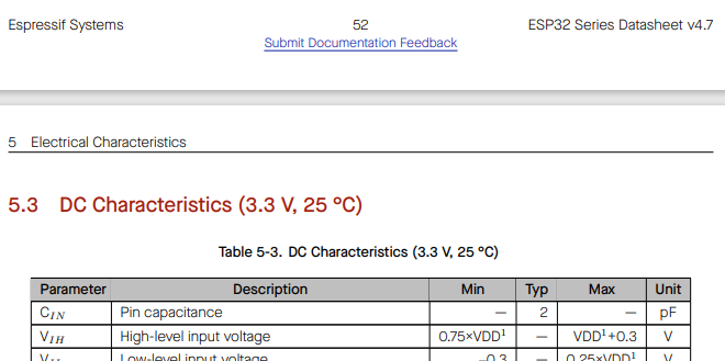
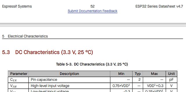
Ausschnitt aus einem ESP32 Datenblatt mit DC-Charakteristiken
Characteristics (3.3 V, 25 °C) Parameter Description Min Typ Max Unit CIN Pin capacitance – 2 pF VIH High-level input voltage 0.75xVDD1 – VDD1+0.3 V VIL Low-level input voltage – 0.3 V
-
Thread
Wer hat ein ILI9341 Display mit 5v im Betrieb?
verwendet werden kann kann. Lies doch bitte das Datenblatt. VDDI zwischen 1.65 und 3.3V Logic High Level Input Voltage zwischen 0.7*VDDI und VDDI Das impliziert, dass die Spannung an den digitalen Eingängen 3.3V nicht überschreiten darf. Mike K. schrieb im Beitrag #7758650: > Ich will keinen
ist es nicht. Siehe USB. Da ist für VBus 5V gewählt worden, obwohl der Signalpegel für D+ und D- bei Low- und Full-Speed bei max 3.3V liegt. Und warum? Klar, dadurch, dass VBus das USB Device versorgt, fließt dort ein nicht vernachlässigbarer Strom, und der führt zu einem Spannungsabfall. Also erhöht man
-
Thread
SPI Master mit Attiny1616
and NSS as output PORTC_DIRSET = 0x02; //set rst as output PORTC_OUTSET = 0x02; //set reset high SPI0_CTRLA = 0x23; SPI0_CTRLB = 0x04; } [/c] [c]void readReg(uint8_t reg, uint8_t *result, size_t length = 1) { uint8_t message[length + 1]; PORTA_OUTCLR = 0x10; _delay_ms(2);
PORTA_OUTSET = 0x10; } [/c] [c]void writeReg(uint8_t reg, uint8_t *data, size_t length = 1) { //pull cs low PORTA_OUTCLR = 0x10; _delay_ms(2); uint8_t message[length + 1]; message[0] = reg | 0x80; memcpy(&message[1], data, length); for (int i = 0; i < length + 1; i++) { SPI0_DATA =
-
Thread
High Side Shunt mit Spannungsteiler
Spannungsteiler]]. Die Ströme mit einem Shunt und passenden Stromverstärker. Die gibt es fertig als high side current sense amplifier. NEIN, mit einfachen Spannungsteilern geht das nicht. > Nun kann ich das per Low Side Shunt (Ayrton) machen, aber dann entsteht > eine große Loop zwischen Quelle und
zu lesen. Leicht verständlich und mit Beispielen: https://www.renesas.com/ja/document/apn/an1827-high-side-high-current-sensing-techniques
-
Thread
ESP8266 Wemos D1 mini DeepSleep issue
milliseconds = 30 seconds Serial.println("Loop is running..."); digitalWrite(LED_BUILTIN, LOW); // Turn the LED on (LOW is the voltage level because the LED is active LOW) delay(1000); // Wait for 1 second digitalWrite(LED_BUILTIN, HIGH); // Turn the LED off (HIGH voltage level turns it off) delay(1000); } digitalWrite(LED_BUILTIN, HIGH); Serial.print("Sleep"); // Send data over WiFi or to the cloud here (e.g., MQTT or HTTP request) // Sleep for 1 hour (1 hour = 3600e6 microseconds) ESP.deepSleep(10e6); }
-
Thread
L293 als 5V -> 12V LevelShifter?
keine 12V am Ausgang, da fehlt je nach Strom 1-2V, denn der hat bipolare Ausgangsstufen. Ebenso bei LOW, oder kommen 1-2V raus. Verkraftet das dein Bus? Wenn ja, ist der IC nutzbar.
Spec steht: Nachdem der Master (Regelung) seine Anfrage gesendet hat, setzt er den DL-Bus auf High (+12V mit max. 40mA). Nach einer Wartezeit von mindestens 20ms, sendet der Slave die angeforderten Daten (ohne SYNC). Nach erfolgter Antwort vom Slave und einer erneuten Wartezeit von 2ms, fährt der
-
 Bild
Bild
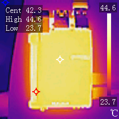
Wärmebild einer elektronischen Komponente
Cent 42.3 High 44.6 Low 23.7 44.6 23.7 °C

-
 Bild
Bild
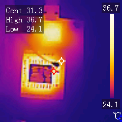
Wärmebild einer Leiterplatte
Cent 31.3 High 36.7 Low 24.1 36.7 24.1 °C

-
Thread
STM32H743 mit 32MByte externem SDRAM
Prescaler steht auf 1 ( div 2) also läuft es mit 120 MHz. Und die GPIO sind auf GPIO_SPEED_FREQ_VERY_HIGH initialisiert.
120 MHz, das ist mal wirklich zackig! Aber ich sehe gerade, daß bei mir die GPIO auf GPIO_SPEED_FREQ_LOW initialisiert sind. Das ist natürlich Quark. Danke nochmals, Axel
-
Thread
DC/DC Wandler / Step-down converter im low-current bereich
verdammt schlechten wirkunsgrad. Probiers mal damit: - https://www.google.com/search?q=stepdown+low+quiescent+current Evtl. kannst du ja noch ein "ultra" mit einfügen... ;-)
www.mikrocontroller.net/attachment/96118/stepdown.png Mit solche Transistoren 2SD2537 NPN, SOT-89, 25V 1.2A, High hFE Transistor 2SB1427 PNP, SOT-89, -20V -2A, High hFE Transistor Würden diskret über 80% erreicht werden.
-
Thread
Altera USB Blaster III
ADBUS1 TDI ADBUS2 TDO ADBUS3 TMS ADBUS4 NTRST ADBUS6 PROC_RST ACBUS7 BLUE (RGB LED Active LOW) ACBUS6 GREEN ACBUS5 RED ACBUS4 ENABLE, high when JTAG active
-
Thread
Arduino Nano, P-MOSFET & DC-DC StepUp für BobbyCar LEDs
D13 geht per Programmcode dann auf LOW.
Zustand zu halten. Christian K. schrieb im Beitrag #7755985: > D13 geht per Programmcode dann auf LOW. Interessanter ist AUS, dann muß D13 high sein. Das kannst Du nicht gewährleisten, also Mist: Loco M. schrieb im Beitrag #7756148: > Über R2 und R3 liegen im ausgeschalteten Zustand 4V an D13
-
Thread
Gleichtaktstörung zerstört eure Elektronik! Grund: Schaltnetzteile ohne Erdung.
macht, sehen das nur ein ganz paar Leute. Weil kompliziert ist, man nachdenken muss, nur mit teurem high end Gedöhns messen kann und der Normalo CM Störungen maximal als schlechten Radioempfang kennt, wenn er denn überhaupt jemals damit in Berührung gekommen ist. Wenn Bernd Blindfisch Bullshitbingo
Aufgefallen ist mir das übrigens, weil ich diese Schaltung auch über ein JouleScope versorge hatte - weil low-power Anwendung mit kleinem Akku. Ein paar 100µA mehr Versorgungsstrom war da schon ziemlich auffällig.... Peter D. schrieb im Beitrag #7756930: > > Es ist aber schon ein deutlicher Unterschied