außen so zusammengelegt wurden, dass das nicht mehr geht. Beim Trotec Lokales Klimagerät PAC 2015 E geht es zum Beispiel noch. Bei vielen Zweischlauchgeräten steht nicht verfügbar: https://www.amazon.de/Sichler-Exclusive-Klimager%C3%A4t-mobil-Monoblock-Klimaanlage/dp/B088TQ331G
problemlos um 15° C Grad > runter. Das Ding gab es vor zwei Jahren für € 199,- auf eBay.
CURRENT (mAdc) Figure 1. Normalized DC Current Gain Figure 2. “Saturation” and “On” Voltages 2.0 1.0 V C E TA= 25°C / -55°C to +125°C G m 1.2 L 1.6 T O N V C = 200 mA C 1.6 E F I 1.2 E M C = IC= C = 50 mA C = 100 mA C 2.0 - 10 mA 20 mA E O 0.8 U C A 2.4 E R O P , 0.4 E 2.8 E , VC V θ 00.02 0.1 1.0 10 20 0.2
pinout are supported, depending on the cabling and adapters included with the particular kit. Figure 4-2. SAM JTAG Header Pinout 1 2 VCC TMS GND TCK GND TDO (KEY) TDI GND nRESET SAM JTAG Table 4-1. SAM JTAG Pin Description Name Pin Description TCK 4 Test Clock (clock signal from the Atmel-ICE into the
...........................................................11 4.2. Port E Data Direction Register................................................................................................... 12 4.3. Port E Data Register......................................
Enable STB Data Latch CE# Output Enable OE# Logic Y-Decoder Y-Gating STB V Detector Timer t CC a L e X-Decoder Cell Matrix d A0–A18 d A 4 Am29F040B 21445E8 November 11, 2009 D A T A S H E E T CONNECTION DIAGRAMS 2 5 6 8 C E 7 A A A A V W A 1 4 3 2 1 32 31 30 A7 5 29 A14 A6 6 28 A13 A5 7 27 A8 A4 8 26
sogenannte "PULSAM" PWM Modulator des Senders. https://www.bbceng.info/Technical%20Reviews/tott/31-33_G4OYX_Signal_Issue_41.pdf
Radio 4 Longwave will NOT go quiet at the end of June, BBC suggests: https://keeplongwave.co.uk/2025/06/16/radio-4-longwave-will-not-go-quiet-at-the-end-of-june-bbc-suggests/ "Listeners may have noticed that
volts and up to 12 volts. 2. Scheme and function For those interested Amplifier 7,6 V Mixer 8,2 V R4 D1 J2 Dr1 R3 L2 C2 Audio R1 6,6 V Dr2 amplifier L1 C1 J1 C4 7,6V C5 P1 IC1 C9 L3 C3 Q1 Q2 C6 386 0,25 V J4 R2 C7 C8 J3 a C11 D2 C10 R7 R5 IC2 555 b P2 5,1 V 0,8 kHz 0,8 kHz R6 kHz Local oscillator 16,4
Zeitachse scheint sich ein Muster zu wiederholen. Das klingt stark nach DSSS. Vielleicht IEEE 802.15.4 ?
verschlüsselt, aber etwas Sinnvolles rauslesen kann ich jetzt direkt trotzdem nicht: [code] aaaaaaaaaa 2dd4 5c323793bc8000f73d001e425fa4aeefc140687357908f0e302ec2e856cc74000007b8aa27e8a158051d57b7a46fd002a800001750000000281a05c1b02626078739b3f2c71111 aaaaaaaaaa 2dd4 ac210082bc81000000000000000000000000000000000000000000000000000000000000000000000000000000000000000000000000000000000000000003b3a60e031a98489eb5b69a6ecc532e24e544001001
and wiring capacitances R, resistor is for threshold shifting. Figure 3. Switching Response Figure 4. Response Control Node http://onsemi.com 4 MC1489, MC1489A TYPICAL CHARACTERISTICS (V CC = 5.0 Vdc, TA= +25°C, unless otherwise noted) 10 6.0 8.0 5.0 VI E A 6.0 c O ( 4.0 ( 4.0 RT RT R T RT N E 5.0 k
dedizierter Ethernethardware ante Portas stehen. ### PicoScope: preiswerte Einstiegsmodelle in die 3000E-Serie. Nun gibt es eine aktualisierte Variante der 3000E-Serie, die mit einer Bandbreite von nur 100 bzw. 200 MHz auftritt. Lohn der Mühen ist eine Senkung der Kosten für das PC-Oszilloskop: Die 100
verwendet AMS Osram folgendes über das Produkt: [c] Designed to drive up to 9 LEDs with precise 16-bit PWM dimming, the AS1163 enables vibrant, customizable lighting experiences. Its daisy-chain capability, slim PCB support, and full compatibility with the OSIRE E3731i via the Open System Protocol
SMT Full-color TOP LED Waterclear” product group. The new RGB LEDs in their respective packages PLCC4 2121, PLCC4 3528 and PLCC6 3528 are characterized by excellent heat resistance. Their insensitivity to temperatures from -40 to +100 °C makes them ideal solutions for reliable, color-variable lighting
AM6254 as found in the BeaglePlay SBC • CPU ◦ Quad-core 64-bit Arm Cortex-A53 @ 1.4 GHz ◦ Arm Cortex-M4F real-time core @ 400 MHz with 256KB SRAM • GPU – Imagination PowerVR Rogue AXE-1-16M with support for OpenGL 3.x/2.0/1.1, Vulkan 1.2 [/c]  Self-limited A V 7 Maximum pin voltage (Ipin ≤ 1 mA) Self-limited V LINEmax I 4 Maximum source current 2 mA RFmin 1 to 6, 8 Analog inputs and outputs -0.3 to 5 V Note: ESD immunity for pins 14, 15 and 16 is guaranteed up to 900 V 4.2 Thermal data Table 4. Thermal data Symbol Description
TEMPERATURE (°C) TJ, JUNCTION TEMPERATURE (°C) Figure 17. High−Voltage Current Source vs. Figure 18. Pin 16 Leakage Current vs. Temperature (@ V CC = 0 V) Temperature (@ V PIN16 = 500 V and VCC = 16 V) www.onsemi.com 9 NCP1605, NCP1605A, NCP1605B 24 −12 22 −14 ) m ) , 20 m −16 E , R K U 18 I −18 O _ _ E E
outline HSOP44: plastic, heatsink small outline package; 44 leads; low stand-off height SOT1131-1 E A D x c y E2 X H E v A D1 D2 1 22 pin 1 index Q A E 1 A2 (A3) A 4 θ Lp detail X 44 23 w Z e bp y Z θ 1.30 8° 0.07 1.13 4° 0 5 10 mm 0.95 0° Dimensions scale Unit A A A A b c D (1) D D E (1) E E e H L Q v w x 2 3 4 p 1 2 1 2 E p max 3.5 3.5 +0.08 0.38 0.32 16.0 13.0 1.10 11.1 6.2 2.9 14.5 1.10 1.7 mm nom 3.3 0.35 +0.02 0.30 0.25 15.9 12.8 1.00 11.0 6.0 2.7 0.65 14.2 0.91 1.6 0.25 0.12 0.03 min 3.2 −0.04 0.25 0.23
ON-RESISTANCE SWITCH ON-RESISTANCE vs vs JUNCTION TEMPERATURE SUPPLY VOLTAGE 180 120 115 TPS2112A 160 m W - - e e 110 n c t 140 t i TPS2112A i 105 e s R R n 120 n 100 - - c h i i 95 w 100 w - TPS2113A S n -) ( ( 90 D D r 80 r 85 TPS2113A 60 80 -50 0 50 100 150 2 3 4 5 6 TJ- Junction Temperature - C° VI(INx) Supply
AUGUST 2020 7.6 Typical Characteristics 320 260 312 304 240 A A ( 296 ( n n r 288 r 220 u 280 u t t e 272 e 200 s s u 264 u Q -40qC Q -40qC 256 25qC 180 25qC 248 85qC 85qC 125qC 125qC 240 160 2 4 6 8 10 12 14 16 18 20 22 2 4 6 8 10 12 14 16 18 20 22 Input Voltage (V) D001 Input Voltage (V) D002 ILM =
SWITCH ON-RESISTANCE vs vs JUNCTION TEMPERATURE SUPPLY VOLTAGE 180 120 W 115 TPS2114A W 160 m - - e c 110 n TPS2114A n t 140 s i s 105 e e - n n 120 O 100 h h t i w TPS2115A w 95 S 100 S -) -) n o 90 ( S D 80 rD TPS2115A r 85 60 80 -50 0 50 100 150 2 3 4 5 6 TJ- Junction Temperature -°C V - Supply
. Tweaking C2 value to compensate the mismatch introduced by the notch filter To VR_PA F n p 7 6 H 4 = n Equivalent 9 1 4 C2= 2.52 pF C C = circuit 2 L C OUT= 144 pF L1= 4.45 nH Ω 2 RFO_HP F L2= 3.4 nH 5 or RFO_LP 3 1 . T 5 O =1 R C Note: The same procedure can be done to the value of L1 (starting with
Hans schrieb im Beitrag #7884149: > Ah der schon KI 4.0 Sowas wird als Plus gegenueber LiMux verkauft.
einfach abnicken sollte: https://filestore.community.support.microsoft.com/api/images/2acfe200-c0b1-4d12-80dc-fd5e50623358?upload=true Alexander schrieb im Beitrag #7885164: > Wenn Du dich als Windows 10 oder 11 Nutzer outest, klicke mal bitte in > das Suchfeld in der Taskleiste Das Suchfeld
shields. w e 2 Dual voltage options are not available with r L or Z Filter Types E 3 When using the interconnection block, the last n 3 digits of the part number are BX (0, A, or B) r y Optional switch 4 High performance
definitely OFF at E e/R ≤ 20 µW/cm² (OFF = MARK (quiescent state) = Binary 1) IEC 732/02 Figure 6 – Test arrangement for the receiver 62056-21 IEC:2002 – 33 – 4.3.5.4 Environmental lighting condition The optical path
l o d o 1 s r T 0.5 0 2.7 4.0 5.0 Vcc Figure 75. I/O Pin Input Hysteresis vs. V CC I/O PIN INPUT HYSTERESIS vs.V cc TA= 25 C 0.18 0.16 ) 0.14 ( i 0.12 e t y 0.1 h u 0.08 I 0.06 0.04 0.02 0 2.7 4.0 5.0 Vcc 83 0839I–AVR–06/02 Register Summary Address Name Bit 7 Bit 6 Bit 5 Bit 4 Bit 3 Bit 2 Bit 1 Bit 0 Page $3F ($5F) SREG I T H S V N Z C page 16 $3E ($5E) Reserved $3D ($5D) SPL SP7 SP6 SP5 SP4 SP3 SP2 SP1 SP0 page 17 $3C ($5C) Reserved $3B ($5B) GIMSK INT1 INT0 – – – – – – page
prüfen Akku (4) auf, wenn nur noch die rote Die Ladezustandsan- LED der Ladezustands- zeige (3) signalisiert anzeige (3) leuchtet. den Ladezustand des Akkus (4). Während des La- devorgangs wird 16 DE AT CH der Ladestatus
operational. To assure a noise margin, the MOS-FET’s should have a minimum threshold voltage V of e.g. 0.4V and VDD1 must stay below this value. The isolation feature can also be applied if no level shifting is required, VDD1 and VDD2 may have the same value, e.g. both 3.3V or both 5V. 11 Philips Semiconductors
order. The minimum magnitudes shown shall be replaced by implementation-defined magnitudes with the same sign. The values shall all be constant expressions suitable for use in #if preprocessing directives. The components are described further in 5.2.4.2.1. #define CHAR_BIT 8 #define CHAR_MAX UCHAR_MAX
E O O SPICS1 I I D0/A0/Qt1 IO1 3 3 S S CS D1/A1/Qt2 IO2 ESP32-S3 IO47 DVP_HREF D2/A2/Qt3 IO3 IO48 DVP_Y9 CAM D3/A3/Qt6 IO6 D4/A4/SDA/Qt4 IO4 D5/A5/SDA/Qt5 IO5 VDD_SPI y e XIAO Header SPI D External a -
3.00±0.1V 200±30mV -210±30mV available E HY2120-MB 4.45±0.025V 4.25±0.05V 2.25±0.08V 2.95±0.1V 200±30mV -210±30mV available A HY2120-NB 4.28±0.025V 4.08±0.05V 2.80±0.08V 3.00±0.1V 200±30mV -210±30mV available B HY2120-OB 4.25±0.025V 4.05±0.05V
Response time : (NOTE 3) Viewing angle AMPIRE CO., LTD. 6 6 BLOCK DIAGRAM & INTERFACE COM LCD Panel 1-16 20*2 Chars E RS R/W DB0~DB7 SED1278 SEG 1-40 E -1 S 4 VDD Driver VSS D, M, CL1, CL2 No. Symbol Function 1 VSS Ground (0V) 2 VDD Supply Voltage for Logic (+5V or +3.3V) 3 VO Contrast Adjustment 4 RS Data
Ich bin gespannt! Wie schaut es mit der Unterstützung der ATTiny4/5/9/10 aus? Da hätte ich das ein oder andere Projekt, bei dem das super nützlich wäre!
series-best-class-power-consumption-and-extended-temperature Die neue Variante erweitert dabei den bekannten RA0 E1 um mehr Interface-Möglichkeiten, und behält dabei - unter anderem - die 5 V-Fähigkeit: [c] RA0E2 MCUs are fully compatible with RA0E1 devices, offering pin-expansion while maintaining the same peripherals
protection • Packages: 32- and 48-lead QFNs, 32-, 48-, and 64-pin LQFP [/c] Mit dem FPB-RA0E2 steht außerdem ein Evaluationsboard zur Verfügung, das Entwicklern beim Spin-up von Designs helfen soll. ### ESP-HDMI-Bridge – HDMI-Ausgang für den ESP32-P4 Entwicklerkits für den ESP32-P4 weisen
operations, ×10EIBULL) 3.-(1) Operate time including bounce time 3.-(2) Operate time including bounce time 4. Release time including bounce time (Single (Single side stable) (2 coil latching) side stable) 3.0 3.0 3.0 2.5 2.5 2.5 s s s m m , e2.0 e 2.0 e2.0 t i t e e e r1.5 r 1.5 a p e e1.5 O O R Max. 1.0 1.0
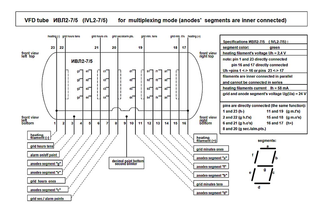
right top
Specifications ИВЛ2-7/5 (IVL2-7/5):
segment color: green
heating filament's voltage Uh = 2,4 V
note: pin 1 and 23 directly connected
pin 16 and 17 directly connected
Uh = pins 1 <-> 16 or pins 23 <-> 17
filaments are inner connected in parallel
and cannot be connected in series
heating currents Ih = 58 mA
grid and anode's voltage Ug(Aa) = 24 V
pins are directly connected (the same function):
1 and 23 (h-)
2 and 22 (g h.t's)
11 and 19 (g m.t's)
15 and 18 (g m.o's)
6 and 21 (h.o's)
16 and 17 (h+)
front view left bottom
front view right bottom
heating filament (-)
grid hours tens
Electronic units (voltages & code numbers) Compressors t 0 0 1 d C 0 C 0 r C 0 d C 0 I C 0 r C 0 C C 0 e & A i C 0 0 8 0 5 0 2 R134a Code a D 2 I D 2 t D 2 p D 2 E D 3 t D 3 a D 4 a D 4 n D 0 5 o D 6 6 x D 0 N x D 0 7 D 7 o D 7 o D 7 R404A/R507 * numbers n 4 N E 4 N h 4 N S 4 N O 4 N E h 4 N o 0 N o 5 N
keine Graphik, mir würde ein numerische Anzeige mit 2..4 Zeilen reichen. Kennt vielleicht jemand zufällig eine (E-paper) Anzeige, die man einfach irgendwie seriell ansprechen kann ? Danke für sachdienliche Hinweise.
Display ist das wegen der Portrait Ausrichtung nicht geeignet und 2x16 oder 4x16 Zeichen bekommt man da schon gar nicht drauf angezeigt.

 Bild
Bild