100 100 100 90 90 90 80 80 80 P o 70 70 70 w 60 60 60 50 50 50 e 40 40 40 r 30 30 30 I n 20 20 20 l 10 10 10 e 0 0.1 1 10 30 0 0.1 1 10 30 0 0.1 1 10 30 t Frequency in MHz Frequency in MHz Frequency in MHz F i l e L Models r s 6A 10A & db db 100 100 P 90 90 o 80 80 w 70 70 60 60 e r 50 50 E 40 40 n 30 30 20 20 r 10 10 y 00.01 0.1 1 10 30 00.01 0.1 1 10 30 M Frequency in MHz Frequency in MHz o d Z Models u l e s 6A 10A db db 100 100 90 90 80 80 70 70
F10 when the monitor light turns green to access the utility. You can also press Esc to a menu that allows you to access different options available at startup, including the Computer Setup utility. NOTE: If you do not press F10 at the appropriate time, you must restart
Zusätzlich muß die Interrupttabelle angepaßt werden auf den "neuen" µC. beispielsweise sieht diese beim At13 so aus: If the program never enables an interrupt source, the Interrupt Vectors are not used, and regular program code can be placed at these locations. The most typical and general program setup
the Clock Select (CLKSEL) bit field in the Control A (TCBn.CTRLA) register. * 4.The counter value can be read from the Count (TCBn.CNT) register. The peripheral will generate a CAPT interrupt and event when the CNT value reaches TOP. * 4.1. If the Compare/Capture register is modified to a value lower than the current CNT, the peripheral will count to MAX and wrap around. * 4.2.At MAX, an OVF interrupt and event will be generated.
Interface address match, an external > level interrupt on INT0 or INT1, or a pin change interrupt can wake up > the MCU." Aber nur beim AT90S2313, ATTiny2313A. Beim ATmega328P fehlt diese Einschränkung und deshalb funktioniert der Code dort. Siehe obige Table 10-1 aus dem Datenblatt.
unter welchen Bedingungen. Dass ein INT0 oder INT1 die CPU aufwecken kann, ist wiederum auch beim AT90S2313 der Fall.
the T-bit as source and destination for the operated bit. A bit from a register in the Register File can be cop- ied into T by the BST instruction, and a bit in T can be copied into a bit in a register in the Register File by the BLD instruction. 16 AT90S2313 0839I–AVR–06/02 AT90S2313 Bit 5 – H: Half-carry
this, select the and total runtime of the „Overheated Alarm battery. Switch“ fjeld. • - Settings You can illuminate You will fjnd the at the battery’s charge the top right after you level indicator using have selected the bat- the „Battery identifj- tery. 48 GB MT Press the icon again The battery can also
the RX buffers per the datasheet instructions. We found out the hard way that the register involved can also return 0, and requires a flush of the RX buffers to regain functionality. The issue occurs seemingly randomly, on a perfectly working device, it can take months, weeks, days or hours. I don't
über eine gute Auftragslage berichtet: [c] "Infineon has performed well in the second quarter. Even at a more unfavorable exchange rate of $1.125 to the euro, we would be right on track and in line with our previous expectations for the fiscal year. Given that order intake still shows no signs at all
circuit either not working or “playing up” on too low a current range – that’s the burden voltage at work, starving your circuit of the voltage it needs to function correctly. You usually have no option but to reluctantly switch to a higher current range to lessen the effect. The problem can also be
Human Body Model) 4000 V Note: 5. Stresses greater than those listed under Absolute Maximum Ratings can cause permanent damage to the device. These are stress ratings only, and functional operation of the device at these or any other conditions beyond those indicated under Recommended Operating Conditions
Battery Before using this feature, the UPS must have been powered by utility power with output enabled at least once. Battery start can be disabled. See the "Cold start" setting in "ON/OFF Settings" on page 11. To start the UPS on battery: 1. Press the button on the UPS front panel until the UPS front panel
exceed overcharge delay time (T OC) an external charge control Nch MOSFET turns off with OC pin being at "L" level. The overcharge status can be release by the following two cases: (1) The voltage of the battery cell1 and the voltage of the battery cell2 are equal to or lowers than the overcharge release
pneumatic power unit together with product specific “quick change” tooling packs. The insertion heads can be equipped with a rotary insertion finger that can apply products at different angles without decreasing the insertion rate. The tooling packs can be exchanged within 30 minutes to meet your full range
built-in DC/DC converter.) (6) Normal / Extended temperature type. (7) Excellent LC : VOP maintains at 5V for whole temp. range, no need extra temp. compensation circuit. 2 NUMBERING SYSTEM AC-202A _ _ _ _ - _ 1 2 3 4 5 No Code Value Description Remark 1 G STN gray type LCD LCD Type Y STN yellow green
VCC VCC input input/output 1 K 1 K GND GND SCD5580/5581/5582/5583/5584 2–3 Optical Characteristics at 25°C VCC =5.0 V at 100% Brightness Level, Viewing Angle: X Axis 55°,Y Axis 65° Red SCD5580 Description Symbol Min. Typ. Units Luminous Intensity IV 36 90 cd/dot Peak Wavelength PEAK 665 nm Dominant Wavelength
and stored in a Capacity remaining rate Storage Characteristics temperature-controlled environment at 25ºC ± ≥ 90% (C in 2.1) min 2ºC for 30 days. After storage, cells shall be discharged per 4.1.2 to obtain the remaining capacity*. 4.3.2 Cells shall be charged per 4.1.1 and stored in a No leakage, High
IO-Link remains stable and has been growing continually for years, with more than 61 million nodes at last count. IO-Link continues to successfully establish itself as a global standard. PROFIsafe This kind of trend can also be seen with PROFIsafe nodes. Following exceptional growth in the preceding
Ñ Switcher optimized for off-line flyback converter no load or light load condition. The switchted at ‘Extended burst mode’ control greatly reduces the improve the conversion efficiency. At light load or easily to meet the international power conservation mode threshold level and device enters Burst
BD35F-HD and BD1.4F-VSD-HD are new versions the need for current batteries if an ice bank is used which can handle extreme vibrations. for energy storage.When storing the sun energy in ice packs the cabinet can be kept at desired BD35F-B (Bus-optimized) temperatures both night and day. The BD35F-B is a special
respect to network ground terminal. 2. All typical values are =5V,eTA= + 25°C. 3. Test each pin one at a time, 5. Measured with V'L applieCEtand logic high at the outpul.output under test is at low logic level. Output sink current is supplied through a resistor to Vee. 6. Measured with V'H applieCE.o
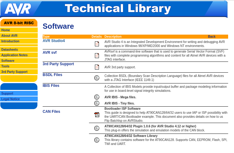
3rd Party Support
Support
Legal Notice
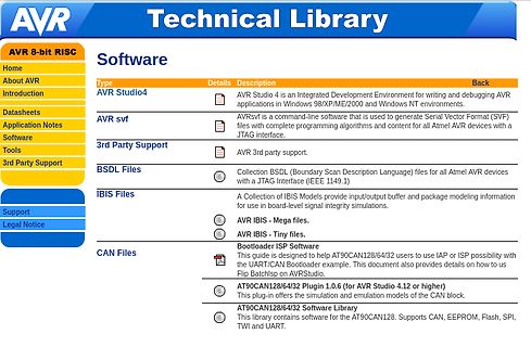
AVR Studio4
AVR svf
3rd Party Support
BSDL Files
iBIS Files
CAN Files
AVR 3rd party support.
Collection BSDL files for all Atmel AVR devices with a JTAG interface (IEEE 1149.1)
A Collection of IBIS Models
AVR IBIS - Mega files.
AVR IBIS - Tiny files.
Bootloader ISP Software
AT90CAN128/64/32 Software Library
connects the pin to the VIO voltage. Open-drain outputs are typically used when interfacing to logic at a higher voltage than the VIO pin. These pins can be safely pulled to the higher, external voltage through an external pull-up resistor. The maximum external pull-up voltage is 5 V. The speed of reading
clock frequency as described in the General Operating Ratings section. The system clock prescaler can be changed back after the oscillator calibration value has been updated. OSC20M Stored Frequency Error Compensation This oscillator can operate at multiple frequencies, selected by the value of the
Hallo, ich bin auf der Suche nach einer Fassung für den AT90CAN128. So, wie die hier https://www.reichelt.de/de/de/shop/produkt/ic-fassung_68-polig_plcc-14703 Allerdings in 64-polig. Bei meiner Suche finde ich nur 68-polig. Weiss jemand, wo ich die
Den AT90CAN128 gibt es auch im QFN-Gehäuse. Die sind deutlich stabiler, also müssten die Sockel eigentlich einfacher sein. Naja, Textool hat 2 verschiedene für 0.4mm-Pitch und scheinbar keinen für 0.5mm. Muss
possible performance. The the device is controlled by a separate logic input, DMOS output transistors can operate at supply while a common enable controls both channels. voltages up to 42V and efficiently at high switch- The I.C. is mounted in three different packages. BLOCK DIAGRAM July 1997 1/20 This
connects the pin to the VIO voltage. Open-drain outputs are typically used when interfacing to logic at a higher voltage than the VIO pin. These pins can be safely pulled to the higher, external voltage through an external pull-up resistor. The maximum external pull-up voltage is 5 V. The speed of reading
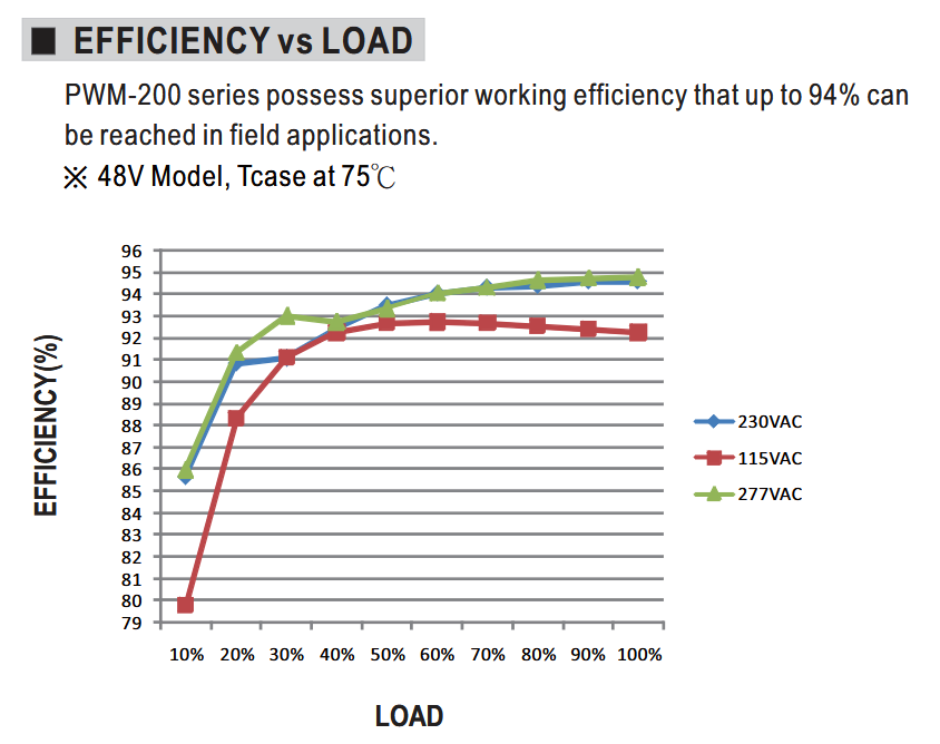
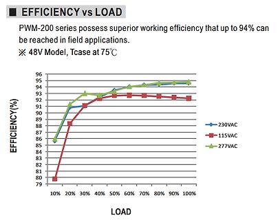
EFFICIENCY vs LOAD
PWM-200 series possess superior working efficiency that up to 94% can be reached in field applications.
※ 48V Model, Tcase at 75°C
EFFICIENCY(%)
LOAD
230VAC
115VAC
277VAC
10% 20% 30% 40% 50% 60% 70% 80% 90% 100%
CARD_POWER 1 G N D 20 FG1 DIR G LOW = Power OFF FG2 TC74VHCT245AFT SCAB1A8100 R255 1 IC94B 100k HD74LV32AT D IC90C IC90D RPC05T@J D 5 CARD_XBUSEN HD74LV00AT HD74LV00AT XCARD_BUS_ENABLE 6 RPC05T@J 9 12 XCA_IOIS16 4 R254 22 8 11 XIOIS16 10 13 RPC05T@J R256 NIU D +5 D +3.3 D LTLXBIG LTLXBIG R257 0 R258 NIU R259
5.9 13.0 9.0 7.7 15.0 13.8 11.2 15.0 15.0 13.7 (A) Peak Current (A) 63.5 30.1 24.9 89.0 44.9 37.0 90.0 64.0 54.1 90.0 73.7 58.9 Don’t see exactly what you need? Optional: Tachometer Specifications Still need help? Have ElectroCraft build you a Model Easily build your own motor at Tach Resistance Tach
Powering the Target These are configuration essentials: • When using the USB connection, PICkit 3 can be powered from the PC but it can only provide a limited amount of current, up to 30 mA, at VDD from 1.8-5V to a small target board. • The desired method is for the target to provide VDD since it can provide a higher current. The additional benefit is that plug-and-play target detection facility is inherited, i.e., MPLAB IDE will let you know in the Output window when it has detected the target
the forward converter works at the pre-regulated intermediate circuit voltage. This means that a higher transformer ratio can be selected, reducing the current load for the MOSFET. Furthermore, a larger duty cycle can be set during
/K ± 1.0 % UB C1 51R1 = 51.1 Ω MBE/SMA 0414 ± 2.0 % L0 RP ± 5.0 % KL R2 R4 N4 Notes • The products can be ordered using either the PRODUCT DESCRIPTION or the PART NUMBER. • Standard products are not CECC approved. • Radial version (RB,UB) cannot be qualified according to CECC so these can only be ordered
CARD_POWER G N D FG1 1 DIR G LOW = Power OFF 20 FG2 0 TC74VHCT245AFT SCAB1A8100 R255 1 IC94B 100k HD74LV32AT D IC90C IC90D RPC05T@J D 5 CARD_XBUSEN HD74LV00AT HD74LV00AT XCARD_BUS_ENABLE 6 RPC05T@J 9 12 XCA_IOIS16 4 R254 22 8 11 XIOIS16 10 13 RPC05T@J R256 NIU D +5 D +3.3 D LTLXBIG LTLXBIG R257 0 R258 NIU R259
addition, there is a user range. User write to the memory is restricted to the NVM User Range. User read can also be performed to the other NVM addresses. 4.8.1 NVM User Range The host can write and read the memory of the user range. The range is located at addresses 0x20-0x22. Each address holds 2 bytes.
is enabled with ACC_CONF.acc_perf_mode=0b1. In this power mode, the accelerometer data is sampled at equidistant points in the time, defined by the accelerometer output data rate parameter ACC_CONF.acc_odr. The output data rate can be configured in one of eight different valid ODR configurations going
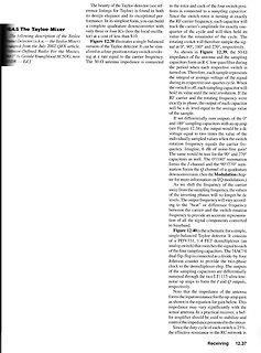
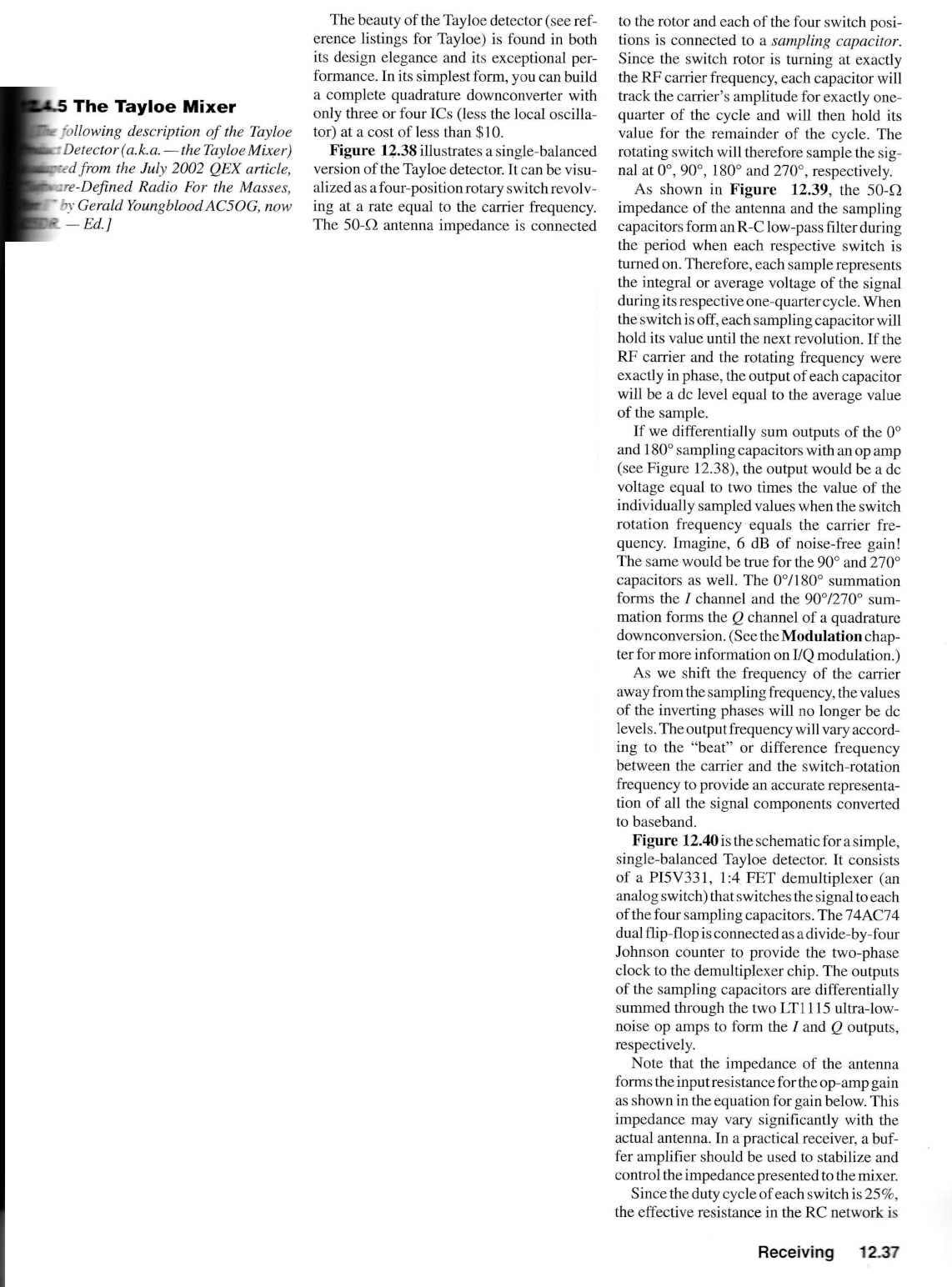
detector is for you, build its design elegance and its exceptional performance. In its simplest form, you can build a complete quadrature downconverter with only three or four ICs (the local oscillator, mixer, and amplifiers). Figure 12.38 illustrates a single-balanced version of the Tayloe detector. It can be visualized as a four-phase rotation switch revolving at a rate equal to the carrier frequency. The 50-Ω impedance of the antenna and the sampling capacitors form an R-C low-pass filter during the periods when the switch is turned on. Therefore, when the switch
inverting CMOS gate or combination of gates could be used. This means left over portions of gate packages can be often used. The duty cycle will be close to 50% and will oscillate at a frequency that is given by the fol- lowing expression. AN006022-2 FIGURE 2. Three Gate Oscillator Propagation Delay vs Ambient
This pin is Data/Command control pin connecting to the MCU. When the pin is pulled HIGH, the data at D[7:0] will be interpreted as data. When the pin is pulled LOW, the data at D[7:0] will be transferred to a command 12 D/C register. In I2C mode, this pin acts as SA0 for slave address selection. When
time, clock input pulse width and maximum frequency 9, &3▯LQSXW 90 *1' WVX VX W W 9 K K , 'Q▯LQSXW 90 *1' 92+ 4Q▯RXWSXW 90 9 2/ 92+ 4Q▯RXWSXW 90 92/ DDD▯▯▯▯▯▯▯ Measurement points are given in Table 8. Fig 8. Data set-up and hold times for data input 74HC_HCT175 All
expansion to a 1-of-32 (5 to 32 lines) decoder with just four '138 ICs and one inverter. The '138 can be used as an eight output demultiplexer by using one of the active LOW enable inputs as the data input and the remaining enable inputs as strobes. Inputs include clamp diodes. This enables the use
data (nD), clock (nCP), set (nSD) and reset (nRD) inputs, and complementary nQ and nQ outputs. Data at the nD-input, that meets the set-up and hold time requirements on the LOW-to-HIGH clock transition, is stored in the flip-flop and appears at the nQ output. Schmitt-trigger action in the clock input,
number of inputs switching; (CL VCC2 o ) = sum of outputs. 11. Waveforms 9, Q$▯▯Q%▯▯Q&▯LQSXW 90 *1' W W 3+/ 3/+ 92+ 9< Q<▯RXWSXW 90 9; 9 2/ W W 7+/ 7/+ ▯▯▯DDO▯▯▯ Measurement points are given in Table 8. VOLand V OHare typical voltage output levels that occur with the output load. Fig 6. Input to
Typ Max Min Max Min Max 74HC08 pd propagation nA, nB to nY; see Fig. 6 [1] delay VCC = 2.0 V - 25 90 - 115 - 135 ns V = 4.5 V - 9 18 - 23 - 27 ns CC VCC = 5.0 V; CL= 15 pF - 7 - - - - - ns VCC = 6.0 V - 7 15 - 20 - 23 ns t transition time see Fig. 6 [2] V = 2.0 V - 19 75 - 95 - 110 ns CC VCC = 4.5 V
Bin Category Min. Max. D 8.40 15.30 IV Bin Category Min. Max. E 12.60 23.10 Red IV Categories F 18.90 37.80 C 13.10 24.00 G 30.60 61.20 D 19.70 36.10 H 49.50 97.90 E 29.60 54.20 I 80.10 158.40 F 44.90 88.80 J 129.60 253.40 G 71.90 143.80 H 116.50 227.70 Yellow IV Categories Table 8: HLMP-2550/2855/2870

 Bild
Bild
 Bild
Bild
 Bild
Bild