For information on tape and reel specifications, including part orientation and tape sizes, please refer to our Tape and Reel Packaging Specifications Brochure, BRD8011/D. *Bidirectional devices will not be available in this se- ries. **The “T3” suffix refers to a 13 inch reel. Individual devices are
Also: Es handelt sich um einen LG Industrial Systems (LSIS.biz) Korea Serie iG5A 0,4 kW – 7,5 kW (200/400V) Installations-, Betriebs- und Wartungsanleitung LG Industrial Systems LG Variable Frequency Drives Type SV004iG5A Input 200-240V 1Ph 3.9A Output 0 - {input voltage} 2.5A 0.95kVA Bei Kleinanzeigen
Es handelt sich um einen LG Industrial Systems (LSIS.biz) Korea > Serie iG5A > 0,4 kW – 7,5 kW (200/400V) > Installations-, Betriebs- und Wartungsanleitung > LG Industrial Systems > LG Variable Frequency Drives > Type SV004iG5A > Input 200-240V 1Ph 3.9A > Output 0 - {input voltage} 2.5A 0.95kVA
nicht. Hilfe brachte https://www.eevblog.com/forum/repair/hp-3478a-how-to-readwrite-cal-sram/200/ Dort wurde der SRAM-Inhalt diskutiert und strukturiert aufbereitet und es wurden Tools zum Auslesen (und Beschreiben) entwickelt und vorgestellt. Ich habe mir vor einiger Zeit ein Keysight 82357B
Volt könnte man z.B. auch mit 3 gestapelten ("stacked") 10V-Referenzen (siehe Beispiel im Datenblatt Ref102) erzielen, aber 1% Overrange des 3478A wollen auch beachtet werden. Zum Verständnis des folgenden Textes bitte das Datenblatt der LM399, Seite 6 "Portable Calibrator" angucken. Wenn ich ein
High Power LED https://www.amazon.de/dp/B0DPH37X51/?coliid=I1HTQBV898XGQD&colid=3CG1KKTN0OJVM&ref_=list_c_wl_lv_ov_lig_dp_it&th=1 Mfg Marcel
Leitwert von weniger als 50K/250W = 0,2K/W. Weil für eine passive Kühlung dann ein Alu-KK mit mindestens 200x200mm benötigt wird, ergibt sich, dass du unbedingt auch einen Lüfter brauchst. Das passende Stichwort dazu lautet "Hohlrippe": - https://www.eureca.de/847-0-Kuehlkoerper-zur-Lieferung-in-kleinen-Stueckzahlen.html
CCDisable Threshold 7.0 8.0 8.5 V V L Logic 0 Input Voltage 1.0 1.6 – V Voltage Regulator Section V REF Output Voltage 6.25 7.00 7.50 V IO Output Load Current - - 10 mA V REF-LOAD Output Load Regulation 0 to 10 mA – 4 50 mV VREF-LINE Output Line Regulation 8.5 V ≤ VCC ≤ 16 V – 30 150 mV PRS Power Supply
is still in effect. [19:0] Reserved RO Reserved 0 For the operation or setting of FlashROM, please refer to related subprograms. This datasheet does not provide the introductions to FlashROM word data registers and FlashROM control registers. 4.4 Flash-ROM Operation Steps 1. Erase Flash-ROM, please refer to and call related subprograms. 2. Write Flash-ROM, please refer to and call the related subprograms. 3. Read DataFlash, please refer to and call related subroutines. 4. Read CodeFlash, through a pointer to the program storage space. 4.5 Unique ID Each chip has
mA 16 17 17.9 V Z CC Supply current Before device turn-ON Istart-up Start-up current V = V - 0.2 V 200 250 µA CC CC(ON) I Device ON, V = 1 V q Quiescent current STBY 1.5 2 mA op Operating current Device ON, 3.5 5 mA V STBY= V RFmin V DIS> 1.85 V or DELAY I q Residual consumption > 3.5 V or LINE< 1.25
Capability Pin10= 10 V) − 800 − mA Regulation Block V Voltage Reference NCP1605/A 2.425 2.500 2.575 V REF NCP1605B 2.430 2.500 2.550 EA Error Amplifier Current Capability − ±20 − mA G EA Error Amplifier Gain 100 200 300 mS IPin4 Pin 4 Bias Current @Pin4 VREF −500 − 500 nA VCONTROL Pin 2 Voltage: V − V MAX
off state; V< 0.8 V - 2 10 A P EN Iq quiescent current no load, snubbers and output filter - 185 200 mA connected Quad BTL channel; V P = 14.4 V P o output power RL= 4 ; THD = 10 % 24 26 - W R = 2 ; THD = 10 % 39 45 - W L Quad BTL channel; V P = 24 V P o output power RL= 4 ; THD = 10 % - 70 - W
REVISED MAY 2012 TYPICAL CHARACTERISTICS (continued) INRUSH CURRENT vs LOAD CAPACITANCE 300 250 A m 200 t VI= 5 V n r u 150 C s VI= 3.3 V r I I 100 I 50 0 0 20 40 60 80 100 CL- Load Capacitance - mF VI TPS2113A 0.1 mF f = 28 Hz 1 8 90% Duty Cycle NC STAT IN1 To Oscilloscope 2 7 EN OUT 3 6 VSNS IN2 50
Hysteresis -40°C to 125°C 2.5 3.5 4.5 % ON-RESISTANCE (INx to OUT) 25°C 62 75 mΩ OUT = -200 mA -40°C to 85°C 90 mΩ ON-State Resistance (TPS2120) V > V PRI REF -40°C to 105°C 100 mΩ VINx≥ 5.0 V -40°C to 125°C 120 mΩ R ON 25°C 56 70 mΩ I = -200 mA OUT -40°C to 85°C 85 mΩ ON-State Resistance
part has multiple moisture sensitivity ratings, only the lowest level per JEDEC standards is shown. Refer to the shipping label for the actual reflow temperature that will be used to mount the part to the printed circuit board. (6) Part marking: There may be an additional marking, which relates to the
exposure limit is exceeded and/or in case of product release (dust). Do not breathe vapours, aerosols. Refer to protective measures listed in sections 7 and 8. 6.2 Environmental precautions Environmental precautions : Try to prevent the material from entering drains or water courses. Local authorities should
the retransmission timeout period. The unit of timeout period is 100us and the default of @ref _RTR_ is x07D0. * And so the default timeout period is 200ms(100us X 2000). During the time configured by @ref _RTR_, W5500 waits for the peer response * to the packet that is transmitted by \ref Sn_CR
an der Bildlaufleiste (ohne Hovern) wie groß das Dokument ist und wo ich etwa stehe. (z.B. STM32H7-RefMan). Harald K. schrieb im Beitrag #7882013: > Fährst Du die etwa mit der Maus an, um dann den Gnubbel herumzuschieben? Meist nicht, sondern per Mausrad oder PgUp/PgDn-Taste. Ist aber egal. Harald
nicht einfach abnicken sollte: https://filestore.community.support.microsoft.com/api/images/2acfe200-c0b1-4d12-80dc-fd5e50623358?upload=true Alexander schrieb im Beitrag #7885164: > Wenn Du dich als Windows 10 oder 11 Nutzer outest, klicke mal bitte in > das Suchfeld in der Taskleiste Das Suchfeld
Dann geht es genauso, wie beschrieben. Den ADC auf maximal 200 kHz konfigurieren (so kenne ich es von den AVR), ADC-Interrupt aktivieren, Kanal auswählen und Wandlung starten. Am Ende der Wandlung das Ergebnis auslesen, den nächsten Kanal auswählen und die nächste
Florian schrieb im Beitrag #7880615: > Dann geht es genauso, wie beschrieben. > Den ADC auf maximal 200 kHz konfigurieren (so kenne ich es von den AVR), > ADC-Interrupt aktivieren, Kanal auswählen und Wandlung starten. > Am Ende der Wandlung das Ergebnis auslesen, den nächsten Kanal auswählen > und
may result in discomfort or serious injury. Refer to the Safety & Comfort Guide at http://www.hp.com/ergo for more information on choosing a workspace and creating a safe and comfortable work environment. For more information, refer to the Safety
receive interrupt notification when V DD drops to the PVD threshold or rises to the PVD threshold. Refer to Chapter 4 for the values oPOR/PDRand V PVD . 1.4.5 Voltage regulator After reset, the regulator is automatically turned on, and there are 3 operation modes according to the application mode. ON
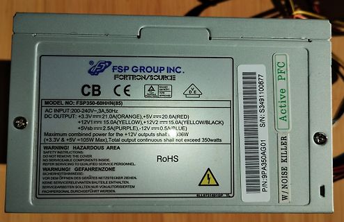
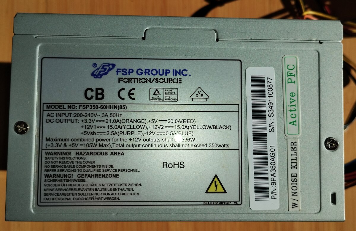
FSP GROUP INC.
FORTRON/SOURCE
CB CE
MODEL NO: FSP350-60HHN(85)
AC INPUT: 200-240V~, 3A, 50Hz
DC OUTPUT: +3.3V==21.0A(ORANGE), +5V==20.0A(RED)
+12V1==15.0A(YELLOW), +12V2==15.0A(YELLOW/BLACK)
-12V==0.5A(BLUE)
Maximum combined power for the +12V outputs shall be 336W
(+3.3V &
Die Ausgangsstufe des INA entspricht funktionell Deinem > OP2A. > Wenn Du direkt die Spannung am REF-Eingang des INA manipulierst, > kannst Du im Prinzip einen der nachgeschalteten OPVs sparen. Jetzt verstehe ich es. Aber braucht man dafür nicht eine negative Spannung an Ref, wenn man den Offset
Florian schrieb im Beitrag #7878337: > Aber braucht man dafür nicht eine negative > Spannung an Ref, wenn man den Offset abziehen will? Nein; der Ausgang ist Ref + (Sig+ − Sig−) × Verstärkung. Ein auf beiden Eingängen vorhandener Offset fällt automatisch weg.
1985, half-duplex. 5.2 Transmission speed Initial baud rate – 300 Standard baud rates – 300, 600, 1 200, 2 400, 4 800, 9 600, 19 200 Special baud rate – as desired. NOTE The maximum speed may be limited by the reading head or the optical port or the ITU-T Recommendation V.28 limitations in the tariff
immer eine Last anliegt, damit das Akkupack konstant Strom liefert. Habe es mit einem 100 Ohm und 200 Ohm Widerstand probiert. Allerdings hatte das kein Erfolg. Die Datenleitungen hatte ich dabei verbunden. Vielleicht kann ja wer helfen, ich wollte nicht den Akku im Rekorder ersetzen. Danke
doch reichen... https://www.amazon.de/-/en/Switch-Intelligent-Module-Remote-Control/dp/B0D456KS99/ref=sr_1_4?crid=3UGP4EIVOV34E&dib=eyJ2IjoiMSJ9.XVDlTSrptf4wWQM8LfhDaRtoNWkRv-Yi1Y2sLshX5b8djUjylAaPL6j0W08C7lwzN9KWbCT_QViQcY9FnWF97jG-pu37zhiP9m1E13V_5_o-XKOomAQv578KMh3nbJQNH6f3cPOjLZuBYudrttzKMKZd3OXgKb2KF6OCxt_bIoJcoSKnmyjKlLP
3455,07 EUR Die dreistellige Zahl am Ende des Links entscheidet also darüber, ob das Notebook bis zu 200 EUR billiger oder 500 EUR teurer wird. P.S. Den Parameter utm_source=geizhals kann man sogar weglassen, es reicht ?ref=103, um den günstigeren Preis zu bekommen. Sollte man immer den teuersten
Nee, der Preis wurde wohl zwischenzeitlich gesenkt. Ich bekomme die 3085,86 € mittlerweile auch für ref=103 :-) Übrigens: Idealo nutzt ref=109. Jacob scheint da aber nicht mehr gut drauf zu sprechen sein, denn dann kommt immer der teuerste Preis. Welche Preissuchmaschine ref=125 bzw ref=126 nutzt,
these registers, the value of single bits can be checked by using the SBIS and SBIC instructions. Refer to the instruction set section for more details. When using the I/O specific commands IN and OUT, the I/O addresses $00 - $3F must be used. When addressing I/O Registers as SRAM, $20 must be added
etwas googlen hilft da evt. auch weiter: https://english.electronica-pt.com/repair-tips?marca=Sony&ref=KV-M1400 https://english.electronica-pt.com/repair-tips?ref=BE2&marca=&sintoma=&page=1c
Schaltkreis Problem > - G2 Poti korrodiert Stromversorgung .... Bildrohrplatine - messen (190-200V ca.) Generelle Stromversorgung - messen Blanking Schaltkreis Problem - NEIN G2 Poti korrodiert - NEIN - verdrehen - schon tausendmal gebettelt. Es ist völlig piepewas du mit einem Voltmeter an
Supply Pin. Must be locally bypassed. Functional Block Diagram FB SW 3 1 SOFT START OV 5 OV DRIVER V 200mV A1 VIN 6 REF A2 CONTROL Q1 1.25 V LOGIC OVER COMPARATOR TEMPERATURE DETECTOR 2 GND CTRL 4 STANDBY RAMP To Control GENERATOR Logic 1MHz OSCILLATOR Absolute Maximum Ratings (Note 5) Symbol Parameter
seit 35 Jahren auf mehr oder weniger gebrauchen Computer .. VC20, C64, Amiga, Jede Menge PCs: Cyrix 200+, Pentium 300, 566, 1300 usw von den Thinkpads gar nicht zu reden. Danke + MfG Wolfgang
mit 12V: https://www.amazon.de/Universal-Netzteil-Ladekabel-Pavilion-Adapterstecker/dp/B0CF54WKQJ/ref=sr_1_4
0.08V 3.00±0.1V 300±30mV -210±30mV available A HY2120-BB 4.35±0.025V 4.15±0.05V 2.30±0.08V 3.00±0.1V 200±30mV -210±30mV available A HY2120-CB 4.28±0.025V 4.08±0.05V 2.90±0.08V 3.00±0.1V 200±30mV -210±30mV available A . HY2120-DB 4.28±0.025V 4.08±0.05V 2.25±0.08V 2.95±0.1V 200±30mV -210±30mV available A
der Feldstärkepegel (in dBμV/m) der jeweiligen Konfiguration zur Referenzmessung gebildet. A E (LE,Ref LE,Konf) dB (4) j Die Ergebnisse sind in den Bildern 11 und 12, getrennt nach horizontaler und vertikaler Polarisation, dargestellt. Bild 10: Maximaler Feldstärkepegel in 10 m Entfernung (Referenz ohne
www.amazon.de/AILOOCEDI-BNC-Buchse-Adapter-BNC-Buchse-50KY-Q9-Adapter-Anschlusszubeh%C3%B6r/dp/B0D1GH9WMB/ref=sr_1_3? und baut einen Messwiderstand nach eigener Vorstellung ein.
Erdmagnetfeldes mehr sieht als seine "Stromspitze" auch nicht weiter helfen. Der OP schreibt was von 2..200mA. 200mA lassen sich selbst mit den billigen Zangen schon sehr gut einordnen. 2mA sind unwichtiges Rauschen. Wenn er sich dann noch die Bandbreite der Zange und seines Oszis anschaut, kommt er auch
provided they receive additional support such * as anchoring to the PC board with epoxy resin. * Refer to 5. Conditions for operation, transport and storage mentioned in * AMBIENT ENVIRONMENT (Page 49) TYPICAL APPLICATIONS Telecommunications equipment, alarm textile machinery, elevators, control business
) Value might change after device evaluation has finished. Notes 1. n: Number of macro instances. Refer to the User Manual for the detailed specification. 2. m: Number of channels. Refer to the User Manual for the detailed specification. Notes 1. n: Number of macro instances. Refer to the User Manual
VREG Enabled 1 Supply Current Suspended; — 120 220 μA VREG Enabled 2 Supply Current—USB Pull-up — 200 228 μA Specified Operating Temperature Range –40 — +85 °C Notes: 1. If the device is connected to the USB bus, the USB pull-up current should be added to the supply current to calculate total required
Zum Thema TS101, dazu habe ich zwei gefunden. - MINIWARE Smart Soldering Iron TS101 - TS101PTS200 Ich nehme an, der empfohlene Lötkolben ist der Miniware? Wobei den gibt es in unterschiedlichen Ausführungen. TS101-BC2/-B2/-I???
besseren C245 https://www.amazon.de/YIHUA-982-III-Pr%C3%A4zise-L%C3%B6tstation-Kit-C245/dp/B0CMLQRDMS/ref=asc_df_B0CMLQRDMS Ja, es gibt auch welche mit Akku oder USB C, die sind aber trotz gleicher Lötspitze nicht so leistungsfähig. So eine Yihua982 erfüllt NICHT kompakt kabellos brandmalerei
R0 R2o3sR2BC \ı R2 9 e n R2 IEIEEI QBBK M 5 20 llCR20 A 5 S R2O7R2 REZOOTB 05% E NÜN fillRl ı\ O u 200V m X =< T: BFRT93 T2003 T4 C2157 C C C C TLOBZ R2u75 c b C200T 5 oc M; N5'“ c2oTT BFT92 Q LÜC2002 t e O Tb OKO%. 9; :zum 2 ct ° c2oı2 W015 0.1uF 2 OK2 UK UK 0 fK +T2\/ t JZOOI 200V R20Ü5 RO84IR085 RZOBESR2E7
restricted Page 1 of 3 Product / Process Change Notification N° 2020-176-A Products affected: Please refer to attached affected product list 1_cip20176_a Detailed Change Information: Subject: Capacity extension with introduction of an additional assembly and final test location at Huayi Microelectronics
Junction-ambient max. 85 13 (*) 60 35 (*) Mounted on aluminium substrate. ELECTRICAL CHARACTERISTICS (Refer to the Test Circuits; T = 25⋅C, V = j2V, V S sens= 0, unless otherwise specified). Symbol Parameter Test Conditions Min. Typ. Max. Unit V s Supply Voltage 12 36 48 V Vref Reference Voltage REF = 2mA
VREG Enabled 1 Supply Current Suspended; — 120 220 μA VREG Enabled 2 Supply Current—USB Pull-up — 200 228 μA Specified Operating Temperature Range –40 — +85 °C Notes: 1. If the device is connected to the USB bus, the USB pull-up current should be added to the supply current to calculate total required
wiki/EIA-485) und TI-Datenblatt (https://www.ti.com/lit/ds/symlink/sn65hvd3082e.pdf?ts=1743498914859&ref_url=https%253A%252F%252Fwww.mouser.at%252F) richtig verstehe, ist A (auch + genannt, "nichtinvertierend") im Ruhezustand High B (auch - genannt, "invertierend") im Ruhezustand Low Ruhezustand heißt
der Steuerung einen Spannungsteiler. Das ist nicht weiter schlimm, solange die Differenz mindestens 200mV beträgt, aber wenn der Hersteller auch keine Terminierung verbaut hat, lass sie einfach weg.
www.amazon.de/WITTKOWARE-PT-65C-Frame-Netzteil-Ausg%C3%A4nge/dp/B08KS95R91?source=ps-sl-shoppingads-lpcontext&ref_=fplfs&smid=A2PNNIYOUQZRLT&th=1 Man findet genug wenn man sucht. Gruß D.T.
www.amazon.de/WITTKOWARE-PT-65C-Frame-Netzteil-Ausg%C3%A4nge/dp/B08KS95R91?source=ps-sl-shoppingads-lpcontext&ref_=fplfs&smid=A2PNNIYOUQZRLT&th=1 > > Man findet genug wenn man sucht. > > Gruß > D.T. Wer lesen kann ist immer am Vorteil! Ich habe maximae Dimensionen schon zweimal bisher erwähnt
Hole External Shaft Shaft Length (with tachometer)iameter Length Spacing Dimension Diameter Length (Ref) (Ref) (Ref) (Ref) (Ref) DPP240 4.0 in 6.1 in 0.2500 in 0.2495 in [4] 6-32 UNC-2B DPP242 5.0 in 7.1 in 1.00 in 1.000 in 0.10 in 0.38 in Deep Min 1.083 in 2.00 in 0.2497 in 0.70 in 0.74 in ±0.03 0.998

 Bild
Bild
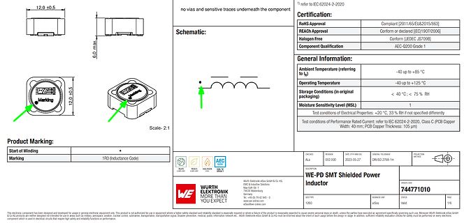
 Bild
Bild