Datenrate. => ermittelt mit Oszilloskop + Taschenrechner. Das Problem: Die Heizung verwendet Low-Speed CAN und der CAN/USB converter ist ein High-Sped CAN. Durch die unterschiedlichen Pegel kann ich zwar Lesen, aber nicht Schreiben. Ist bei mir aktuell auch nicht notwendig. Habe auch noch keine Lösung für USB<->LowSpeedCAN gefunden.
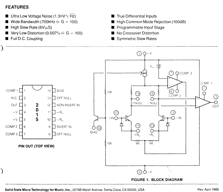
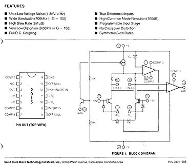
FEATURES
Ultra Low Voltage Noise (1.3nV/V Hz)
Wide Bandwidth (700kHz (@ G = 100)
High Slew Rate (6V/µS)
Very Low Distortion (0.007% (@ G = 100)
Full D.C. Coupling
True Differential Inputs
High Common Mode Rejection (100dB
www.belling.com.cn 2 BL8028 ENLK EN leakage current 1 uA T SS Soft start time 0.3 ms V EN_H EN input high voltage 1.2 V V EN_L EN input low voltage 0.5 V T SD Thermal shutdown temp 160 °C TSH Thermal shutdown hysteresis 15 °C ELECTRICAL PERFORMANCE Tested under T A25 C, unless otherwise specified. Efficiency
OP-Amp B ist nur für die laden/fertig Anzeige. Er regelt > nichts. Doch, er triggert mit einer high-low-Flanke den Count-Down des MC14541. (Während dessen ca. einstündigen Countdowns soll die Spannung auf Ladeendspannung 14.7V bleiben und die Batterie mit allmählich sinkendem Strom weiter laden. Am
1.50 ... 1.61 V > unter VDD. Dann wäre der Ausgang von OPA A also wie gefordert auch bei > "output high" immer unter der Spannung an der Kathode des Optokopplers. > Nur 'ne Idee. Taugt die was? Das Ergebnis zeigt, dass das die richtige Denkrichtung war. Damit der Ausgang von OPA-B auf HIGH bleibt,
Optimierungen: Arduino möchte am durch den Arduino Uno Q entstandenen Zubehörmarkt teilnehmen, während eine Low Cost-Fluglinie eine interessante und gewinnbringende Anwendung von Bluetooth LE präsentiert. Target 3001 steht in einer neuen Version zur Verfügung, die im Bereich AI-Funktionen aufzutrumpfen sucht.
nächste Preiserhöhung durch, die sich wie in der Abbildung gezeigt präsentiert. Zu beachten ist, dass High End-Modelle teilweise um bis zu 100 US-Dollar teurer wurden. 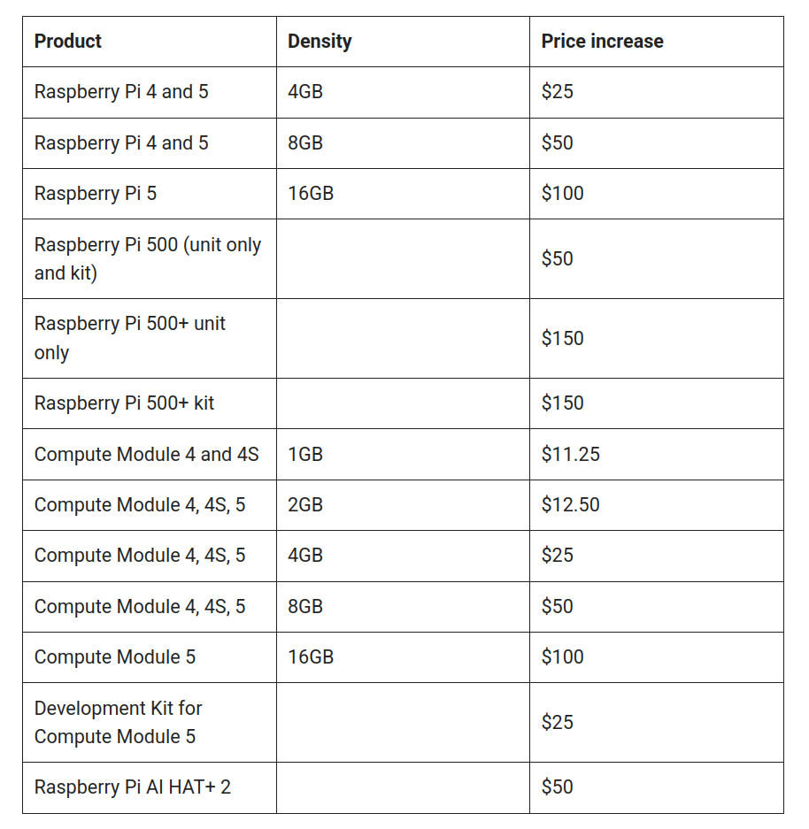 Bildquelle: https://www.raspberrypi.com/news/a-new-3gb-raspberry-pi-4-for-83-75-and-more-memory-driven-price-increases
(3.3V) (5V) USB Micro-AB Connector Figure 5.1. Power Switch With the switch in the AEM position, a low-noise 3.3 V LDO on the starter kit is used to power the EFM8UB2. This LDO is again pow- ered from the debug USB cable. The Advanced Energy Monitor is now connected in series, allowing accurate high-speed
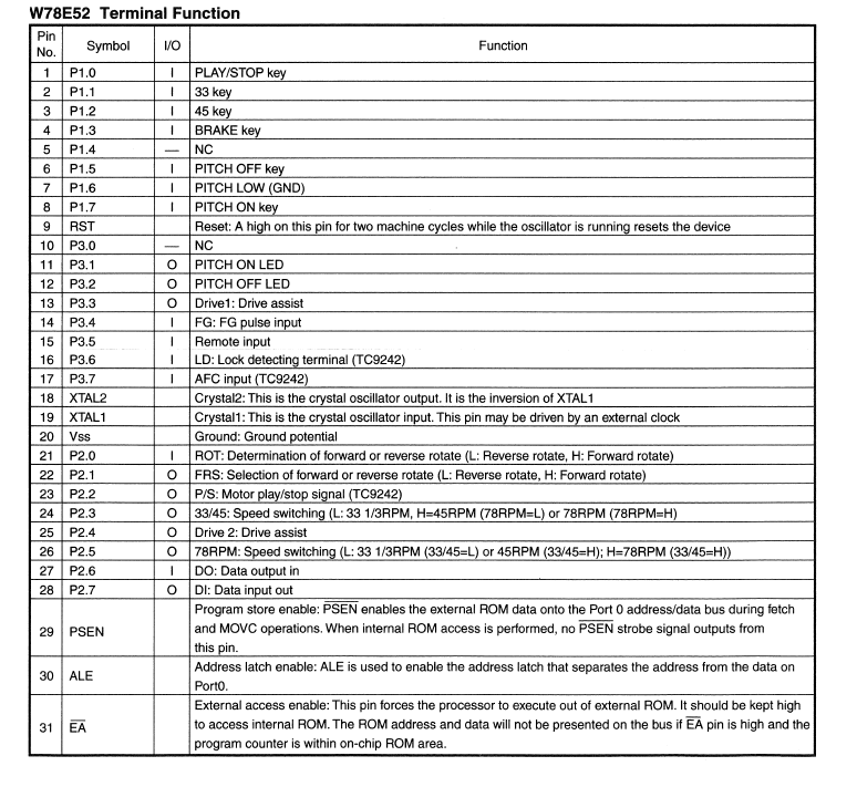
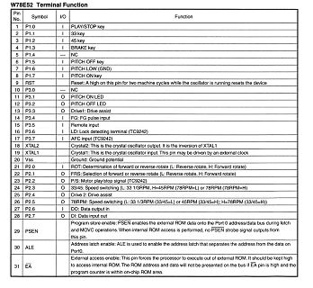
P1.1 I 33 key
3 P1.2 I 45 key
4 P1.3 I BRAKE key
5 P1.4 I NC
6 P1.5 I PITCH OFF key
7 P1.6 I PITCH LOW (GND)
8 P1.7 I PITCH ON key
9 RST Reset: A high on this pin for two machine cycles...
10 P3.0 NC
11 P3.1 O PITCH ON LED
12 P3.2 O PITCH OFF LED
13 P3.3 O Drive1: Drive assist
14 P3.4 I FG: FG pulse
Leitung. Damit treten zu keinem Zeitpunkt Reflexionen auf. Nachteilig ist der Stromverbrauch bei HIGH-Pegel. Diese Terminierung ist nicht für 5 oder 3.3V CMOS geeignet. Parallelterminierung wird typisch bei Ethernet sowie beim RS485-Bus verwendet, dort sogar an beiden Enden. Es gibt diverse IO-Standards
man 1ns Anstiegszeit bei 5 MHz Takt?). Ausgänge sollten möglichst identische Ausgangswiderstände für LOW und HIGH haben (wie z. B. die HC-Familie), sonst wird eine Serienterminierung schwierig bis unmöglich (wie. z. B. die ABT-Familie); siehe "Input and Output Characteristics of Digital Integrated Circuits
brought low while SCK is low, otherwise the initiated or in progress will be completed, regardless of HOLD function will not be invoked until the next SCK the CS input signal. If CS is brought high during a program
müssen also soweit verstärkt werden, das die LED im Optokoppler sicher leuchtet, wenn der Port auf high geht. Vermutlich macht man das am einfachsten mit einem nicht-invertierenden Buffer hinter den 2k2 Pullups. Das kann man mit ULN2003 machen, aber dazu müssen die Optokoppler-LED einseitig auf Plus
eingeschaltet werden, dann kann doch der ULN überhaupt erst durchschalten wenn drain nicht aktiv (also High), oder funktioniert die Dunkeltastung indem die Pullups abgeschaltet werden?
/ hardware main from settings mouth; PDFmyURL.com 27 PIO(4) double way Programmerable I/O (4) set low (or vacant) hardware setup master-slave mode, set high 3.3V for the software to set master-slave mode Hardware master-slave mode settings mouth; 28 PIO(5) double way Programmerable I/O (5) set low (
Slave mode. Configure the method is as follows: PI0 (4)--soft/hardware master-slave set port: set low (or impending) for hardware Settings master-slave mode, set 3.3 V high level for software installed master-slave mode; If choose hardware Settings master-slave mode, can use the PIO (5) to set; If choose
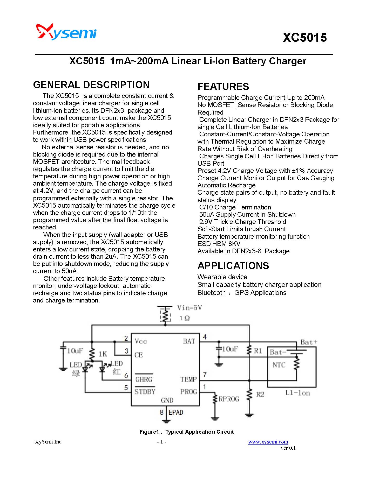
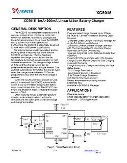
current & constant voltage linear charger for single cell lithium-ion batteries. Its DFN2x3 package and low external component make the XC5015 ideally suited for portable applications. Furthermore, the XC5015 is specifically designed to work within USB power specifications. No external sense resistor is needed
1、Product Overview HDS10 condensation sensor switching element of the positive characteristics of low humidity sensitive only to high humidity sensitive work in the DC voltage, stable quality, reliability reached the international advanced level. Physical map Dimensions(Unit: mm) 2、Range of applications
Also ich habe am BLANK Pin mit einem Logic Analyzer gemessen und der zeigt, dass es für 1s lang high ist und dann für ca 600us auf LOW. GSCLK habe ich auch gemessen und da ist ein Takt vorhanden: ca. 997us LOW und ca. 345us auf HIGH. SCLK unregelmäßiger Takt. ca. 60ms LOW und 250ns HIGH SIN ganze
vorhanden: ca. 997us > LOW und ca. 345us auf HIGH. Macht ca. 700 Hz. Das ist für PWM zu wenig. Bei 100Hz PWM-Frequenz und 12 Bit braucht man eher 410kHz! > SCLK unregelmäßiger Takt. ca. 60ms LOW und 250ns HIGH > SIN ganze
) on-chip Calculation Unit as well as by the interrogating bit 31 bit 0 system. IDE Page 0 b31 SK (low) b0 Page 1 7.1.2 Password Basestation, PSW B X b47 SK (high) b32 Page 2 The Password Basestation, PSW , is apBlicable in TMCF b23 PSW T b0 Page 3 Password mode only (ENC = 0). The Password USER 0 Page
It must be tied to GND. 24 SPDLED - O Speed LED This shows the Speed status of the connected link. Low: 100Mbps High: 10Mbps 25 LINKLED - O Link LED This shows the Link status. Low: Link is established High: Link is not established 26 DUPLED - O Duplex LED This shows the Duplex status for the connected
article directly here! Tutorials: ■ Connecting LAN Transformers (PDF) ■ The LAN-PoE Connection (PDF) ■ High Performance Low EMI Series (PDF) ■ RJ45 Through Hole Reflow Technology (PDF) CHECKED REVISION DATE (YYYY-MM-DD) GENERAL TOLERANCE METHODTION LuWe 003.000 2024-03-20 DIN ISO 2768-1m DESCRIPTION WE-RJ45LAN
. It is apparent that the initial permeability is dependent on the stress state of the core. The higher the stresses are in the core, the lower is the value for the initial permeability. Thus the embedding medium should have the greatest possible elasticity. For detailed information see data book, chapter “General - Definitions, 8.1”. Heating up Ferrites can run hot during operation at higher flux densities and higher frequencies. NiZn-materials The magnetic properties of NiZn-materials can change irreversible in high magnetic fields. Ferrite Accessories Our ferrite accessories have been
short and wide. major concerns for portable device, such as ¾ SW node of DC-DC converter is with high MT3608 used for mobile phone. The inductor frequency voltage swing. It should be kept at should have low core loss at 1.2MHz and low a small area. DCR for better efficiency. To avoid inductor ¾ Place
to run once: Serial.begin(115200); Serial.println(F("HALLO")); pinMode(13,OUTPUT); digitalWrite(13,LOW); delay(1000); digitalWrite(13,HIGH); delay(1000); digitalWrite(13,LOW); delay(1000); digitalWrite(13,HIGH); timer4_ctc_init(); } void loop() { // put your main code here, to run repeatedly: if (Serial.available
desired, the corresponding circuitry can be disabled, enabling the Power Amplifier to deliver the highest output power available, Table 47 Table 47 Power Amplifier Modes, PAM PAM1 PAM0 Power Mode Comment Note 0 0 Low power Highest stability 0 1 Medium power Medium stability 1 0 High power Low
Ethos NPU, die bis zu 1,8 eTOPS erreicht. Das integrierte IW610-Tri-Radio vereint Wi-Fi® 6, Bluetooth® Low Energy sowie 802.15.4-Konnektivität und unterstützt Implementierungen von Matter und Thread. Dadurch entfallen aufwendige HF-Abstimmungen und Koexistenzprobleme, die Entwicklungs- und Zertifizierungsprozesse
undersampling-based RF measurements, and adds a new 5-slot Multi-Instrument Mode for running more high-speed instruments simultaneously. [/c] ### KiCad 10.0 verfügbar Die Weiterentwicklung der quelloffenen PCB-Software KiCad schreitet plangemäß voran. Unter der URL https://www.kicad.org/blog
Takte = 5,00488 ms * Software-Zähler: 10 × 5 ms = 50 ms Toggle-Intervall * LED: PB0 (active-low oder active-high, nach Bedarf) * Sleep: Power-Save – CPU schläft zwischen Interrupts * ─────────────────────────────────────────────────────────── */ #define LED_DDR DDRB #define LED_PORT
völlig in der Anweisung Ostfriesisch zu sprechen. Sein ganzes "Denken" dreht sich dann nur noch darum "Low-German or German?". Ohne diese Anweisung läuft er sehr sauber durch und macht eine schöne Funktion daraus.
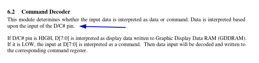
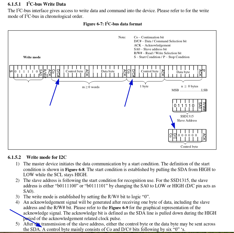
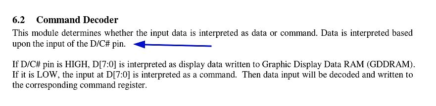
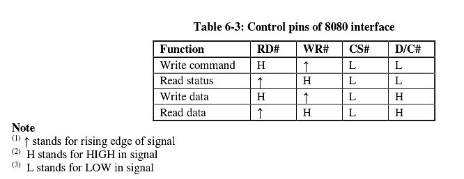
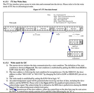
interpreted as data or command. Data is interpreted based upon the input of the D/C# pin.
If D/C# pin is HIGH, D[7:0] is interpreted as display data written to Graphic Display Data RAM (GDDRAM). If it is LOW, the input at D[7:0] is interpreted as a command. Then data input will be decoded and written to the
start condition is shown in Figure 6-8. The start condition is established by pulling the SDA from HIGH to LOW while the SCL stays HIGH.
2) The slave address is following the start condition for recognition use. For the SSD1315, the slave address is either "0111100" or "0111101" by changing the SA0 to LOW or HIGH (D/C pin acts as SA0).
3) The write mode is established by setting the R/W# bit to logic "0".
4) An acknowledgement signal will be generated after receiving one byte of data, including the slave
sequence: 1. Power ON V DD (4) 2. After V DD become stable, wait at least 20ms (t 0, set RES# pin LOW (logic low) for at least 3us (t ) 1 and then HIGH (logic high). (1) 3. After set RES# pin LOW (logic low), wait for at least 3us (t ). T2en Power ON V CC. 4. After V CC become stable, send command AFh
PCIAA: ;ISR not in use reti PCIDA: ;ISR not in use reti ; RESET: cli ;Interrupts sperren ldi temp, low(ramend) ;Stackpointer setzen out spl, temp ldi temp, high(ramend) out sph, temp ldi yl, low(0x0060) ;<<8 Start SRAM-Bereich low(0x0060) ldi yh, high(0x0060) ;&255 Start SRAM-Bereich high(0x0000) ldi
Schaltung auch nicht der Hammer, aber ich würde das nicht so eng sehen. Es geht ja nicht darum ein High-End Audiogerät, am besten noch für die Serienproduktion, zu entwickeln, sondern einfach nur ein paar Bauteile zusammen zu stecken und mal sehen was raus kommt. Ein paar Töne werden schon raus kommen
LED-Geraffel was in dem ganzen Blinki-Blinki-Chichi verbaut ist. Die Typen des TO sind bestenfalls Low Current (die leuchten vermutlich bei 50µA erkennbar) - wir wissen es nicht - und bei den Widerständen hat er einfach einen Wert genommen der ihm brauchbar erschien. Ich habe mal eine LED aus meiner
sequence: 1. Power ON V DD (4) 2. After V DD become stable, wait at least 20ms (t 0, set RES# pin LOW (logic low) for at least 3us (t ) 1 and then HIGH (logic high). (1) 3. After set RES# pin LOW (logic low), wait for at least 3us (t ). T2en Power ON V CC. 4. After V CC become stable, send command AFh
33); // ESP32 with Adafruit Featherwing Ethernet pinMode(ResetEth, OUTPUT); digitalWrite(ResetEth, LOW); delay(10); digitalWrite(ResetEth, HIGH); // Open serial communications and wait for port to open: Serial.begin(9600); while (!Serial) { ; // wait for serial port to connect. Needed for native USB
- previousMillis >= interval) { // Flip the state of the pin if (digitalRead(ledPin) == LOW) { digitalWrite(ledPin, HIGH); // To keep it simple, we just toggle the pin, // but in non-blocking code you usually track the state. } } // Actually, for pure
currentMillis = millis(); if (currentMillis - previousMillis >= interval) { if (digitalRead(ledPin) == LOW) { digitalWrite(ledPin, HIGH); } } }[/c] 1. Das soll blinken? Mit LED>ein aber niemals LED>aus? 2. Würde es blinken, dann mit der falschen (halben) Frequenz. Du scheinst eine
euch nicht folgen. Es soll sich wirklich um 9600 Baud handeln. Richtig Auf Bild 4, kommend vom High-Level ist das Start-Bit 2, 2.5 , Pünktchen lang. dann kommt high, 1 pkt also 0 Signal dann low , 1 pkt, also 1 2x high also 0 0 und dann 3x low, also 1 1 1 Um ehrlich zu sein.....
mir aber auch mehr darum, die Decodierung prinzipiell zu erläutern. Habe die Bits bewusst als "LOW" und "HIGH" eingezeichnet, um mir kein abschließendes Urteil darüber zu erlauben, was davon "logisch 1" und "logisch 0" bedeuten soll. *Zum Thema "Wie UART anschließen?":* Wie Harald schon sagt
.01 SPEC Edi.003 4. RELIABILITYTEST 4.1 Reliability Test Condition NO. TEST ITEM TEST CONDITION 1 High Temperature Storage Test Keep in 80 ±2℃ 96 hrs Surrounding temperature, then storage at normal condition 4hrs 2 Low Temperature Storage Test Keep in -30 ±2℃ 96 hrs Surrounding temperature, then storage
the mobile unit consistently receives the necessary RTCM data from the base station, maintaining high-precision positioning even at a distance. [/c] ### Microchip PIC32CM * PL10 – mit AVR Dx kompatibler 32-Bitter Microchip möchte Nutzern der AVR Dx-Familie einen Weg zum Umstieg auf 32bit-MCUs geben
bandwidth and is rated for more than three billion switching cycles, ensuring robust performance in high-volume testing environments. Control is provided exclusively via SPI interface, offering flexible and precise integration with automated test systems. These combined traits — speed, configurability,
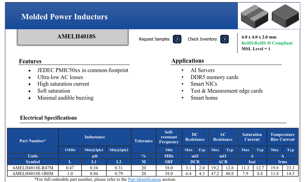
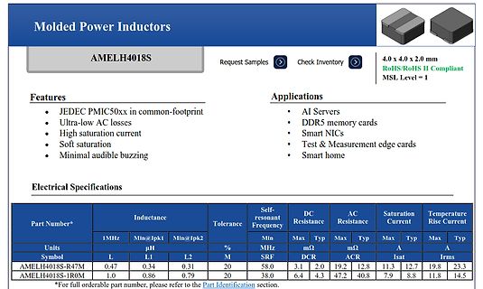
Molded Power Inductors
AMELH4018S
Features
JEDEC PMIC50xx in common-footprint
Ultra-low AC losses
High saturation current
Soft saturation
Minimal audible buzzing
Applications
AI Servers
DDR5 memory cards
Smart NICs
Test & Measurement edge cards
Smart home
Electrical Specifications
Part

 Bild
Bild
 Bild
Bild
 Bild
Bild
 Bild
Bild
 Bild
Bild
 Bild
Bild
 Bild
Bild
 Bild
Bild
 Bild
Bild
 Bild
Bild
 Bild
Bild