-
PDF
4050PBC.pdf
applications. In these applications the CD4049UBDT -55 to 125 16 Ld SOIC CD4049UB and CD4050B are pin compatible with the CD4049UBDW -55 to 125 16 Ld SOIC Buffer/ CD4009UB and CD4010B respectively, and can be Con- CD4049UBDWR -55 to 125 16 Ld SOIC
in „Pegelwandler SD-Karten tauglich“ · Mikrocontroller und Digitale Elektronik ·
-
Bild
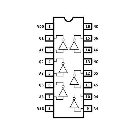
Pinbelegung eines integrierten Schaltkreises
VDD 1 16 NC Q1 2 15 Q6 A1 3 14 A6 Q2 4 13 NC A2 5 12 Q5 Q3 6 11 A5 A3 7 10 Q4 VSS 8 9 A4
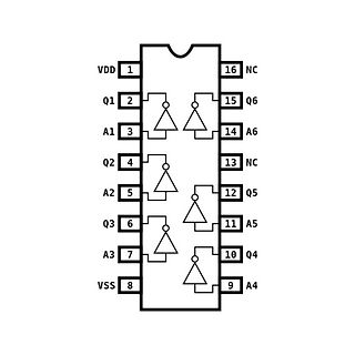
in „Brettspiel - Lautsprecher zu leise“ · Analoge Elektronik und Schaltungstechnik · · Schaltpläne
-
Datei
cd4066.txt
CGSO=93.6N CGDO=78N CGBO=128N) .ENDS .SUBCKT INVERT 1 2 3 4 * Inverter In Out Vcc Vss M1 2 1 3 3 CD4049P M2 2 1 4 4 CD4049N .MODEL CD4049P PMOS (LEVEL=1 VTO=-2.9 KP=2M GAMMA=3.97U + PHI=.75 LAMBDA=1.87M RD=28.2 RS=45.2 IS=31.2F PB=.8 MJ=.46 + CBD=21.2P CBS=25.4P CGSO=31.2N CGDO=26N CGBO=42.8N) .MODEL CD4049N NMOS (LEVEL=1 VTO=2.1 KP=5M GAMMA=3.97U + PHI=.75 LAMBDA=1.87M RD=4.2 RS=4.2 IS=31.2F PB=.8 MJ=.46 + CBD=21.2P CBS=25.4P CGSO=31.2N CGDO=26N CGBO=42.8N) .ENDS
in „CD4066 LTSpice“ · Analoge Elektronik und Schaltungstechnik ·
-
Bild
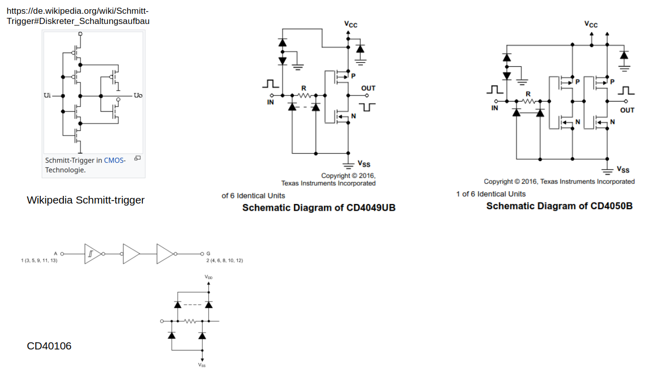
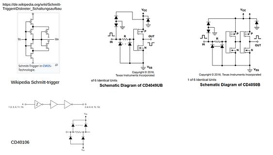
Zusammenstellung verschiedener Schaltpläne von Schmitt-Triggern
Schmitt-Trigger#Diskreter_Schaltungsaufbau Schmitt-Trigger in CMOS-Technologie. Ui Uo IN OUT Vcc Vss R N P CD4049UB CD4050B CD40106 VDD VSS
in „LtSpice CMOS simulieren 74HCxx“ · Analoge Elektronik und Schaltungstechnik · · Screenshots
-
PDF
Ca3162.pdf
5 7 8 VIN 1013 7 4 x 100kΩ GAIN +5V 10kΩ G5 16 1 +5V 6 4 TO LSD G7 G9 2 CD4056B OF LCD G1 - G6: CD4049UB 3 HEX INVERTER 5 G7, G8, G9: CD4023B 7 8 TRIPLE 3 INPUT NAND GATE TO LCD G8 BACKPLANE 15kΩ 100kΩ 0.63µF FIGURE 3. TYPICAL LCD APPLICATION 5 CA3162 CA3162E Common-Cathode, LED Display Application
-
PDF
CA3162.pdf
than displaying EEE, as with the CA3161E. segment b of the MSD is displayed. One inverter from the CD4049B is used to operate the decimal points. By connect- When displaying negative voltage, the first digit remains blank, instead of (-), and during a negative or positive over- ing the inverter input to
-
PDF
CA3162.pdf
greater than nine. After 999mV the display blanks rather MSD is displayed. One inverter from the CD4049B is used to than displaying EEE, as with the CA3161E. When displaying operate the decimal points. By connecting the inverter input to negative voltage, the first digit remains blank, instead of (-)
in „Siebensegment Multiplexing - Transistorschaltung“ · Analoge Elektronik und Schaltungstechnik ·
-
Bild
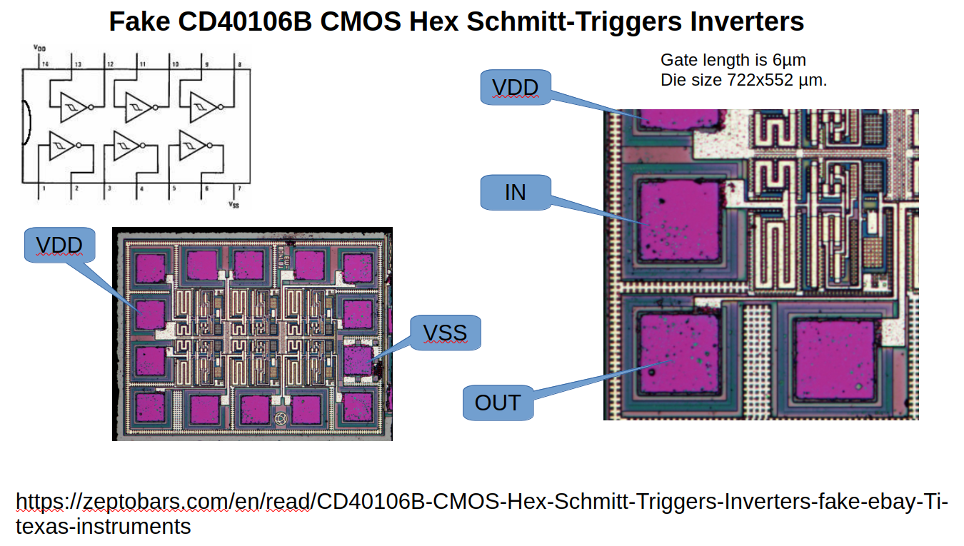
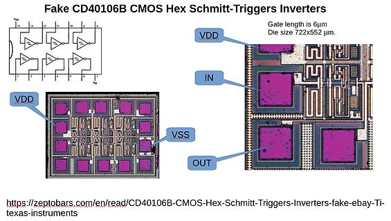
Vergleich Schaltplan und Mikroskopaufnahme eines Fake CD40106B Chips
Fake CD40106B CMOS Hex Schmitt-Triggers Inverters Gate length is 6µm Die size 722x552 µm. VDD IN OUT VSS https://zeptobars.com/en/read/CD40106B-CMOS-Hex-Schmitt-Triggers-Inverters-fake-ebay-Ti-texas-instruments
in „LtSpice CMOS simulieren 74HCxx“ · Analoge Elektronik und Schaltungstechnik · · Screenshots
-
Bild
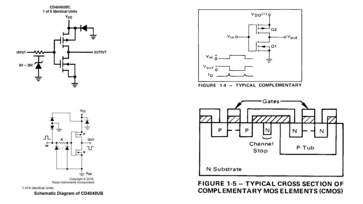
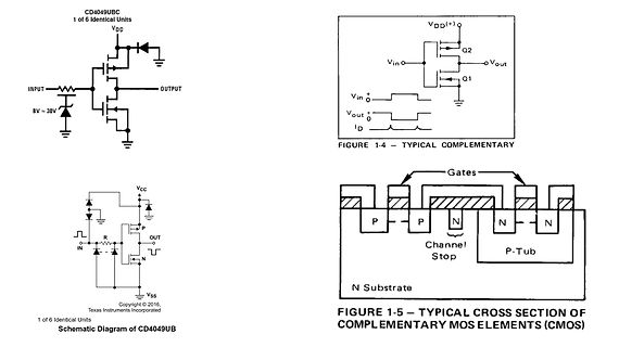
Schaltpläne und Querschnitt eines CMOS-Elements
CD4049UBC 1 of 6 Identical Units VDD INPUT 8V ~ 38V OUTPUT FIGURE 1-4 - TYPICAL COMPLEMENTARY Vin Q2 Q1 Vout Id VDD(+) Vcc P R N IN OUT Vin Vss Texas Instruments Incorporated Copyright © 2016. 1 of 6 Identical Units Schematic Diagram of CD4049UB Gates Channel Stop P-Tub N Substrate FIGURE 1-5 - TYPICAL CROSS SECTION OF COMPLEMENTARY MOS ELEMENTS (CMOS)
in „LtSpice CMOS simulieren 74HCxx“ · Analoge Elektronik und Schaltungstechnik · · Schaltpläne
-
PDF
3_5_stelliges_LED-Panelmeter.pdf
11247n 1 +SV 4148 ·R7 01 Q (4 CS (6 (7 + 11ou ~ . - 1~1 l470Kl 'Y' 1 1 1 1 1 1 l~ 4a /h 16V N1-N6=1C1=CD4049 10 Masse - Schaltbild des Low-Cost-3,Sstelligen LED- Panelmeters Sämtliche Bauelemente finden auf einer Stückliste: einzigen, übersichtlich gestalteten Leiter Low-Cost 3,Sstelliges LED-Panelmeter platte
in „Projekt DVM 4,5 Digit aus Standardbauteilen mit automatischer Bereichsumschaltung“ · Analoge Elektronik und Schaltungstechnik ·
-
PDF
Entfernungsmessung_mit_MSP.pdf
current drive to the transducer. Capacitors C6 and C7 block the dc to the transducer. Since the CD4049 operates on 9-V and the MSP430 operates on a V of 3.6 V, there is a logic level mismatch between the MSP430 and the output driver circuit. CC Bipolar transistor Q1 acts as a logic-level shifter between
in „Suche Transreceiver Ultraschallkapseln mit 80° Detektionswinkel“ · Mikrocontroller und Digitale Elektronik ·
-
Bild
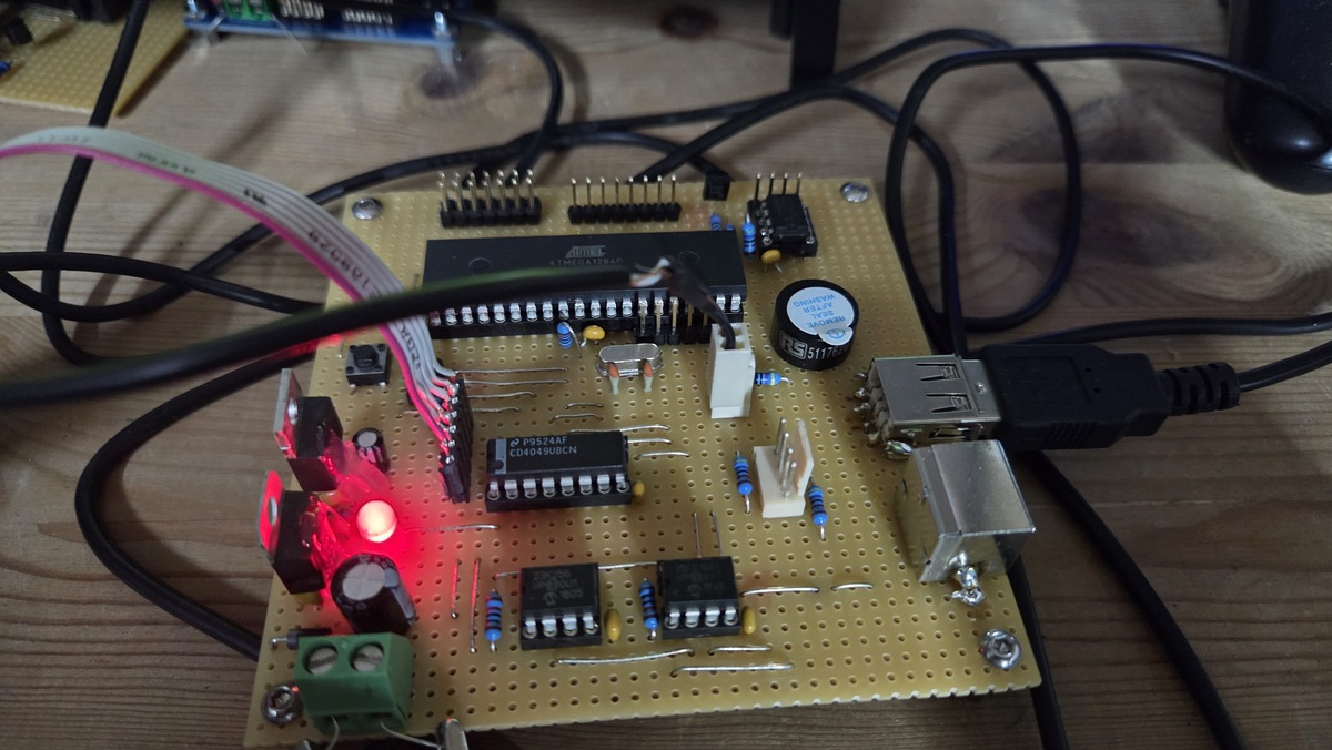
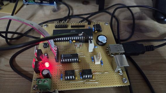
Selbstgebaute Platine mit ATmega-Mikrocontroller und Bauteilen
ATMEGA328P, CD4049UBCN, 10uF
in „AVR Tiny Basic Computer mit ATMega1284“ · Projekte & Code · · Platinenfotos
-
Bild
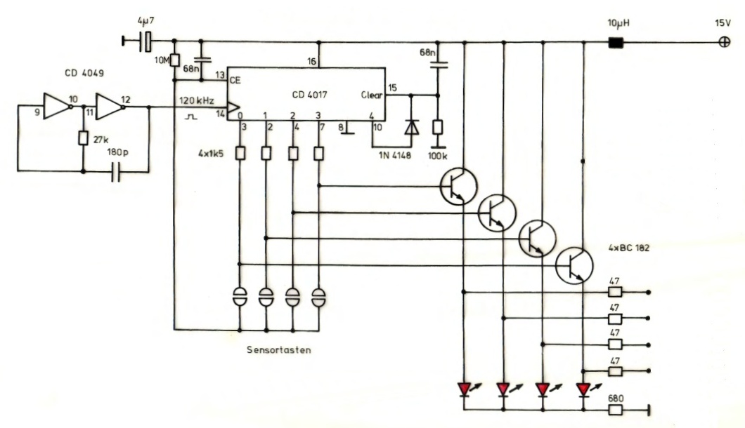
Schaltplan mit CD4019 und Transistoren
4µ7 10M 68n 13 CE 16 Clear 15V 15 CD 4049 10 12 9 11 27k 180p 120 kHz 14 0 1 2 3 4 4x1k5 3 2 4 7 8 10 1N 4148 100k 47 47 47 680 Sensortasten 4xBC 182
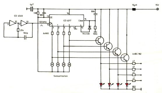
in „"Radio-Buttons" in TTL/CMOS-Logik“ · Mikrocontroller und Digitale Elektronik · · Schaltpläne
-
Bild
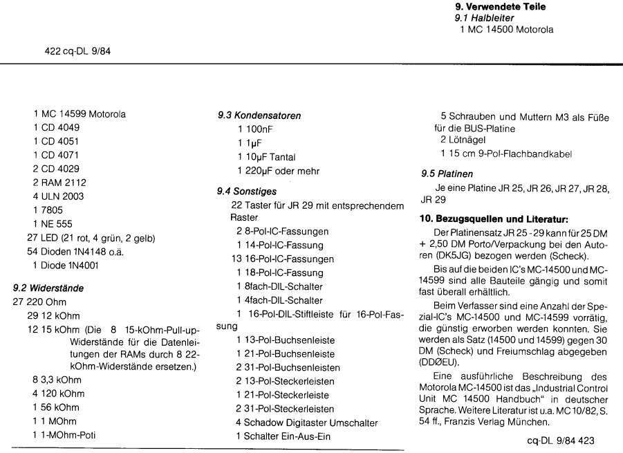
Teileliste für cq-DL 9/84 Projekt
9. Verwendete Teile 9.1 Halbleiter 1 MC 14500 Motorola 1 MC 14599 Motorola 1 CD 4049 1 CD 4051 1 CD 4071 2 CD 4029 2 RAM 2112 4 ULN 2003 1 7805 1 NE 555 27 LED 54 Diode 1N4148 9.2 Widerstände 27 220 Ohm 29 12 kOhm 12 15 kOhm 8 3,3 kOhm 4 120 kOhm 1 56 kOhm 1 1 MOhm 1 1-Mohm-Poti 9.3
in „Auftrag für Modellrechner“ · Analoge Elektronik und Schaltungstechnik · · Screenshots
-
PDF
cd4066b.pdf
Reset 15 CD4018B CD4018B 1 Q1 Q2 1 Q1 Q2 5 4 1 1/4 CD4066B 2 5 4 13 12 9 8 6 5 2 1 1 3 7 6 2 1/3 CD4049B 3 2 5 B 4 9 10 CD4001B 1/3 CD4049B 6 1 0 11 10 4 3 5 4 8 D C 10 9 Signal 12 6 5 13 12 6 5 11 Outputs 11 13 Channel 1 Signal 12 11 12 2 LPF Inputs Channel 1 1/6 CD4049B 10 N ▯ 1 2 1 Channel 2 5 4 CD4066B
in „Audi Delta mit Bluetooth per AM Taste“ · Fahrzeugelektronik ·
-
PDF
Understanding_Buffered_and_Unbuffered_CD4xxxB_scha004.pdf
inverters are rated at 2 unit loads (15 pF maximum). High-current unbuffered drivers, such as the CD4049UB, are rated at 3 unit loads (22.5 pF maximum). 14 Understanding Buffered and Unbuffered CD4xxxB Series Device Characteristics SCHA004 5 TA= 25°C 4 VDD = 15 V p VDD = 10 V – 3 I VDD = 8 V C 2 1 0 5
in „ungepufferten Inverter und gepufferten Inverter“ · Mikrocontroller und Digitale Elektronik ·
-
PDF
Messschieber.pdf
Die Intelligenz liegt dann im Tiger. Unser Konzept dazu ist folgendes: Ein 6-fach-CMOS-Inverter CD4049 als erste Stufe bildet einen AC-gekoppelten linearen Verstärker, der die Pegel von Clock und Data zunächst einmal reichlich verdoppelt. Leider funktioniert diese erste Stufe nur sicher bis zu einer
in „Anbaumessschieber Datenausgang“ · Mikrocontroller und Digitale Elektronik ·
-
PDF
Messschieber.pdf
Die Intelligenz liegt dann im Tiger. Unser Konzept dazu ist folgendes: Ein 6-fach-CMOS-Inverter CD4049 als erste Stufe bildet einen AC-gekoppelten linearen Verstärker, der die Pegel von Clock und Data zunächst einmal reichlich verdoppelt. Leider funktioniert diese erste Stufe nur sicher bis zu einer
in „Lidl "Workzone" Messschieber Protokoll ?“ · Mikrocontroller und Digitale Elektronik ·
-
Datei
Vergleichsliste_russ_CMOS.txt
?2 K561TR2 Quad 3-State R/S Latches CD4046B ??1561??1 KR1561GG1 Micropower Phase-Locked Loop VCO CD4049A ?561??2 K561L?2 6 Hex Inverting Buffers/Converters CD4050A ?561??4 K561PU4 6 Hex Buffers/Converters CD4050B ??1561??4 KR1561PU4 6 Hex Buffers/Converters CD4051A ?561??2 K561KP2 8-Channel Analog Multiplexer
in „Als Mikro noch Makro war: Die "Dicke Tal- Uhr"“ · HF, Funk und Felder ·
-
PDF
dac8512.pdf
30 is a method of generating a nega- 801 2049 –2.44E–3 800 2048 0 tive supply voltage using one CD4049, a CMOS hex inverter, operating on +12 V or +15 V. The circuit is essentially a charge 7FF 2047 +2.44E–3 000 0 +5 pump where two of the six are used as an oscillator. For the val- ues shown, the frequency
in „µC soll Strom rausgeben“ · Mikrocontroller und Digitale Elektronik ·
-
PDF
AN-339JP.pdf
range. on the order of ten to fifteen microseconds. This is however These devices are MM54HC4049/50, CD4049/50, and dependent on the way the IC was designed and the process- MM54C901/2/3/4. ing used. If standard logic is used and input voltages will exceed the In normal high speed systems noise spikes will
in „Induktionsspannung bei bistabilen Relais (1 Spule) direkt an Prozessor“ · Analoge Elektronik und Schaltungstechnik ·
-
PDF
657982_1.pdf
the 1MHz mode. OSC fOSC DEVICE TYPE The crystal and oscillator components should be located as 1 CD4049B Inverting Buffer 2 CD4070B Exclusive - OR close to the chip as practical to minimize pickup from other signals.Coupling from the EXTERNAL OSClLLATOR INPUT FIGURE 10. PRIMING CIRCUIT, SIGNALS A AND
in „Einen Gefallen tun“ · Mikrocontroller und Digitale Elektronik ·
-
PDF
ICM7216.pdf
to minimize pickup from other DEVICE TYPE signals. Coupling from the EXTERNAL OSClLLATOR INPUT 1 CD4049B Inverting Buffer to the OSClLLATOR OUTPUT or INPUT can cause undesir- 2 CD4070B Exclusive - OR able shifts in oscillator frequency. Display Considerations FIGURE 13. PRIMING CIRCUIT, SIGNALS A AND
in „[V] 1St. Harris ICM7216AIJI Ceramic DIP28 8-Digit, Multi-Function, Frequency Counters/Timers“ · Markt ·
-
PDF
ICM7226.pdf
this output will drive one DEVICE TYPE low power Schottky TTL load. When the buffered oscillator 1 CD4049B Inverting Buffer output is used to drive CMOS or the external oscillator input, a 10kΩ resistor should be added from the buffered oscillator 2 CD4070B Exclusive - OR output to VDD . FIGURE 15. PRIMING
-
PDF
PSpice_LibraryguideOrCAD.pdf
CD4041A CD4041A CD4000.OLB CD Buffer (Digital) CD4041UB CD4041UB CD4000.OLB CD Buffer (Digital) CD4049A CD4049A CD4000.OLB CD Buffer (Digital) CD4049UB CD4049UB CD4000.OLB CD Buffer (Digital) CD4050A CD4050A CD4000.OLB CD Buffer (Digital) CD4050B CD4050B CD4000.OLB CD Buffer (Digital) CD4503B CD4503B
in „pSpice - Bauteil hinzufügen.“ · Analoge Elektronik und Schaltungstechnik ·