-
Bild
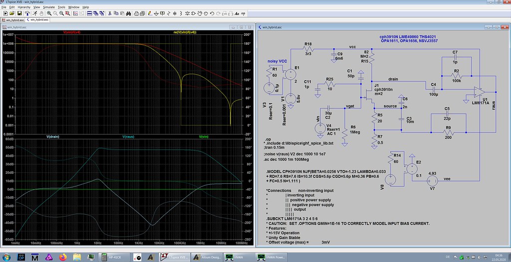
LTspice Simulation Schaltplan und Frequenzgang
cph3910N LME49860 THS4021 OPA1611, OPA1656, NSVJ3557 V(vin), V(drain), V(raus), R18, 3r3, vcc, E1, 60, C11, 1p, R25, 50p, J1, cph3910n, me2, drain, C4, 100k, R2, U1, LM6171A, noisy VCC, R1, 0.1u, V3, Rser=1, 1V, 30u, vgat, C2, 2n
in „Unbekannte Funktion in low-noise Amp“ · Analoge Elektronik und Schaltungstechnik · · Screenshots
-
PDF
micromachines-13-01381-v2.pdf
input to the operational amplifier is limited to 0 ▯ 5 V. The noninverting amplifier constructed by OPA1611 is used to amplify the signal by 11 times, which is mainly used to improve the signal-to-noise ratio of the input signal during low-power power transmission. In addition, the noninverting amplification
-
PDF
EKG_usw_Informationformedicalapplications_von_TI.pdf
channels. OPA380 Digital OPA380 Output Multiplexer ADS8383 OPA380 CT scanner application using the OPA380 and the ADS8383. The DDC112 is a complete two-channel solution for measuring photo- from 50 pC to 1000 pC.
in „EKG Schaltung Neuling“ · Analoge Elektronik und Schaltungstechnik ·
-
PDF
Last_board_mixed.pdf
R402 5 K401 P Q401 5 VIN-REF 3 O R403 IXFB210N30P3 , t 1 kOhm 0Ohm 1 G 1 0 t 4 10Ohm S 3 0 n C401 2 OPA735AIDBVT 1 b B 5 0 B 100pF np 0 5 SHUNT-FEEDBACK IC402 0 o V 1 8 3 = g N P 2 IN- IN+ 7 3 * u G 5 O 3 GND REF1 6 + 2 1 R r A - 4 REF2 VS 5 = t NC OUT 1 2 1 h U e N INA240A2DR 4 O o V G B 4 3 0 v n A
in „Schaltplankontrolle Last- + HMI-Board“ · Mikrocontroller und Digitale Elektronik ·
-
PDF
MCP41HVX1.pdf
A. The V+ AW VD MCP41HVXX Common A and Common B connections could be + connected to V+ and V-. D 1 OPA170 A - Common A R1 B R2 Input V+ A + OPA170 V - OUT To base W of Transistor FIGURE 8-4: High Voltage DAC. (or Amplifier) EQUATION 8-1: DAC OUTPUT VOLTAGE CALCULATION 8-bit B N R1 VOUT(N) = 255 x (DV
in „MCP41HVX READCMD falsch verstanden??“ · Mikrocontroller und Digitale Elektronik ·
-
PDF
pm2534ocr.pdf
clock pulses for the result of an ADC cycle: SS in, a — — — — — — — r e W A I T t-SU TO- P» 2 OTt N oePA Tz- PP|+AW A I T - S T A T E t ST99 S T A R T 8 6 0 2 2 8 Figure 3.21 If the ADC control is in the WAIT-state a start can be generated and the ADC control starts the UP-phase. The timing of the UP<phase
in „Pjilips PM2519“ · Markt ·
-
PDF
apple_macbook_pro_a1286_mlb_d1_051-9216_13.3_retina_a1425_820-3462_sch.pdf
=TRUE TRUE 7 17 I1968 USB3_EXTB_RX_RC_P I1975 TRUE CON_DMIC_SDA1 55 I1669TRUE DP_INT_AUX_P 67 79 I1611 TRUE LPCPLUS_RESET_L 25 41 TRUE PCIE_AP_R2D_P 36 75 MAKE_BASE=TRUE TRUE TP_LPC_DREQ1_L USB3_EXTB_RX_RC_N TRUE I1976 TRUE CON_DMIC_CLK 55 I1668TRUE DP_INT_AUX_N 67 79 I1610 TRUE SMC_TDO 39 40 41 TRUE
in „Macbook Schaltpläne“ · Mikrocontroller und Digitale Elektronik ·