
Cypress USB HUB Chip Schaltplan

Gast #3777309
Lesenswert?

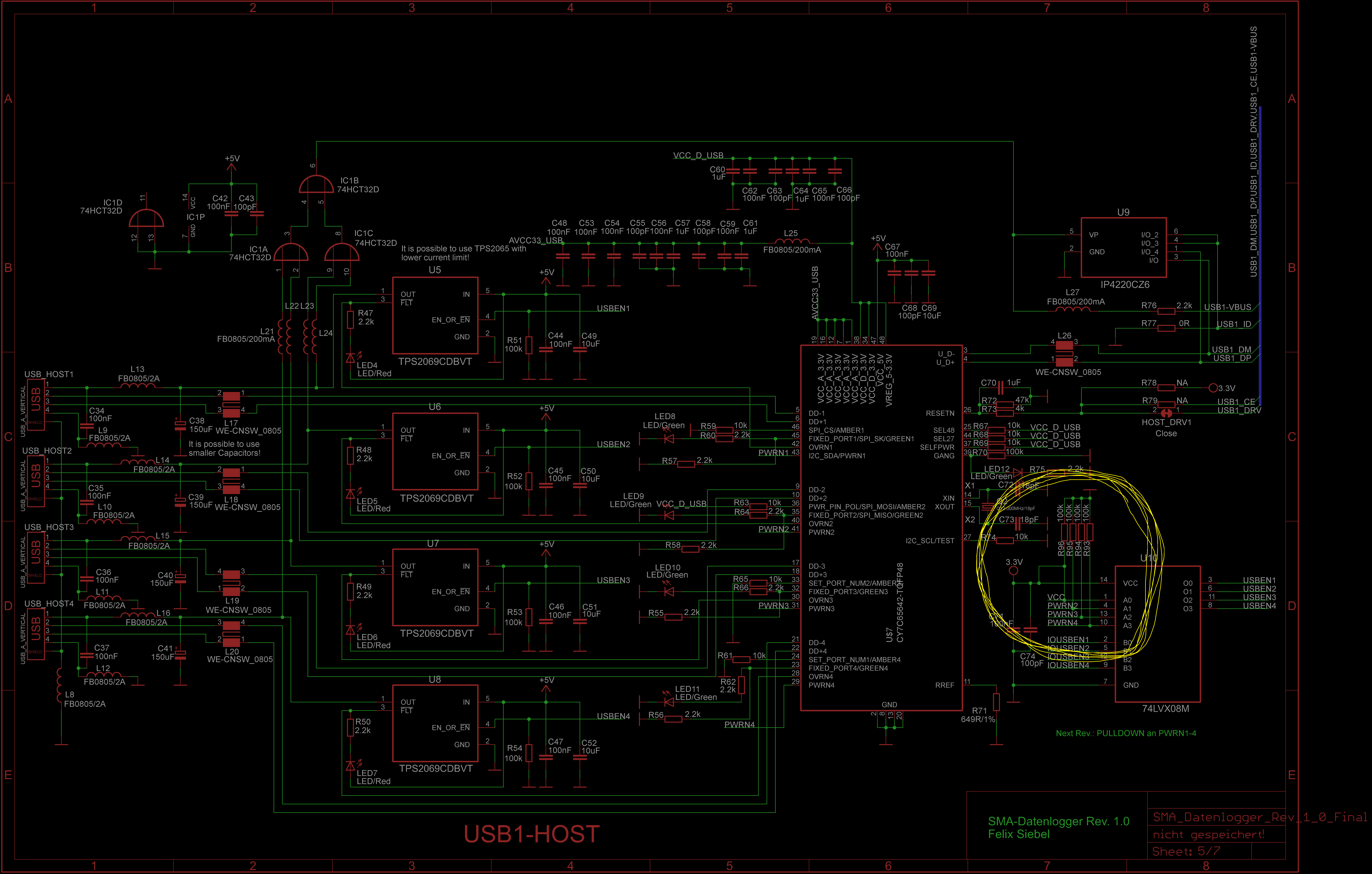
Könnt Ihr mal über den Schaltplan schaun?

Bin mir da nicht so sicher mit dem Reset Pin vom Chip. Der geht halt an 
3.3V USB_DRVV von nem AM3352. Sollte ja eigentlich funktionieren oder?

Auch meine Konstruktion um jede Buchse einzeln abschalten zu können. Die 
Pins IOUSBEN werden von GPIO Pins beim Booten bevor USB aktiviert wird 
auf High gezogen.. Dürfte ja dann keine Probleme machen beim Kernel 
booten oder?


Leider hab ich aber irgendwie Probleme. Der Chip wird vom Linux nicht 
erkannt. Komisch ist, das manchmal die TPS Chips bereits an sind obwohl 
der USB Chip noch mit Reset auf GND liegt. Sind die Pulldowns bei den 
TPS vielleicht zu klein?
Angehängte Dateien:
Gast #3778344
Lesenswert?

Hi,

i got it to work. But with a really strange hack.

I marked it with the Yellow Circle in the attached schematic.

Also it doesn't matter to which PWR# Pin (PWRN1 PWRN2 PWRN3 PWRN4) i 
connect the 3.3V.

I also tested it with a 4k2 and a 2k2 Resistor Pullup without R93 -R96. 
It doesn't work with a resistor between.

Directly wired to 3.3V it works and Linux enumerates everything.

I thought it could be a Voltagesource thing. I measured all source Pins 
from the CY7C65642 and the U10 74LVX08M Chip but all Voltage level are 
looking fine. Everything is at 3.3V  (tought it is possible that the 
voltage drops if the Chip couldn't get enough current).

I measured also the Delay between the 5V Source is coming uo and the 
3.3V Soure (Not the intern regulated!!) It is a schort delay of 25-25 
ms.

Also i desoldered C70 (Reset Pin). To get the response to the USB_DRV 
Signal faster.

Could you give me some advise for this strange behaviour?
Angehängte Dateien:

Antwort schreiben

Bitte melde dich an, um einen Beitrag zu schreiben.

oder

Mit Google-Account einloggen

Die Registrierung ist kostenlos und dauert nur eine Minute.

Jetzt registrieren