Gast
#4124211
Hello people!

I am wondering about how is the impedance output of the I/O pins of this
FPGA. I have been reading the datasheet and I don't understand what is
the meaning of the On Chip termination resistance and how to configure
this option in a proper way.

First of all I am using an I/O standard 3.3-V-LVTTL and reading the
"Termination Scheme for I/O Standards" of the datasheet:

"The 3.3-V LVTTL, 3.0-V LVTTL and LVCMOS, 2.5-V LVTTL and LVCMOS, 1.8-V
LVTTL and LVCMOS, 1.5-V LVCMOS, 1.2-V LVCMOS, 3.0-V PCI, and PCI-X
I/O standards do not specify a recommended termination scheme per the
JEDEC
standard"

So it means that I can not use an OCT with this kind of I/O standard
right? or what does it mean?

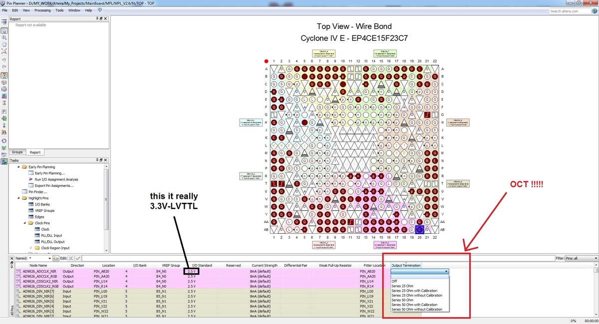
On the other hand having, the track in the PCB is routed to be in
compliance with 50 Ohm requirements. So in the picture attached should I
choose the termination option 50 Ohm right? Does it mean that I will put
an internal source resistance in the FPGA I/O, right?

Thanks
Angehängte Dateien:
-
 Quartus_II_OCT.jpg
(240 KB)
Quartus_II_OCT.jpg
(240 KB)