
Hallo, ich soll Pad auf die Cutout von Board liegen. Aber wenn ich die
Pad mit dem Draht verbinden. Es berichtet immer circuit short Fehler und
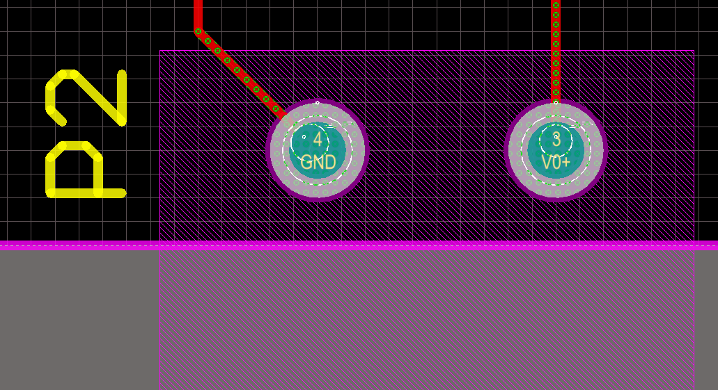
auch clearance constraint. Im Bilder Links ist die PCB. P2 ist eine
connector mit Pad3 und Pad4 mit Radien von 0,5mm. Unter Pad3 und Pad4
sind 2 Board cutouts auch mit Radien von 0,5mm.
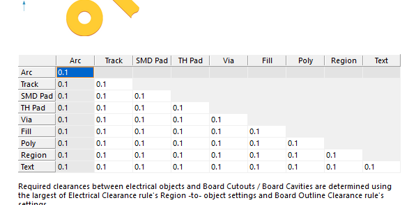
Das andere Bild ist die Rule von die clearance.

Eine Verbindung mit diese Pad und andere Komponente wird immer circuit
short machen.
Kann mir jemand helfen?

Vielen Dank im voraus!
Gast
#4902000
Do you have an airline, if you delete the last (green marked) part from
the track?

To place a pad above a (board?)cutout is bullshit, how should it work?
Or did I understand you wrong?
You've understood. The Board has some through holes nearby the edge. And
the connector were then planed to be put above the holes.
There is airline between the pins.

Could you give me some advice if I should put the connector(header)
above the holes.
I think I can delete the holes, and then just put the pads(also the
connector) at the right location of the holes. Is that OK?

Thanks a lot!
Gast
#4904754
You cant place a pad above a board cutout. Boardcutouts is for something
like holes or rips. Your try to place your pad into the air.

Is it realy the clearence roule, which you violate? What did DRC report?
Its seems not plausible for me, that your posted clearence rule is
violated. Altium marks some violations white, the white circles in the
pads are such marks. It doesnt looks like clearence violation, but I
cant interpret it only from your picture.

But short circuit would be plausible. I dont know your schematic or
netlist, if it would not be to obviously I would guess, you had
connected the wrong pads to the wrong tracks.
Antwort schreiben
Bitte melde dich an, um einen Beitrag zu schreiben.