to ground See Figure 4 60 ns R with 100 kΩ to ground 370 S r Differential output signal rise time 25 50 100 ns V(Rs)= 0 V f Differential output signal fall time 40 55 80 ns r Differential output signal rise time 80 120 160
Output voltage drop V @ 50 mA 0.4 0.4 0.4 0.4 Output current (sinking) mA 50 50 50 50 Output leakage with no input microamps @ 100 100 10 100 30 VDC Transistor V breakdown 30 30 30 30 Temperature: Operating °C –30 to +70 –30 to +
einfachen Taster die Relays kurz ansteuern um die dann 15 sekunden ( gut eingestellt ist es auf 2x6s sek aber 12s würden auch reichen) eingeschaltet lassen. Ich bin nicht drauf gekommen wozu das Ding da ist. Ausser es verhindert irgendwie, dass man zb bereits nach 5s die andere taste drückt und dann
das steht auf dem Zettel zwischen W und R = 25,6 Ohm und ziwschen W und S = 24,2 Ohm und zwischen S und R = 48,4 Ohm
gegossen hast. Nö. Man nehme den [[Royer Converter]], zwei Halbschalen und Spulen. Dazwischen 1,5mm FR4, das hat ca. 40kV/mm Durchschlagsfestigkeit. Der Koppelfaktor ist unkritisch, kann man kapazitiv kompensieren. Been there, done this, bis 60kV Isolationsspannung ;-)
erfahrene Leute was dazu sagen. Der von mir vorgeschlagene Wander RHV2 ist getestet mit 20kV DC, 1s 12,5kV AC / 50Hz, 1min Außerdem ist er mit max. 4pF Koppelkapazität spezifiziert, d.h. der ist für sehr schnelle Schaltvorgänge an H-Brücken zur Versorgung der High Side gedacht. Dafür sind die 1400VRMS
Ich würde 1S xP, ein oder mehrere LiPo Zellen parallel und mit einem briefmarkengroßen StepUp Modul vom Chinesen arbeiten, um auf die 12V zu kommen. 120mA bei 12V sind bei 3V 480 mA und 3V ist schon untere Grenze
................................................................................................10 mA at 5 V DC Switch Travel S (Standard) ..................................................................................................................................................................
General Description 2. Features RH6016 is 1 channel capacitive touch detection IC, Operating voltage:2.4V~5.5V which can take the place of mechanical switch or Operating current (@VDD=3V no load): button. 10uA at low power mode RH6016 built in high precision regulatPOR、 LVR、 Finish initial in 0.5s after
Output (Float) 0℃≤T ≤A5℃,I BAT40mA 4.137 4.2 4.263 V Voltage BAT Pin Current R PROG = 2.4k, Current ● 450 500 550 mA Mode Text condition:VBAT=4.0V R PROG = 1.2k, Current ● 950 1000 1050 mA BAT Mode Standby Mode, VBAT= 4.2V ● 0 -2.5
A V V P A ( sA7 1 32 A14 c t A6 A13 d u A4 A9 r o A3 9 M27C2001 25 A11 P A1 A10 te A0 E o le Q0 17 Q7 b s 1 2 S 3 4 5 6 O Q Q V Q Q Q Q AI00718 6/25 Summary description M27C2001 Figure 4. TSOP Connections A11 1 32
5: Typ. output characteristics Diagram 6: Typ. drain-source on resistance 80 12 4.5 V 5 V 6 V 10 V 60 8 ] 5.5 V ] [ 40 4.5 V [ 6 V I n S 7.5 V D 10 V R 4 20 4 V 0 0 0 1 2 3 0 10 20 30 40 50 V DSV] D [A] ID=f(VDS; Tj25 °C; parameter: V GS RDS(on)f(D );jT=25 °C; parameter: VGS Diagram
Spannungsabfall bei 500mA: - https://www.reichelt.de/de/de/shop/produkt/schottky-gleichrichterdiode_40_v_20_a_axial_5_4_x_7_5_mm-276728
Spannungsabfall bei 500mA: > - > https://www.reichelt.de/de/de/shop/produkt/schottky-gleichrichterdiode_40_v_20_a_axial_5_4_x_7_5_mm-276728 Die Idee mit den Mosfets kam daher, dass ich die Vf heruntersetzen wollte, denn die Anschlüsse geben ja nur 5V. Wenn ich da noch zb 0,3V abziehe, bleibt nicht mehr
Oliver S. schrieb im Beitrag #8035449: > Nach DIN 18014 darf der (Fundament-) Erder nur durch eine > Elektrofachkraft ERSTELLT werden. Das ist eine Norm, nein Gesetz.
Udo S. schrieb im Beitrag #8036903: > Thomas schrieb im Beitrag #8036897: >> Ein üblicher "B" LS schaltet innerhalb von ca. 0,01 - 0,1s ab. Das setzt >> aber einen entsprechenden Kurzschlußstrom voraus
Raum zu reisen! https://youtu.be/tKpsrhLv-jw?si=dEtU5_bL59rDJGhS
bereits knapp: https://de.wikipedia.org/wiki/Turing-Test#Durchgef%C3%BChrte_Turingtests_und_%C3%A4hnliche_Tests "Im März 2025 wurden in einer Studie vier Systeme (ELIZA, GPT-4o, LLaMa-3.1-405B und GPT-4.5) in zwei randomisierten, kontrollierten und vorab registrierten Turing-Tests mit unabhängigen
VITRIP ITRIP−VSS −0.3 to +10.0 V Operating Junction Temperature Tj 150 _C Storage Temperature Tstg −40 to +125 _C Module Case Operation Temperature Tc −40 to +125 _C Tightening Torque MT Case mounting screws 0.6 Nm Isolation Voltage Viso 50 Hz sine wave AC 1 minute (Note 4) 2000 Vrms Stresses exceeding
3.88 inch display for easier maps, messaging, and app navigation • Quad core hardware with 4 GB RAM and 64 GB storage running Android 12 • Worldwide 4G support where available for on grid use • Optional prepaid 2 GB data SIM for hybrid operation with no contracts • Power efficient
[code] It's important for the project as whole to be able to move forward and rely on modern tools and technologies and not be held back by trying to shoehorn modern software on retro computing devices. [/code
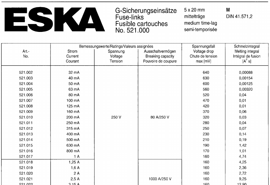
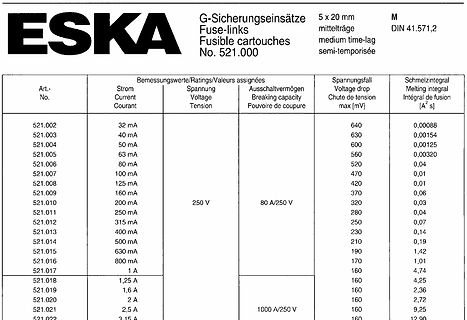
Spannungsabfall Voltage drop Chute de tension max [mV] Schmelzintegral Melting integral ∫ fusion [A²s] 521.002 32 mA 640 0,00088 521.003 40 mA 630 0,00154 521.004 50 mA 600 0,00125 521.005 63 mA 560 0,00320 521.006 80 mA 520 0,04 521.007 100 mA 470 0,01 521.008 125 mA 420 0,01 521.009 160 mA 370 0,06 521.010 200 mA 250 V 80 A/250 V 320 0,03 521.011 250 mA 280 0,04 521.012 315 mA 250 0,07 521.013 400 mA 230 0,14 521.014 500 mA 210 0,19 521.015 630 mA 190 1,42 521.016 800 mA 170 1,01 521.017 1 A 160 4,74 521.018
= 50 A iss e 8 VDS= 30 V F 10 000 a ( 1000 o 1000 e C oss V n n e e e e 6 e l i l l l u l na 1000 s n d o s 2pa 1 2 2 - 4 1 C - - 100 t 100 C 100 C rss G - 2 G V 10 10 0 10 0 10 20 30 40 50 60 0 40 80 120 160 200 VDS - Drain-to-Source Voltage (V) Qg- Total Gate Charge (nC) Capacitance Gate Charge S21
rise more quickly, producing a narrower (h) 5.2 Luminance and earlier burst pulse (starting approx. 0.4 s after sync and Output about 0.6 s wide). The burst will be wider and later if the (Pin6) resistor is raised to 62 k , but more importantly, the 5.0 V 4.3 reset point may not be reached in one full
7 10 A 8 16 A ) * /61 cURus Zulassung 2 OA 5671, 72, 81, 82 / 06.06.24 de / 882A Kennlinien 2,2 _ 4 1,0 b 2,0 M 0,9 5 UB max. 0,8 M 1,8 ohn Last 0,7 1,6 0,6 UB max. 1,4 bei I max. o 0,5 k s 0,4 U B 1,2 t UN u 1,0 e 0,3 R 0,8 0,6 0,2 0 20 40 60 80 100°C 0,2 0,4 0,6 0,8 1 Umgebungstemperatur Leistungsfaktor
Vj b b i t> > O 3 .U .O (0 >*-J -i •-) uW E M0 ) _ d C d 4 - i H 4 - 4 J S - i 3 i j jr IQ W B CQ u 3 d) c: e a x „ 1 d -U o) 4-i 4-1t») J3 .0 .0 .0 OJ ^ DUCd ) O D 0) d U U d) -C ,X C -C J3S C d O r ß H U 05.-H U dl S o J d J S t I 5 o f l 5 ^ H H O •0 Q d
Ich muss ja beim Anliegen des TE an Beggar's Opera denken...
40 gerissen. Und ich lass die Leute halt ihr Ding machen, solange ihr Ding nicht ist, anderen ihr Ding verbieten zu wollen. Udo S. schrieb im Beitrag #7948940: > Ich bin ziemlich weiß, eher alt und
This chip integrates a 128 MHz arm-cortex M33 processor, an RISC-V coprocessor, and a power-saving 2.4 GHz multiprotocol radio chip. The Bluetooth LE 6.0, Matter, Thread, Zigbee, NFC, and IEEE 802.15.4 radio protocols can be used, as can also proprietary 2.4 GHz protocols. . . . [/c] ### Phoenix
> Microchip maXTouch - Zwei-Seiten-Touchscreen > Am Stand von Microchip zeigte man einen Touchscreen, der dank geschickter > Polarisierung je nach Einfallswinkel des Betrachters unterschiedliche Inhalte > präsentierte
BLOCK DIAGRAM R L U Vo o U 7 Vi µ V µ i 0 2 2 V E 0 0 M 0 1 1 F 1 F 2 5 2 . 2 1 . 0 R k + A + 7 R 0 4 D 4 k - T 5 k 4 F 1 6 9 4 3 . - i 1 6 k F u F E r 8 A NC n c 6 4 G AH 4 n e t 1 O u s S T 8 m t n O E s . 4 4 E E N E a 6 7 7 L M D 0 f d k U R 4 p o e 0 ) P F O u t C 1 1 L EH 7 V o e C O Tk s e H 2 F3 a l ( 2 k , v k E + t l 0 NR 6 n I C 1 1 O EO 0 n m N E N EC 4 p 1n o f S E L FT 5 ht di wegapll uf , koobdpah k k S B EE m 2 2 7 TD C T 1 F o 1 I N N 0 µ l z R R 4 0 µ a N H E R 1 r o E 8 H 8 E C e r a I 1 T 3 I R x t i I O e s i V S L k h o E R 0 i 1 T E G Z 1
tGLQX Output enable low to output transition 5 5 5 ns tEHQZ Chip enable high to output Hi-Z 25 35 40 ns tGHQZ Output enable high to output Hi-Z 25 35 40 ns tAXQX Address transition to output transition 10 5 5 ns 1. Valid for ambient operating tempeAature: T = 0 to 70 °C orCC= 4.75 to 5.5 V or 4.5 to
kn to 7 kn Vee+= 13.2 v, Data input 1 10 l1H High-level input current 3 V e e -= -13.2 v, µA V1=2.4V Strobe input 2 20 Vee+= 13.2 v. Data input -1 -1.6 l1L Low-level input current 3 V e e -= -13.2 v, mA Strobe input - 2 -3.2 V1=0.4 V V o = 25 V 2 Short-circuit output current V cc+=13.2v. V o = -2 5 V - 3 las 4 V e e -= -13.2 v V o = O V , V 1 = 3 V 15 mA V o = O V ,V 1 = 0 V -1 5 Vee+= 13.2 v, V e e -= -13.2 v. iccH+ Supply current from Vee+. high-level output 10 22 mA 5 V1 =O V, RL = 3 kH, ic c H -Supply
27 EZ-USB™ HX2VL low-power multipletransaction translator USB 2.0 hub controller Pin configurations 4 Pin configurations I A X G M D R P S B _ P E 2 W O P O E P R P I N S C # V W V V L V I [ O S [ E _ [ # # # G C P E C C ] R K ] L D ] [ [ [ N _ W G C S / 1 / / 7 A / ] ] ] G D R 4 4 4 4 4 4 4 4 4 3 3
temperature PARAMETER TEST CONDITIONS MIN TVP MAX UNIT Iv Luminous Intensity (See Note 2) V ee= 5 v. IF= 10 mA 40 110 µcd hp Wavelength at Peak Emission 640 655 670 nm ~;\ V ee= 5 v, V L E o= 4V Spectral Bandwidth 20 nm V1H High-Level Input Voltage 2 v V1L Low-Level Input Voltage 0.8 v V1K Input Clamp Voltage V ee= 4.5 v, 11 = -1 2 mA -1 .5 v l1H High-Level Input Current V ee= 5.5 v, V1=2.4 V 150 µA l1L Low-Level Input Current V ee= 5.5 v, V1=0.4 V -1 mA Irow Row Input Current l Row 1 thru Row 6 500 800 J Row7 See
Supply Figure 25. FB Threshold Voltage vs Temperature Voltage 8 8 Ω H ] O7 [7 : N e R n6 :6 s VCC=3.5V c s5 t5 R i N e O4 R4 VCC=3.5V i O S e i3 i3 H w u o t2 VCC=12V t2 O t u1 1 O VCC=12V 0 0 -40 -20 0 20 40 60 80 100 120 -40 -20 0 20 40 60 80 100 120 Temperature [˚C] Temperature [˚C] Figure
n e 2 4 F F u a 6 0 7 0 W o C 1 C 1 5 r 4 I . a D D d , l T % o 1 1 5 P T 0 R T e r 7 R 1 a s k 3 0 3 1 3 1 2 s o 9 0 D N D N D N C o c R 3 1 1 1 Q M i a 4 4 e a D 4 D 4 F r c 8 k 1 1 μ a a R 1 5 . * * C 0 s
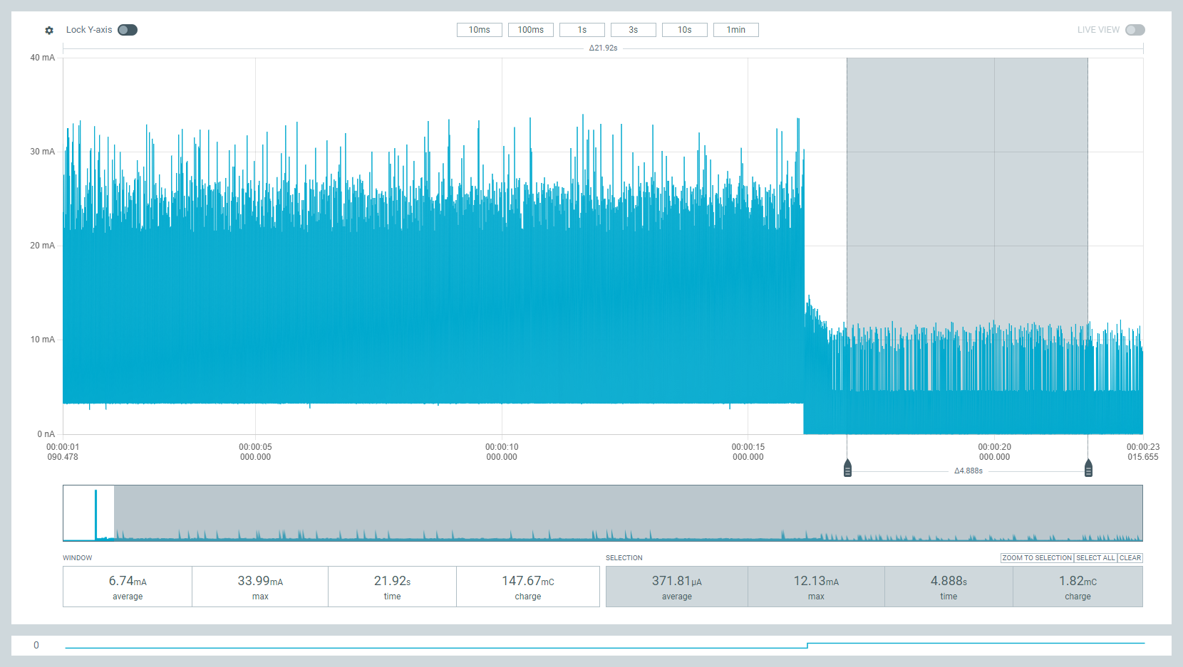
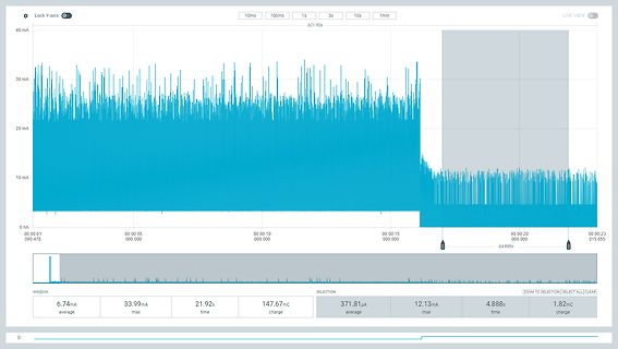
Lock Y-axis 10ms 100ms 1s 3s 10s 1min LIVE VIEW 40 mA 30 mA 20 mA 10 mA 0 nA 00:00:01 00:00:05 00:00:10 00:00:15 00:00:20 00:00:23 090.478 000.000 000.000 000.000 015.655 WINDOW SELECTION ZOOM TO SELECTION SELECT ALL CLEAR 6.74mA average 33.99mA max 21.92s time 147.67mC charge 371.81µA average 12.13mA max 4.888s time 1.82mC charge
工作温度 Topr –40~85 ℃ working temperature 存储温度 Tstg 5~30 ℃ Storage temperature 焊接温度 Tsld 回流焊 260℃不超过 30s ℃ welding temperature Reflow soldering 260 ℃ not more than 30s 手动焊接 300℃不超过 3s Manual welding at 300 ℃ for no more
.......65 6 / 67 W5500 Datasheet Version1.1.0 Pin Assignment E E E D D D D D D D D D n G C C M M M S S S S S S A N N P P P R R R R R R 4 4 4 4 4 4 4 4 4 3 3 3 TXN 1 36 INTn TXP 2 35 MOSI AGND 3 34 MISO AVDD 4 33 SCLK RXN 5 32 SCSn RXP 6 31 XO W5500 DNC 7 30 XI/CLKIN AVDD 8 48LQFP 29 GND AGND 9 28 VDD
- mA can be determined by using the minimum value for K1 (0.005) and the normalization factor from Figure 4.The example is to determine I 1 (min) for the condition of K1 at T =75°C, and The servo gain is
g u 0 n l t r p t n t t t t e k 1 2 a / N T A i a a a a a e i i n e z S S S S S e B B A P B B 1 2 Bauteil 74xxxx 74HC374ADW SMD 8BitFlipFlop 24 0,30€ 3 Bauteil 74xxxx 74HCT161 SMD Counter 30 0,70€ 4 Bauteil 74xxxx 74150 Multiplexer,Decoder 21 3,00 € 5 Bauteil 74xxxx 74168
Qrlg.lSlze Unterlagennummer/ Reference IoA/Ed. Benennung/Nomencloture Ilem Cop + - "'eid fur Kurz.-And 1 4 4 322-49.0001.0089 BI. : 1 A5 In h a lts v e rz e ic h n is . 2 3 4 010-40.1004.0208 BI. : 1 A2 Maßzeichnung 3 4 4 309-48.3101.0310 B l.:1 -4 A2 K urzbeschreibung 4 4 4 300-40.1004.5006 BI. : 1 Al S
557 Philips Semiconductors Linear Products Product specification CMOS 8-bit A/D converters ADC0803/4-1 AC ELECTRICAL CHARACTERISTICS ADC0803/4 SYMBOL PARAMETER TO FROM TEST CONDITIONS UNIT Min Typ Max Conversion time fCLK =1MHz 1 66 73 s 1 fCLK Clock frequency 0.1 1.0 3.0 MHz Clock duty cycle 1 40 60
Reverse bias safe operating area CE RBSOA Square - Short circuit safe operating area VCE = 400 V SCSOA 4 - - μs Allowable offset voltage slew rate U to NU, V to NV, W to NW dv/dt 50 - 50 V/ns Driver Section VBS = 15 V (Note 4), per driver ID - 0.07 0.4 mA Gate driver consumption current V = 15 V, total

 Bild
Bild
 Bild
Bild
 Bild
Bild