rise more quickly, producing a narrower (h) 5.2 Luminance and earlier burst pulse (starting approx. 0.4 s after sync and Output about 0.6 s wide). The burst will be wider and later if the (Pin6) resistor is raised to 62 k , but more importantly, the 5.0 V 4.3 reset point may not be reached in one full
Raum zu reisen! https://youtu.be/tKpsrhLv-jw?si=dEtU5_bL59rDJGhS
bereits knapp: https://de.wikipedia.org/wiki/Turing-Test#Durchgef%C3%BChrte_Turingtests_und_%C3%A4hnliche_Tests "Im März 2025 wurden in einer Studie vier Systeme (ELIZA, GPT-4o, LLaMa-3.1-405B und GPT-4.5) in zwei randomisierten, kontrollierten und vorab registrierten Turing-Tests mit unabhängigen
. Versand Es handelt sich um * 10 Stück mit 2 x 48 V / 100mA * 08 Stück mit 2 x 18 V / 139 mA * 09 Stück mit 2 x 09 V / 278 mA Hersteller unbekannt Gruß Holger
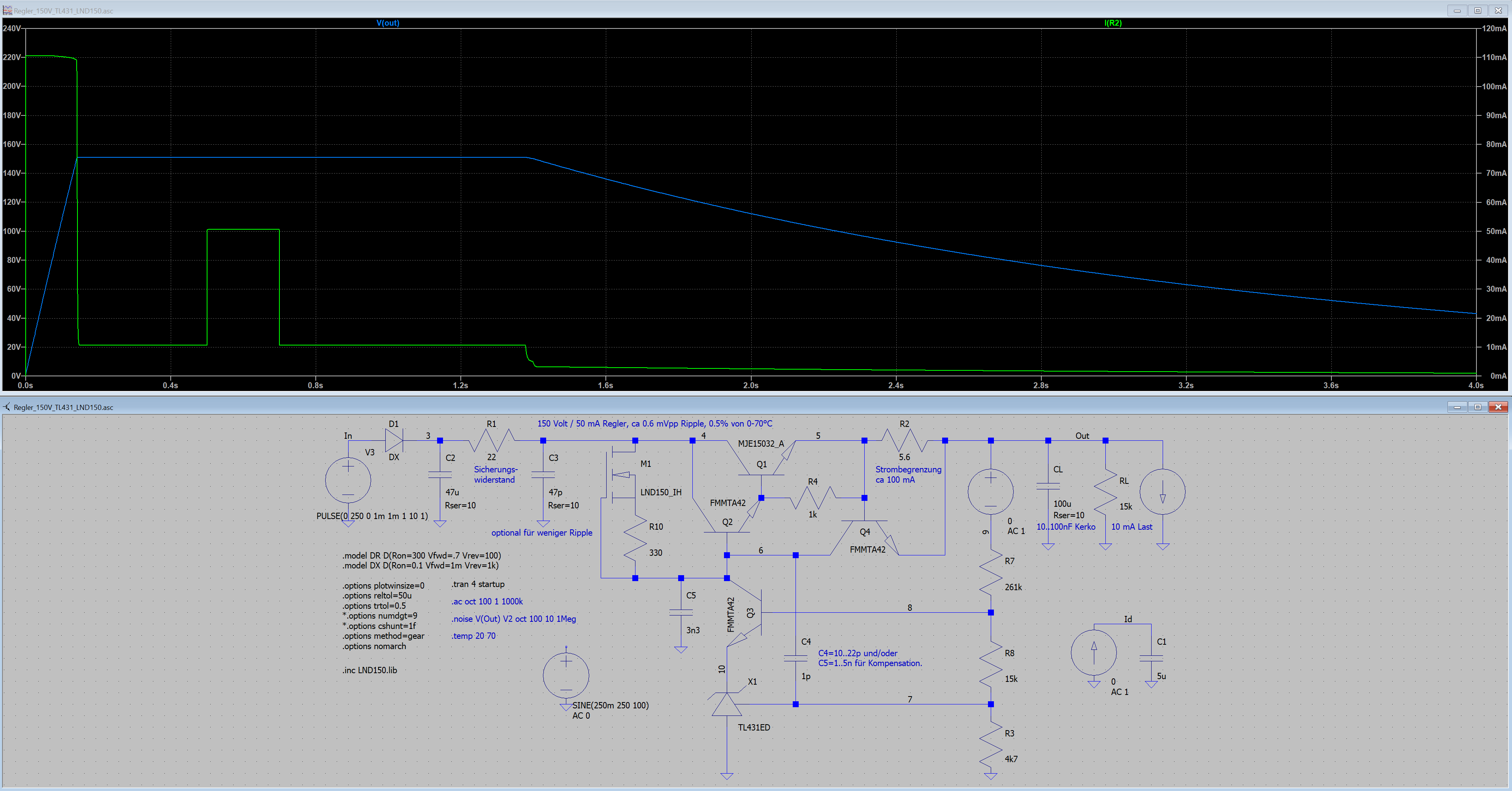
der Längsregler 4,5% mehr an Eingangsspannung. Das muss dann in Wärme umgesetzt werden.
7 10 A 8 16 A ) * /61 cURus Zulassung 2 OA 5671, 72, 81, 82 / 06.06.24 de / 882A Kennlinien 2,2 _ 4 1,0 b 2,0 M 0,9 5 UB max. 0,8 M 1,8 ohn Last 0,7 1,6 0,6 UB max. 1,4 bei I max. o 0,5 k s 0,4 U B 1,2 t UN u 1,0 e 0,3 R 0,8 0,6 0,2 0 20 40 60 80 100°C 0,2 0,4 0,6 0,8 1 Umgebungstemperatur Leistungsfaktor
BLOCK DIAGRAM R L U Vo o U 7 Vi µ V µ i 0 2 2 V E 0 0 M 0 1 1 F 1 F 2 5 2 . 2 1 . 0 R k + A + 7 R 0 4 D 4 k - T 5 k 4 F 1 6 9 4 3 . - i 1 6 k F u F E r 8 A NC n c 6 4 G AH 4 n e t 1 O u s S T 8 m t n O E s . 4 4 E E N E a 6 7 7 L M D 0 f d k U R 4 p o e 0 ) P F O u t C 1 1 L EH 7 V o e C O Tk s e H 2 F3 a l ( 2 k , v k E + t l 0 NR 6 n I C 1 1 O EO 0 n m N E N EC 4 p 1n o f S E L FT 5 ht di wegapll uf , koobdpah k k S B EE m 2 2 7 TD C T 1 F o 1 I N N 0 µ l z R R 4 0 µ a N H E R 1 r o E 8 H 8 E C e r a I 1 T 3 I R x t i I O e s i V S L k h o E R 0 i 1 T E G Z 1
kn to 7 kn Vee+= 13.2 v, Data input 1 10 l1H High-level input current 3 V e e -= -13.2 v, µA V1=2.4V Strobe input 2 20 Vee+= 13.2 v. Data input -1 -1.6 l1L Low-level input current 3 V e e -= -13.2 v, mA Strobe input - 2 -3.2 V1=0.4 V V o = 25 V 2 Short-circuit output current V cc+=13.2v. V o = -2 5 V - 3 las 4 V e e -= -13.2 v V o = O V , V 1 = 3 V 15 mA V o = O V ,V 1 = 0 V -1 5 Vee+= 13.2 v, V e e -= -13.2 v. iccH+ Supply current from Vee+. high-level output 10 22 mA 5 V1 =O V, RL = 3 kH, ic c H -Supply
wurde die geflogene 4A Sicherung ersetzt und auf 3. Kurzschlüsse gemessen, die nicht vorhanden sind. 4. Wärmebildkamera raus - eingeschaltet - und nach 10-15 Sek. und 70°C - zur Sicherheit abgeschaltet, bevor die Sicherungen
ich für das obige Beispiel den hier im Auge: https://www.reichelt.de/de/de/shop/produkt/printtrafo_4_8_va_12_v_400_ma_rm_25_mm-2463 Aber 2V mehr könnten evtl. schon Probleme verursachen. Hab mich jedenfall nicht getraut - auch wenn es beim Test funktionieren mag - aber wie sieht es in ein paar Wochen
-ma-schaltpositionen-12-15-1-st.pdf So kenne ich die Preise, früher auch offen aus hellem Pertinax.
nicht das Problem, Bin dabei Kalibrierkoffer zu bauen, in diesen Fall für L/C und R, natürlich in 4 pol Technik. Kalibrierkoffer für HV/ISO und PE bereits fertig. Danke
Supply Figure 25. FB Threshold Voltage vs Temperature Voltage 8 8 Ω H ] O7 [7 : N e R n6 :6 s VCC=3.5V c s5 t5 R i N e O4 R4 VCC=3.5V i O S e i3 i3 H w u o t2 VCC=12V t2 O t u1 1 O VCC=12V 0 0 -40 -20 0 20 40 60 80 100 120 -40 -20 0 20 40 60 80 100 120 Temperature [˚C] Temperature [˚C] Figure
1. — .~4^.r-r.:.'.,hrn •’ S'rr r* k ; L I I i t * «o 11 11 n T u m » T u s^t» _____ |C] 1 0 1 0 1( 3 .4 7 M H N R Z " * 1 s*— s iiu i« " nV id O U C U .C N -U MSC H A LTER - 1 --------------- 1---------1-----
n e 2 4 F F u a 6 0 7 0 W o C 1 C 1 5 r 4 I . a D D d , l T % o 1 1 5 P T 0 R T e r 7 R 1 a s k 3 0 3 1 3 1 2 s o 9 0 D N D N D N C o c R 3 1 1 1 Q M i a 4 4 e a D 4 D 4 F r c 8 k 1 1 μ a a R 1 5 . * * C 0 s
.......65 6 / 67 W5500 Datasheet Version1.1.0 Pin Assignment E E E D D D D D D D D D n G C C M M M S S S S S S A N N P P P R R R R R R 4 4 4 4 4 4 4 4 4 3 3 3 TXN 1 36 INTn TXP 2 35 MOSI AGND 3 34 MISO AVDD 4 33 SCLK RXN 5 32 SCSn RXP 6 31 XO W5500 DNC 7 30 XI/CLKIN AVDD 8 48LQFP 29 GND AGND 9 28 VDD
Qrlg.lSlze Unterlagennummer/ Reference IoA/Ed. Benennung/Nomencloture Ilem Cop + - "'eid fur Kurz.-And 1 4 4 322-49.0001.0089 BI. : 1 A5 In h a lts v e rz e ic h n is . 2 3 4 010-40.1004.0208 BI. : 1 A2 Maßzeichnung 3 4 4 309-48.3101.0310 B l.:1 -4 A2 K urzbeschreibung 4 4 4 300-40.1004.5006 BI. : 1 Al S
27 EZ-USB™ HX2VL low-power multipletransaction translator USB 2.0 hub controller Pin configurations 4 Pin configurations I A X G M D R P S B _ P E 2 W O P O E P R P I N S C # V W V V L V I [ O S [ E _ [ # # # G C P E C C ] R K ] L D ] [ [ [ N _ W G C S / 1 / / 7 A / ] ] ] G D R 4 4 4 4 4 4 4 4 4 3 3
temperature PARAMETER TEST CONDITIONS MIN TVP MAX UNIT Iv Luminous Intensity (See Note 2) V ee= 5 v. IF= 10 mA 40 110 µcd hp Wavelength at Peak Emission 640 655 670 nm ~;\ V ee= 5 v, V L E o= 4V Spectral Bandwidth 20 nm V1H High-Level Input Voltage 2 v V1L Low-Level Input Voltage 0.8 v V1K Input Clamp Voltage V ee= 4.5 v, 11 = -1 2 mA -1 .5 v l1H High-Level Input Current V ee= 5.5 v, V1=2.4 V 150 µA l1L Low-Level Input Current V ee= 5.5 v, V1=0.4 V -1 mA Irow Row Input Current l Row 1 thru Row 6 500 800 J Row7 See
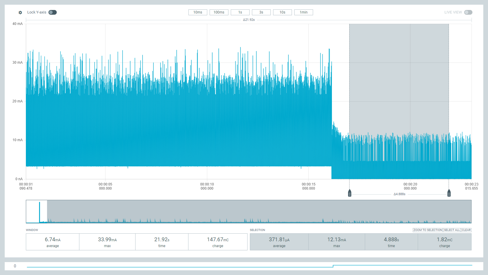
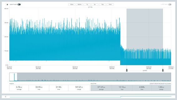
Lock Y-axis 10ms 100ms 1s 3s 10s 1min LIVE VIEW 40 mA 30 mA 20 mA 10 mA 0 nA 00:00:01 00:00:05 00:00:10 00:00:15 00:00:20 00:00:23 090.478 000.000 000.000 000.000 015.655 WINDOW SELECTION ZOOM TO SELECTION SELECT ALL CLEAR 6.74mA average 33.99mA max 21.92s time 147.67mC charge 371.81µA average 12.13mA max 4.888s time 1.82mC charge
工作温度 Topr –40~85 ℃ working temperature 存储温度 Tstg 5~30 ℃ Storage temperature 焊接温度 Tsld 回流焊 260℃不超过 30s ℃ welding temperature Reflow soldering 260 ℃ not more than 30s 手动焊接 300℃不超过 3s Manual welding at 300 ℃ for no more
: -40°C to +85°C Storage Temperature -40°C to +85°C Lead Temperature (soldering, 10s) +260°C Note: EDIP is wave or hand soldered only. This is a stress rating only and functional operation of the device at
g u 0 n l t r p t n t t t t e k 1 2 a / N T A i a a a a a e i i n e z S S S S S e B B A P B B 1 2 Bauteil 74xxxx 74HC374ADW SMD 8BitFlipFlop 24 0,30€ 3 Bauteil 74xxxx 74HCT161 SMD Counter 30 0,70€ 4 Bauteil 74xxxx 74150 Multiplexer,Decoder 21 3,00 € 5 Bauteil 74xxxx 74168
LOW at IOL= 0,8 mA VOL a - 0,4 V Output voltage HIGH at -IO H= 0,2 mA VOH 2,4 - VDO V pF Load capacitance CL - - 50 XSYS (note 8) - 0,4 V Output voltage LOW VOL a Output voltage HIGH VOH 2,4 - VDD V Load capacitance CL
Ich würde 1S xP, ein oder mehrere LiPo Zellen parallel und mit einem briefmarkengroßen StepUp Modul vom Chinesen arbeiten, um auf die 12V zu kommen. 120mA bei 12V sind bei 3V 480 mA und 3V ist schon untere Grenze
6 4 2 0 AVDD_33V AVDD_18V - + - + - + - + DVDD_18DVVDD_33V RJ45_LINK R12 512 3 3 2 2 2 2 2 1 1 1 1 1 8 6 4 2 VREF U3A 74HC04 C29 C18 W X M X D 0.1uF SPD0_LED 1 2 R E _ D I S 2 C 2 O U3B 0.1uF # K U5 4 4 4 4 4 4 4 4 4 3 3 3 3 3 3 3 C20 G S 3 0 0 D 0 0 1 3 1 1 D 1 1 1 LNK0_LED 3 4 E R D X X N X X D D X X N X X D JP5 R G D R R A T T D D R R A T T D VCNTL 49 G B A A A A 32 74HC04 0.1uF FX_SD 1 VREF 50 VCNTL
3.88 inch display for easier maps, messaging, and app navigation • Quad core hardware with 4 GB RAM and 64 GB storage running Android 12 • Worldwide 4G support where available for on grid use • Optional prepaid 2 GB data SIM for hybrid operation with no contracts • Power efficient
[code] It's important for the project as whole to be able to move forward and rely on modern tools and technologies and not be held back by trying to shoehorn modern software on retro computing devices. [/code
c1 8,60 c22,60 d 4,80 e11,20 2,40 S 4,8 IEC a b b 1 b 2 c c1 c2 d e f S Order-No. Type 10.040053 EK 16 20 YEE 2 - 5 dK dK 16,00 16,00 11,04,0 5,00,0011,2000 8,60,002,60,00 4,800011,20 2,40,00 4,8,0 10.045 EK 20 L YEE 2
voltage 9 V TSTG Storage temperature -65 to +150 ⋅C T Operating ambient temperature range SA612A -40 to +85 ⋅C A AC/DC ELECTRICAL CHARACTERISTICS TA=25⋅C, VCC = 6V, Figure 3 LIMITS SYMBOL PARAMETER TEST CONDITION UNIT Min Typ Max VCC Power supply voltage range 4.5 8.0 V DC current drain 2.4 3.0 mA fIN
www.ti.com 6.6 Typical Characteristics At T = 25°C, unless otherwise noted. A 250 1.8 1.6 200 ) V ) 1.4 ( ( g150 i 1.2 l L V t B e 1 -100 u F C V 0.8 50 0.6 0 0.4 0 10 20 30 40 50 60 70 80 90 100 -60 -40 -20 0 20 40 60 80 100 120 Dimming Duty Cycle (%) Temperature (°C) D001 D002 Figure 6-1. FB Voltage
Distortion Voltage TemperatureOptical Fiber Cableppropriate Optical Fiber Cable Module Module (Mb/s, NRZ) (nm) (m) (1) (ns)(1) (V) (°C) (µm) with Fiber-Optic Connectors TOTX196 TORX196 Up to 1000 PCF (200/300) TOCP100Q - BTOCP100X - B DC to 6 800 ±55 5± 0.25 – 40 to 85 - (4) Up to 800 H PCF(200/230
2.0 F ( 160 h 500 C I 1.0 率 300 Ta = 100°C 幅 流 120 増 25 電 タ 流 100 ク 80 0.5 電 −25 流 50 レ 直 コ IB= 0.2 mA 30 40 0 0 10 0 1 2 3 4 5 6 7 8 0.1 0.3 1 3 10 30 100 300 コレクタ・エミッタ間電圧 VCE (V) コレクタ電流 IC (mA) V – I V – I CE (sat) C BE (sat) C 3 30 エミッタ接地 エミッタ接地 圧 I /I = 10 I /I = 10 C B C B 電 1 圧 10 Ta = 25°C 和 電
80% 40V 4822 122 30043 | C 1932 1ONF 80% 40V 4822 122 30043 96 . . 5.5.4. Semi conductors ; P O S N R D E S C R I P T I O N C R D E R I N G C O D E ' W V o o I 5 l B A N S e 4 8 2 2 1 3 0 3 0 6 1 3 : V o 1
tGLQX Output enable low to output transition 5 5 5 ns tEHQZ Chip enable high to output Hi-Z 25 35 40 ns tGHQZ Output enable high to output Hi-Z 25 35 40 ns tAXQX Address transition to output transition 10 5 5 ns 1. Valid for ambient operating tempeAature: T = 0 to 70 °C orCC= 4.75 to 5.5 V or 4.5 to
- /s 1 1 \ Wg V R2-R, 2b plexen Widerstand möglichst verlustlos as = 1 0 -lg (- + -^ + — ); 1 auf den gleichen Wert zu bringen. \4 2 4s/ C =----- = = • [~Rz bei fgist aBgleich Null. (dgyjRi R2 V R2-R ' 3.
557 Philips Semiconductors Linear Products Product specification CMOS 8-bit A/D converters ADC0803/4-1 AC ELECTRICAL CHARACTERISTICS ADC0803/4 SYMBOL PARAMETER TO FROM TEST CONDITIONS UNIT Min Typ Max Conversion time fCLK =1MHz 1 66 73 s 1 fCLK Clock frequency 0.1 1.0 3.0 MHz Clock duty cycle 1 40 60
OCP), Short Load Protection (SLP), and VDD Clamping. ● Battery Chargers for Cellular Phones Company’s Logo is Protected, “JW” and “JOULWATT”●are AC/DC Power Adapter Trademarks of JoulWatt technology Inc. TYPICAL APPLICATION JW1501A/B Rev.0.4 JoulWatt Proprietary Information. Patent Protected. 1 Unauthorized
the same data back. Apple IIe #2: Hardware Protocol for Doing DMA 1 of 9 Apple II Technical Notes H 4 T C 2 A A L D L 7 A O A A H D T D T V D A L N A E T S T S D U O I E B / D C m I V I r D C g L M M i O R D C X c 8 U L l A U A B S I E S a U H O n R I L t - D 7 E S c 0 A ( L P u D M O F ( A T e U R O I B K M C l T 6 R D 5 p A A S A A L G L - 1 A I N A e R I I T ( u T R D U T S N U U i I A K M M C B F B M T I S Y N C E K E D O D R A F - O E R 7 4 L S 2 4 4 2 5 6 2 of 9 Developer Technical Support November 1988 Though the differences
Collector Current 20 mA Transistor Power Dissipation 75 mW IR Diode Peak Forward Current (Pulse Wide = 10S, 300 pps) 1 A Diode Power Dissipation 100 mW Phototransistor Collector-Emitter Voltage 30 V Phototransistor Emitter-Collector
circuit. 1. Maximum Ratings (Ta = 25°C) Characteristics Symbol Rating Unit Storage Temperature Tstg −40 to 85 °C Operating Temperature Topr −40 to 85 °C Supply Voltage V CC −0.5 to 7 V Input Voltage VIN −0.5 to CC + 0.5 V Soldering Temperature T 260 (Note 1) °C sol Note 1: Soldering time ≤ 10 s (More than
This chip integrates a 128 MHz arm-cortex M33 processor, an RISC-V coprocessor, and a power-saving 2.4 GHz multiprotocol radio chip. The Bluetooth LE 6.0, Matter, Thread, Zigbee, NFC, and IEEE 802.15.4 radio protocols can be used, as can also proprietary 2.4 GHz protocols. . . . [/c] ### Phoenix
> Microchip maXTouch - Zwei-Seiten-Touchscreen > Am Stand von Microchip zeigte man einen Touchscreen, der dank geschickter > Polarisierung je nach Einfallswinkel des Betrachters unterschiedliche Inhalte > präsentierte
E D N E WD 1 (M) / R F WD 1000 (M) T I Operating Manual S E T P L N V S K D I F G T C P H K S L S E E V L T L WD 1 (M) / WD 1000 (M) WD 1 (M) WD 1000 (M) Equipment overview 1 Display 2 UP button 3 DOWN button 4 Temperature button III I II III 5 Temperature
0 VDC −3 µADC Leakage (All Data Buffers) V = 5 V 3 µA OUT DC DC SOURCE V OUT Short to Gnd, A= 25˚C 4.5 6 mA DC SINK V OUT Short to CC, TA=25˚C 9.0 16 mA DC POWER SUPPLY CC Supply Current (Includes fCLK= 640 kHz, Ladder Current) V REF/2 NC, T A=25˚C = and CS 5V ADC0801/02/03/04LCJ/05 1.1 1.8 mA ADC0804LCN

 Bild
 Bild

 Bild
 Bild