2C-bus, unique START (S) and STOP (P) conditions are defined. • A START condition is defined with a HIGH-to-LOW transition on the SDA line while SCL is HIGH. • A STOP condition is defined with a LOW-to-HIGH transition on the SDA line while SCL is HIGH. The I2C-bus master always generates the START and
a digital volt meter. Extreme attention is devoted to low distortion design. Details are presented for phase and amplitude trimming. An example of the “R2-Pro” is found in Chapter 12. 9.10—A High Performance Phasing SSB Exciter: The design of a very high performance
likely been purchased with the minimum amount of memory possible then the chips swapped out for higher-capacity versions. It's a hack that has a history, and it often works — but not if component shortages or a desire for higher profits mean you're using RAM that doesn't meet the requirements of the
acquisition of all assets of Saetta Labs, a Boulder, Colo.-based developer of ultra-low phase noise oscillator technology. The transaction, which closed April 20, integrates Saetta Labs’ capabilities into Marki Microwave’s expanding operations and portfolio of high-performance RF solutions
with another pin selected The HBM current waveform appears as follows when as a return. After three high-going and three low- dissipating into a pure short. going pulses across each pin pair, the component is 8.0 checked for damage. This damage typically takes the 7.0 form of a leakage current or of an
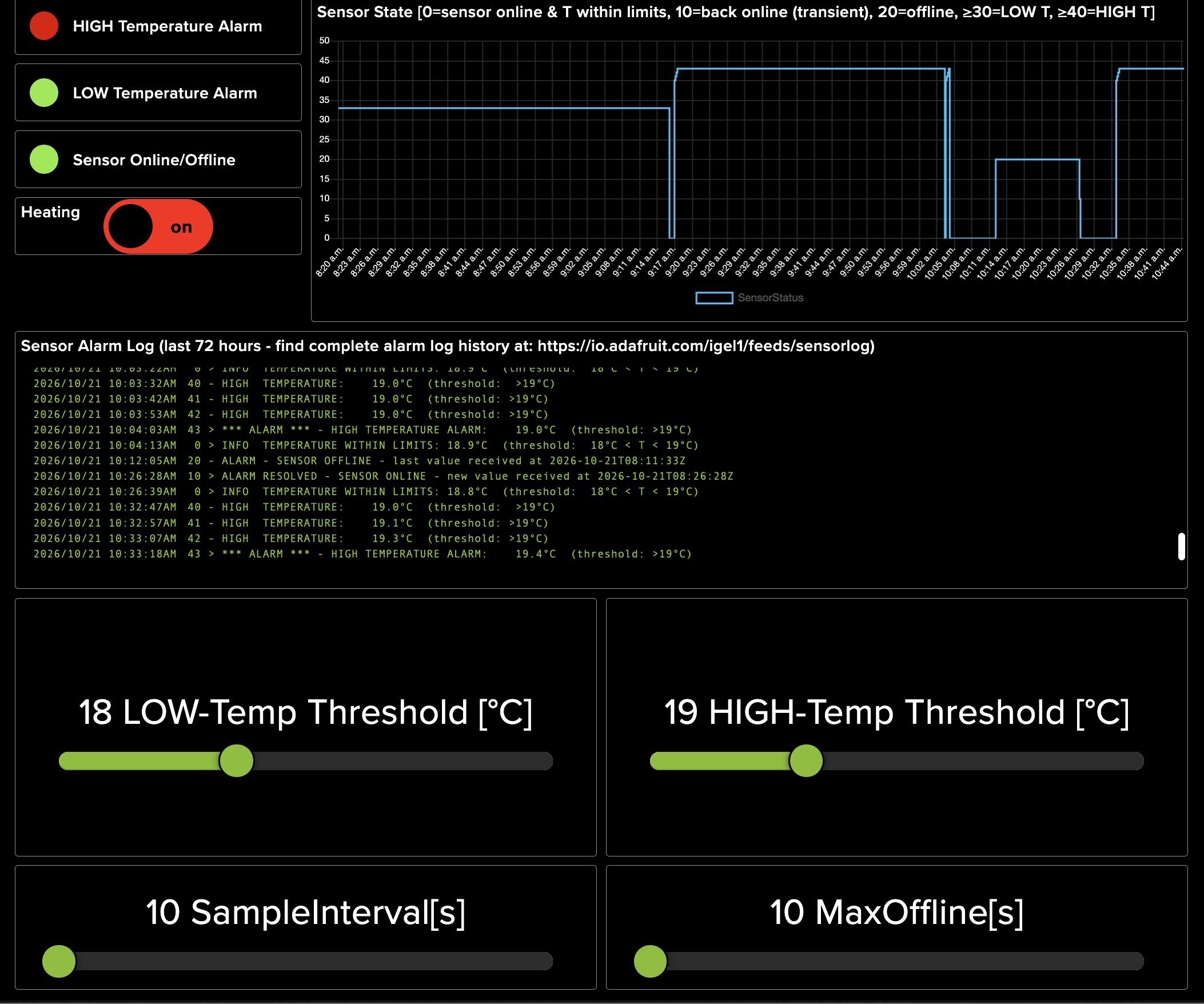
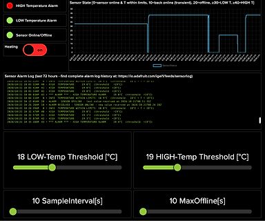
HIGH Temperature Alarm
LOW Temperature Alarm
Sensor Online/Offline
Heating on
Sensor State [0=sensor online & T within limits, 10=back online (transient), 20=offline, >=30=LOW T, >=40=HIGH T]
SensorStatus
Max Unit b Condition AVPL tAS Address Valid to Program -ow O 2 µs tQVPL tDS Input Valid to Program)Low 2 µs tVPHPL tVPS VPP High to Progtam Low 2 µs VCHPL VCS VCC High tu Program Low 2 µs ELPL CES Chip Enable Low to Program Low 2 µs PLPH tPW Program Pulse Width 95 105 µs tPHQX tDH PProgram High to Input Transition 2 µs tQXGL e OES Input Transition to Output Enable Low 2 µs t o l t Output Enable Low to Output Valid 100 ns bt sLQV(2) tOE Output Enable High to Output Hi-Z 0 130 ns O GHQZ DFP tGHAX tAH Output Enable High to Address Transition 0 ns 2. Sampled only, not
Reise > schicken und an der Empfangsseite ein 1kΩ Widerstand gegen Masse liegt, > dann wird der High-Pegel nur um ca. 3% gesenkt. Und die Serienterminierung wird zum Glück auch nur um 3% verfehlt. > Gleichzeitig geistert aber nicht jeder aufgefangene Störimpuls in > die ›Din‹ der ersten LED. Warum sollte ohne diesen 1k Widerstand irgendwas geistern können? Denn es werden ja beide Pegel (High und Low) niederimpedant aktiv getrieben. > Und bei gerade mal 800kHz sieht das Signal auch bei 12m noch prima aus. Wenn du die Signalform gemessen hast, dann passt das ja.
VIN and no load, I Shutdown current CTRL = GND 1 2 µA SD CONTROL LOGIC AND TIMING V H CTRL Logic high voltage 1.2 V V L CTRL Logic Low voltage 0.4 V R PD CTRL pin internal pull-down 300 KΩ resistor tSD CTRL logic low time to shutdown CTRL high to low 2.5 ms VOLTAGE AND CURRENT REGULATION Voltage feedback
the data on the SDA line has to generate an acknowledge after the recep- mustbe stableduring the high period of the clock. tion of each byte, otherwise the SDA line remains The HIGH and LOW state of the data line can at the HIGH level during the ninth clock pulse only change when the clock signal on
WFSTJPO▯DBUBMPH▯ NEOVOL04E2409E0 Series illustration of NeoCapacitor® Standard Big size PS/K P.19 - 24 High operation temp. Ultra low ESR Standard small size Small size PS/G PS/L PS/H P.15 - 18 P.8 - 14 P.32 - 34 ● Same structure as PS/L ● Same structure as PS/L ● Ultra low ESR, 9mΩ or ● High operation temp. lower and long life Low profile High capacitance ● Higher capacitance compare to F/PS PS/L ● Face down terminal structure P.25 - 28 ● Fillet perceivable after soldering on PWB ● Higher capacitance compare
time type high_low pulse sequence [high_low, PRBS_8bit, PRBS_32bit] Rectangle Voltage rectangle voltage source Symbol: Name Default Value Description VH 1 V voltage of high signal VL 0 V voltage of low signal TH 1 ms duration of high pulses TL 1 ms duration of low pulses Tr 1 ns rise time of the leading edge Tf 1 ns fall time of the trailing edge Td 0 ns initial delay time seq high_low pulse sequence [high_low, PRBS_8bit, PRBS_32bit
. either active high or low by pulling them low or high 12 Version: DM9161-DS-F05 September 10, 2008 DM9161 10/100MbpsFastEthernetPhysicalLayer TX/FXSingleChipTransceiver 7. FunctionalDescription The DM9161 performs all
store.mosaico.ai/products/esp-mosaico ### LILYGO T-Halow P4 – ESP32-P4 mit M.2-2280-Interface und WiFi HaLow Das M.2-Interface hat sich im Bereich der Einplatinencomputer mittlerweile als Quasi-Standard etabliert. Nun gibt es im Hause LILYGO eine Entwicklungsplatine, die – wie in der Abbildung gezeigt – über
bekannte Kombination aus ESP32-P4 und ESP32-C6. Hervorzuheben ist, dass außerdem auch ein Wi-Fi-HaLow-Modul auf der Platine verbaut ist. Wer das Produkt käuflich erwerben möchte, kann dies unter anderem auf AliExpress tun. 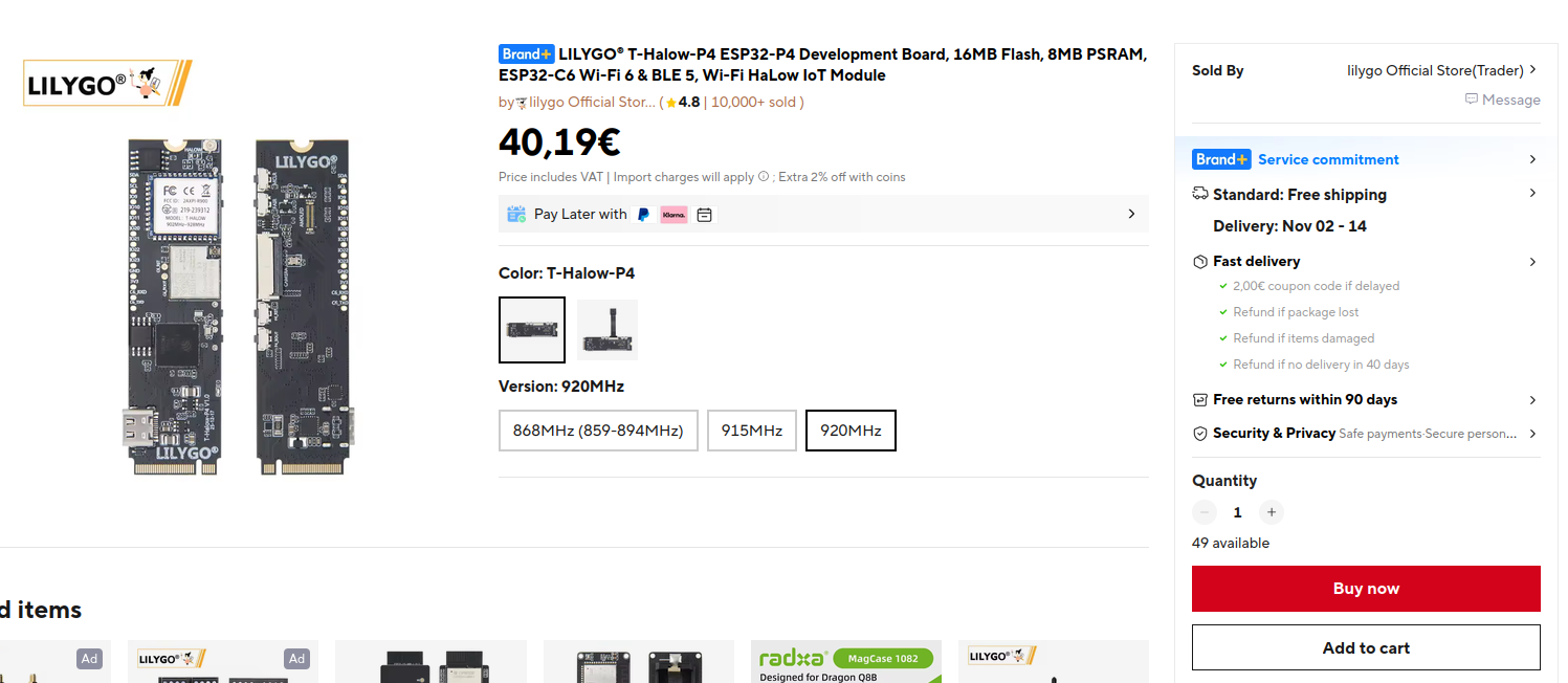 Bildquelle: https://s.click.aliexpress.com
up Converter ME2108 Series General Descriptionÿ▯ Featuresÿ▯ ME2108 Series is a PFM Step-up DC/DC l Low ripple and low noise converter IC with low supply current by CMOS l Operating voltage range0.9V~6.5V process. High frequency noise that occurs during l Output voltage range2.0V~7.0V(step 0.1V) switching
0.765 0.781 V REF PWR Switching Frequency FSW 500 600 700 KHz Short Frequency FSHORT VOUT= 0V 200 KHz High Side MOSFET On-Resistance R DS(ON)-HM 120 mΩ Low Side MOSFET RDS(ON)-LM 100 mΩ On-Resistance High Side MOSFET ILIM-HM 2.5 4 A Current Limit High Side MOSFET I VRUN= 0V, VSWITCH 1 10 uA Leakage Current LEAK-HM = 0V RUN Pin Input Low Voltage VRUN-L 0.4 V RUN Pin Input High Voltage VRUN-H 2 V RUN Pin Pull-Low RRUN 950 KΩ Resistance Maximum Duty Cycle D V = 0.6V 88 % MAX FBK High Side MOSFET TONMIN 100 ns Minimum On Time SST Pin Charge
mode pinMode(pinReceiver, INPUT); // set the laser pin to output mode digitalWrite(pinLaser, HIGH); // emit red laser Serial.begin(9600); // Setup serial connection for print out to console } void loop() { int value = digitalRead(pinReceiver); // receiver/detector send either LOW or HIGH
ratings are measured under board mounted and still air conditions. Symbol Definition Min. Max. Units VB High side floating supply voltage -0.3 625 VS High side floating supply offset voltage VB- 25 VB+ 0.3 V High side floating output voltage V - 0.3 V + 0.3 V HO S B VLO Low side output voltage -0.3 V CC+ 0.3
Lebenszeichen liefert. Am entsprechenden Testpin für den IRQ liegt auch tatsächlich zu keinem Zeitpunkt ein High-Signal an. Hat jemand von euch vielleicht schon mal ein ähnliches Problem gehabt oder eine Idee, wo ich hier ansetzen könnte? Den Boot-Log hänge ich unten mit an.
an die Steuerplatine weiter ob eine Störung vorhanden ist oder nicht. Der STM8 setzt den IRQ auf High wenn alles ok ist. Leider bleibt dieser immer low. Ich habe versucht den I2C Bus von den DLP3440 zu lokalisieren. Bis jetzt bin ich noch nicht fündig worden. Allerdings kommt bei einem DLP3440 ein
Parameter Symbol Test Level Min Typ Max Unit Clock frequency f I 0.5 1 2 MHz PCLK Clock pulse width (high) t I 250 ns HCLK Clock pulse width (low) t I 250 ns LCLK Clock setup time (high)/reset falling edge tSetup I 0 ns No data change tNOOE IV 100 ns Reset pulse width high tHRST IV 50 ns Table 8. 5.0 V
irreversible damage to the device, some restrictions must be followed to prevent overstress on the RF PA: • low-power mode: – For frequencies above 400 MHz, the PaDutyCycle must not be higher than 0x07. – For frequencies below 400 MHz, the PaDutyCycle must not be higher than 0x04. • high-power mode: – For any
wir beim Schaltplan weitermachen? TX_CAN und RX_CAN haben beide die gleiche Signalrichtung. CAN_HIGH und CAN_LOW sollte bidirektional sein. Spannungsversorgung ist kein Label sondern ein Symbol ... -> https://www.mikrocontroller.net/articles/Schaltplan_richtig_zeichnen Rene S. schrieb im Beitrag
und habe mir mal dein Logfile angeschaut. Was gleich auffällt ist das CJ125 DIAG: 0x2855 Heißt: Low Battery. Du solltest dir das Fehlerregister periodisch ausgeben lassen, das gibt wertvoll Hinweise.
Empfänger für die Dauer des Firmware Updates zum schweigen bringen. Erste Idee: der GPS Sender wird low side mit einem ULN2003A abgeschaltet. Vcc bleibt drann. => kann das funktionieren? oder können da Pegel auftreten, welche der NEO-6M nicht so mag und ich einen Hardwareschaden riskiere? Zur Sicherheit
einen 74LVC2G125 und einen 74LVC2G126. Das sind zweifach-Buffer mit Enable beim 125 ist Enable Active-low, beim 126 ist Enable Active-High. Die Enables führst Du alle zusammen auf einen GPIO-Pin und kannst damit zwischen Update-UART und GPS-UART umschalten. fchk
kaufen könnten. Ziemlich hohes Ross für eine Nation die sich zwischen unterwürfigem Betteln nach high tech und Abschottung gegen den Untergang des eigenen Industriemuseums befindet. Und da jetzt wieder 'das ist alles subventioniert' kommt: Subventionen regen uns nur dann auf wenn ein anderer das
Michael K. schrieb im Beitrag #8019201: > China ist längst eine high tech Nation. Bestenfalls Teile von China. Aber auch wird noch ordentlich vom Ausland eingekauft und kopiert. Eigene Innovation ist eher rar. > Und da jetzt wieder 'das ist alles subventioniert
Hallo, ich möchte gern folgendes Netzteil abgeben: HP6624A Kanal 1&2 Low: 0-7V 0-5A or High 0-20V 0-2A Kanal 3&4 Low: 0-20V 0-2A or High 0-50V 0-0.8A OVP und OCP einstellbar Jeder Kanal kann als Downprogrammer ~110% seines Nennstroms als Senke, jedoch nur
: Erst Low-Byte, dann High-Byte Schreibzugriff: Erst High-Byte, dann Low-Byte Des weiteren ist zu beachten, dass es für all diese 16-Bit-Register nur ein einziges temporäres Register gibt, so dass das Auftreten
ca. 0,2*Vcc) anliegt. Detaillierte Informationen darüber, ab welcher Spannung ein Eingang als 0 ("low") bzw. 1 ("high") erkannt wird, liefert die Tabelle DC Characteristics im Datenblatt des genutzten Controllers. + Logikpegel VCC [V] Low [V] High [V] 5 1,0 3,5 3,3 0,66 2,3 1,8 0,36 1,26 Die Abfrage
/t10wh von Everlight. Ich hab etwas ähnliches beobachtet wenn eben kein Signal anliegt, oder der High Pegel länger als ~300µs dauert, ich denke, die AGC Schaltung in diesen Bausteinen schwingt dann, wobei es bei mir eher im Bereich von 20 Mhz war.
> Manchester ist auch nicht Gleichspannungsfrei. Wie meinst du das? Die Dauer der Phasen mit High- und Low-Level ist immer gleich, d.h. du kannst das Signal über einen Kondensator schicken, ohne dass der Pegel abhängig vom Dateninhalt weg driftet.
Deswegen sagte ich ja: theoretisch korrekt, praktisch irrelevant: zB MAX232: Über 2.4V wird high erkannt, unter 0.8V low. praktisch alle Datenblätter sagen, dass die Eingangsseite TTL-Kompatibel ist, selbst der uralte SN75189 (aus 1973). um peda zu zitieren: Man kann nur nicht die maximale
potentialfrei. Ich hab das Singal mit dem Oszi vermessen (siehe Anhang) Ruhepegel 26 Volt (High / Idle) Signal: 14 Volt, also ~12 Volt weniger Ein "Paket" dauert etwa 1700 ms Es kommt alle 10 Sekunden so ein Paket. Die kürzesten Pulse sind ungefähr 0,4 ms breit => deutet sehr klar auf
under 1.2 W/cm2 laser irradiation - Tandem device embedded in UAV winglet powers a propeller under high-power laser [/c] ### Leicht recyclierbarer Zink-Ionen-Superkondensator. Neuigkeit Nummero zwei für „Freunde der Drohne“ ist ein Superkondensator, der einerseits „rigide“ ist, andererseits aber
architecture helps reduce conversion losses and is a major reason BG2B is designed to be Silicon Labs’ lowest-power Bluetooth LE SoC to date. With ~1.1 µA EM2 current (16 kB RAM retained), lower MCU active current, and very low Bluetooth LE transmit and receive currents, BG2B helps developers extend battery
Micropython aufgrund des grossen Speichers (16MB Flash + 32MB PSRam) und der Performance (2*360MHz + 40MHz Low Power Copro) gut geeignet zum Experimentieren und Lernen. Seit der Version 1.27.0 in Micropython unterstützt (P4+C6). Auch sonst ist die Ausstattung brauchbar, Display-Anschluss, Camera-Anschluss
ESP32, Dual-Core, no internal Flash, Chip Revision v3 > ESP32-U4WDH ESP32, Dual-Core, 4MB Flash, High Temperature > ESP32-DOWDRH2-V3 ESP32, Dual-Core, no internal Flash, 2MB SRAM, High Temperature, Chip Revision v3 > ESP32-PICO-V3 ESP32, Dual-Core, SiP Series, 4MB Flash, Chip Revision v3 > ESP32
Conditions Characteristics Symbol Min Typ. Max Unit Supply Voltage V CC 4.75 5.0 5.25 V High Level Output Current I ― ― −150 µA OH Low Level Output Current OL ― ― 1.6 mA 1 2001-08-10 TORX193 3. Electrical and Optical Characteristics (Ta = 25°C, V CC = 5 V) Characteristics Symbol Test Condition
external L.O. Noise figure at 45MHz SR00098 is typically below 6dB and makes the device well suited for high Figure 1. Pin Configuration performance cordless phone/cellular radio. The low power consumption makes the SA612A excellent for battery operated equipment. Networking and other communications products
, JANPTX1N5558UG, JANPTX1N5629AUJ, JANPTX1N5665AUG, JANPTX1N5907UG and JANPTX1N5907UJ. With a high peak pulse power rating of 1.5 kW and clamping response times measured at less than 100 picoseconds in internal tests, . . . [/c] Interessant ist, dass Microchip in der offiziellen Presseankündigung
darüber, dass es eine neue, inoffizielle Version mit Unterstützung für den Raspberry Pi 5 gibt. ### HaLowLink 2 – neuer WiFi HaLow-Accesspoint Der HaLow-Standard nimmt langsam, aber sicher an Fahrt auf. Nun steht ein neuer Router ante Portas, der ein brandaktuelles Morse Micro MM8108-Modul verwendet und
market. Reference Voltage Precision: (Ta=25°C) 0.8V±1.5% (Ta=-40°C to +105°C) ±2.0% BD9615MUV-LB is a low side MOSFET controller with Frequency Range: 100kHz to 2500kHz high withstand voltage (60V). It is suitable for circuits Operating Temperature Range: -40°C to +105°C requiring low side FET such
desired, the corresponding circuitry can be disabled, enabling the Power Amplifier to deliver the highest output power available, Table 47 Table 47 Power Amplifier Modes, PAM PAM1 PAM0 Power Mode Comment Note 0 0 Low power Highest stability 0 1 Medium power Medium stability 1 0 High power Low
mention: • mLRS: mLRS project offers an open source 2.4GHz & 915/868MHz & 433MHz/70 cm LoRa-based high-performance long-range radio link, which provides bidirectional serial connection combined with full remote control • TBS Crossfire: A pioneering commercial LoRa-based system that helped prove
reduced range compared to traditional LoRa modulation. These applications prioritize: • Ultra-low latency: Sub-10ms control latency enables competitive racing and precise freestyle maneuvers. • High update rates: 250-500Hz represents the sweet spot for most freestyle flying, balancing responsiveness
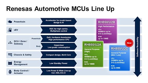
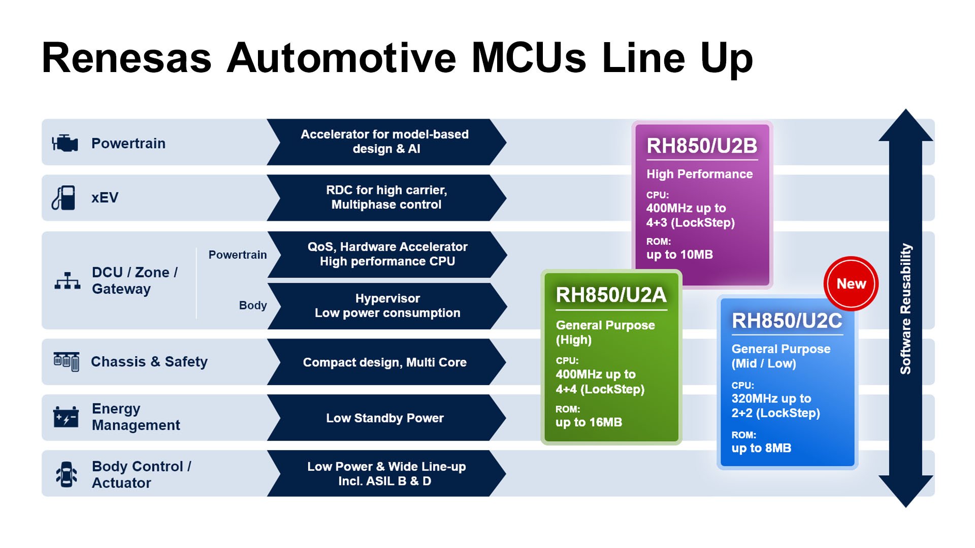
Renesas Automotive MCUs Line Up
Powertrain
Accelerator for model-based design & AI
xEV
RDC for high carrier, Multiphase control
DCU / Zone / Gateway
QoS, Hardware Accelerator High performance CPU
Body
Hypervisor Low power consumption
Chassis & Safety
Compact design, Multi Core
Energy Management
Low Standby Power
Body Control / Actuator
Low Power & Wide Line-up Incl. ASIL B & D
RH850/U2B
High Performance
CPU: 400MHz up to 4+3 (Lockstep)
ROM: up to 10MB
RH850/U2A
General Purpose (High)
CPU: 400MHz up to 4+4 (Lockstep)
ROM: up to 16MB
RH850
Spezifikationen äußert man sich im Hause Renesas folgendermaßen: [c] The SLG46801 integrates two high-speed analog comparators, configurable lookup tables, counters and delays, 10kHz and 25MHz oscillators, voltage-tolerant GPIOs, and an I²C-compatible serial interface. These resources support sensing
monochrome and color versions, Nexora is designed for applications that require sharp images at very high speeds. These include high-resolution machine vision, intelligent traffic systems, and outdoor surveillance. At the heart of Nexora is Teledyne e2v’s proprietary backside-illuminated (BSI) pixel
Preliminary Preliminary Product Description SSW-124 Stanford Microdevices SSW-124 is a high perfomance Gallium Arsenide Field Effect Transistor MMIC switch DC-6 GHz High Isolation housed in a low-cost surface-mountable 8-pin ceramic package. SPDT GaAs MMIC Switch This single-pole, double-throw

 Bild
Bild
 Bild
Bild
 Bild
Bild