was davon merkt. Codecs und Algorithmen in Hardware sind nun nicht direkt eine neue Erfindung. AES in Hardware (für die Verschlüsselung) gibt’s schon sehr lange.
second cannot be easily executed. Outputs The command "ESC Y M number" redefines one or several inputs as outputs. In this case the more significant inputs are used as outputs. 'ESC Y M 3' switches IN8, IN7 and IN6 as outputs OUT1, OUT2 and OUT3 for example. Each line can be controlled individually using
is connected to the GM amplifier as the reference voltage for the FB pin regulation. Therefore, although a PWM signal is used for brightness dimming, only the WLED DC current is modulated, which is often referred as analog dimming. This
durch die man es anscheinend deaktiviern kann. Im Dabla des TDA1591 ist zu lesen: "Applicable as source selector for AM/FM/cassette switching" und "Muting (pin 8) MUTE att mute attenuation (pin 8) V8 < 0.4 V − 80 − dB" Scheinbar lassen sich beide ICs abwechselnd stumm schalten, deshalb
value of the characteristic impedance of the line minus +5.0V +5.0V the output impedance of the driver as close as possible. R 1 R 1 Table 1 lists the values of the series termination resistor RD R2 Z0 CABLE R2 available with the PACSZ1284. R2 C0 R0C Pull-Up Resistor The resistor R1 is a pull-up resistor
Write) In application systems, either a real 8-bit bus (with 8-bit address) is used or Port 2 serves as page register which selects pages of 256-byte. However, the distinction, whether Port 2 is used as general purpose I/O or as "page address" is made by the external system design. From the device’s point
and negative terminals are connected as shown as below.According to the connection, you can get the positive and negative output voltages for your loads. I/P + +V E IN PS1 R L I/P - COM I/P + PS2 R L I/P - -V File Name:RSD-30-SPEC 2018-01-
Sheet on the T6963C is recommended, if this document is unclear. (don’t read the original data sheet, as it is very poor) 2. Basics of Writing to, and Reading from the T6963C For all of the following, so long as your microcontroller takes more than 200ns to do an instruction, you arn’t going to violate
at “SDA” pin becomes a voltage potential divider. As a result, the acknowledgement would not be possible to attain a valid logic 0 level in “SDA”. “SDA ” and “SDA ” are tied together and serve as SDA. The “SDA ” pin must be connected to IN OUT IN act as
at “SDA” pin becomes a voltage potential divider. As a result, the acknowledgement would not be possible to attain a valid logic 0 level in “SDA”. “SDA ” and “SDA ” are tied together and serve as SDA. The “SDA ” pin must be connected to IN OUT IN act as
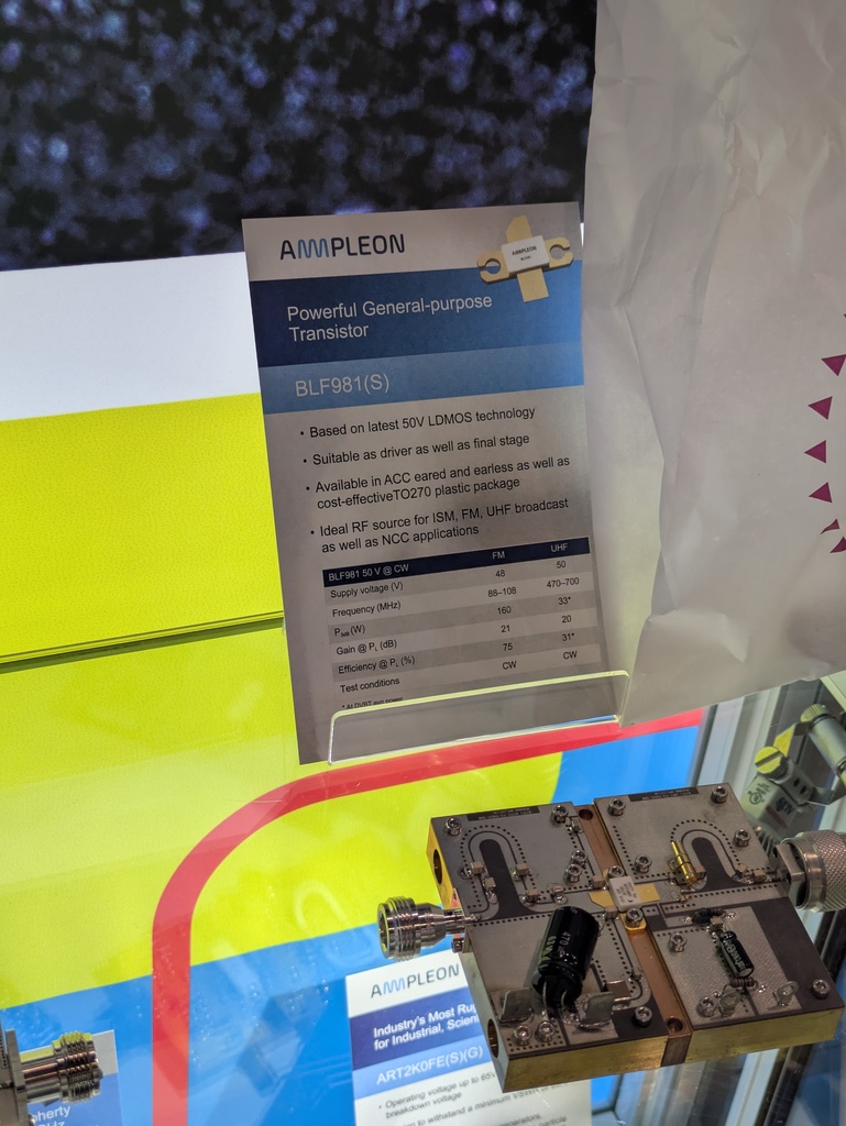
AMPLEON
Powerful General-purpose Transistor
BLF981(S)
Based on latest 50V LDMOS technology
Suitable as driver as well as final stage
Available in ACC eared and earlier as well as cost-effective TO270 plastic package
Ideal RF source for ISM, FM, UHF broadcast as well as NCC applications
BLF981 50 W @ CW
the retainers (5) 1–10 – Unfasten the retaining plate from the back of the scale – Unwind the cable as far as required and then refasten the retaining plate Leveling the Scale Using the Level Indicator § Level the scale using the level indicator as a guide. $ Extend the leveling feet (turn clockwise)
or coating material, which contains halogenated solvents, is not allowed. In general, all adhesives as well as filling and coating materials need to be tested and validated by the customer. • All other soldering methods are at the customer’s own risk. • Strong forces which may affect the coplanarity of
Rev. 4.1 — 22 August 2016 8 of 31 NXP Semiconductors PCA9532 16-bit I C-bus LED dimmer 6.4 Pins used as GPIOs LEDn pins not used to control LEDs can be used as General Purpose I/Os (GPIOs). For use as input, set LEDn to high-impedance (00) and then read the pin state via the INPUT0 or INPUT1 register.
text... be as honest and helpful." *Wait, actually the instruction says:* "Remember to output ONLY your response... do not output other text... be as honest and helpful." *Wait, let me re-read the instruction carefully
Operating Current it is hold until the next sampling. The sampled The operating current of OB2502x is as low as voltage is compared with reference voltage Vref 680uA (typical). Good efficiency and les than (typical 2.5V) and the difference is amplified. The 75mW standby power is achieved with the low error
DC Layout A summary of the key layout steps, in order of priority is: 1. Place the input capacitors as close as possible to the IC with wide, short traces to the VIN and PGND pins. Every millimeter makes a difference! Minimize the area of the loop from CIN to VIN and PGND back to CIN. 2. Place the inductor, as close as possible to the SW pin of the device, keeping the switch-node area as small as possible. 3. Place output capacitors from the inductor, returning to the PGND close to the input capacitor. Again
hardware protocol for doing direct memory access (DMA) on the Apple IIe and Apple ][ and is meant as a guideline for developing peripherals which do DMA on these machines, not as a specification for future Apple products or revisions. This Note covers the timing differences between the Apple ][ and
389/stmicroelectronics_cd00044334-1205474.pdf 12 Stück im Stangenabschnitt EUR 10,- * STM VN5E160AS-E Einkanal-Highside-Schalter 140 mOhm mit analogem Current Sense Ausgang. Eingang 4,5-28 V, Ausgang bis 1 A, automotive-tauglich. Package SO-8. https://www.st.com/resource/en/datasheet/vn5e160as-e.pdf
our knowledge and experience of typical requirements concerning the 7. Property Rights areas, serve as general guidance and cannot be estimated as binding statements about the suitability for a customer application. The responsibility for the applicability and use in a particular customer design is always
(Pulse Width Modulation) speed control features of Noctua’s 4-pin PWM fans. Detailing aspects such as connector types, pin configuration or RPM speed signal output as well as signal specifications and circuit design questions, it enables engineers to implement PWM based speed control for Noctua fans
ein Beispiel, das lustigerweise ein Art aliasing Effekt hat: [code] #!/python import tkinter as tk import matplotlib.pyplot as plt from matplotlib.backends.backend_tkagg import FigureCanvasTkAgg from matplotlib.animation import FuncAnimation import numpy as np root = tk.Tk() fig, ax =
with the help of Perplexity 2026-01-31 mchris ''' import serial import csv import matplotlib.pyplot as plt import matplotlib.animation as animation from datetime import datetime, date import numpy as np import sys from collections import deque import matplotlib.dates as mdates # ----------------------
Steckbrett oder auf ein entsprechend gerouetetes Board stecke kann. Auf github gibst du an, dass "rvusb as a later step" angedacht ist, auch darauf bin ich sehr gespannt. :-) auch wenn ich da mittlerweile meinem Clone des EASY-PDK verhaftet bin (einfach weil in der Handhabung pragmatischer). Vllt. wird
WriteRegister (BME280_SOFT_RESET_ADDR, BME280_SOFT_RESET_VALUE)) return FALSE; Delay_ms (10); /* ** Wait as long as the chip is copying calibration data to image registers. ** For this purpose we read the status register. ** If still copying, wait for additional 10 ms. */ l_ReadStatus: BME280_ReadRegisters
access requires knowledge of the secret and the capability of computing and transmitting a 160-bit MAC as authorization Secret and data memory can be write-protected (all or page 0 only) or put in EPROM-emulation mode ("write to 0", page 1) "
meistens auch bei den Bundles dabei ist. Damit kann ich auch das Config-Flash flashen, sowohl über AS als auch JTAG. Bei den aufgeführten Boards würde ich keinesfalls das mit dem EP1C3 nehmen. Das ist der uralte Cyclone 1, der noch nicht einmal Hardwaremultiplizierer hat. Und für den Preis von 30,
input to output mode, the DR register has to be written first to drive the correct level on the pin as soon as the port is configured as an output. 3 3. Do not use read/modify/write instructions (BSET or BRES) to modify the DR register External interrupt function When an I/O is configured as Input with
which is connected with of the + and U- (V-, W-) terminals, restrains and spares serge voltage being as the connection of the snubber circuit (Capacitor / CS / about 0.1 to 10μF) for the voltage absorption with the neighborhood as possible between Points of intersection between the + and U-, V- and W-
angedachten 2S6P, den ich zur Not auch auf 1S12P umfrickeln kann habe ich 12 bzw in 1S 24Ah zur Verfügung as bei 120mA rechnerisch 100h Leuchtbetrieb ermöglichen würde. Der augenblickliche 2S ist bereits mit einem passenden USB-C Ladeanschluss sowie einer Schutzschaltung(BMS) versehen.
nice, high-quality recording of "Fireside Al" Maitland reading Frederick Forsyth's "The Shepherd" as heard traditionally on "As it Happens" on CBC every Christmas eve beginning in 1979" https://en.wikipedia.org/wiki/The_Shepherd Gerhard
Software Development Kit (SDK) including graphical configurability and S32 Design Studio software, as well as broad support from IAR Systems, Arm, Software, Green Hills, and other partners. 4. This refers to region addressable by Arm CM4 Code bus and is used to cache code as well as data in this region
development kits contain different C Compilers for optimum support of device variants. Cx51 is used as a generic term for: C51 Compiler for classic 8051 devices, 8051 IP cores, Dallas Contiguous Mode, and other extended devices CX51 Compiler for Philips 8051 MX and SmartMX C251 Compiler for 251 devices
threads, depending on the state of the Threads-mode toggle. That total is further classified as: running; sleeping; stopped; zombie Line 2 shows CPU state percentages based on the interval since the last refresh. Where two labels are shown below, those for more
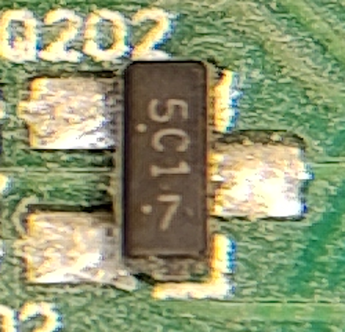
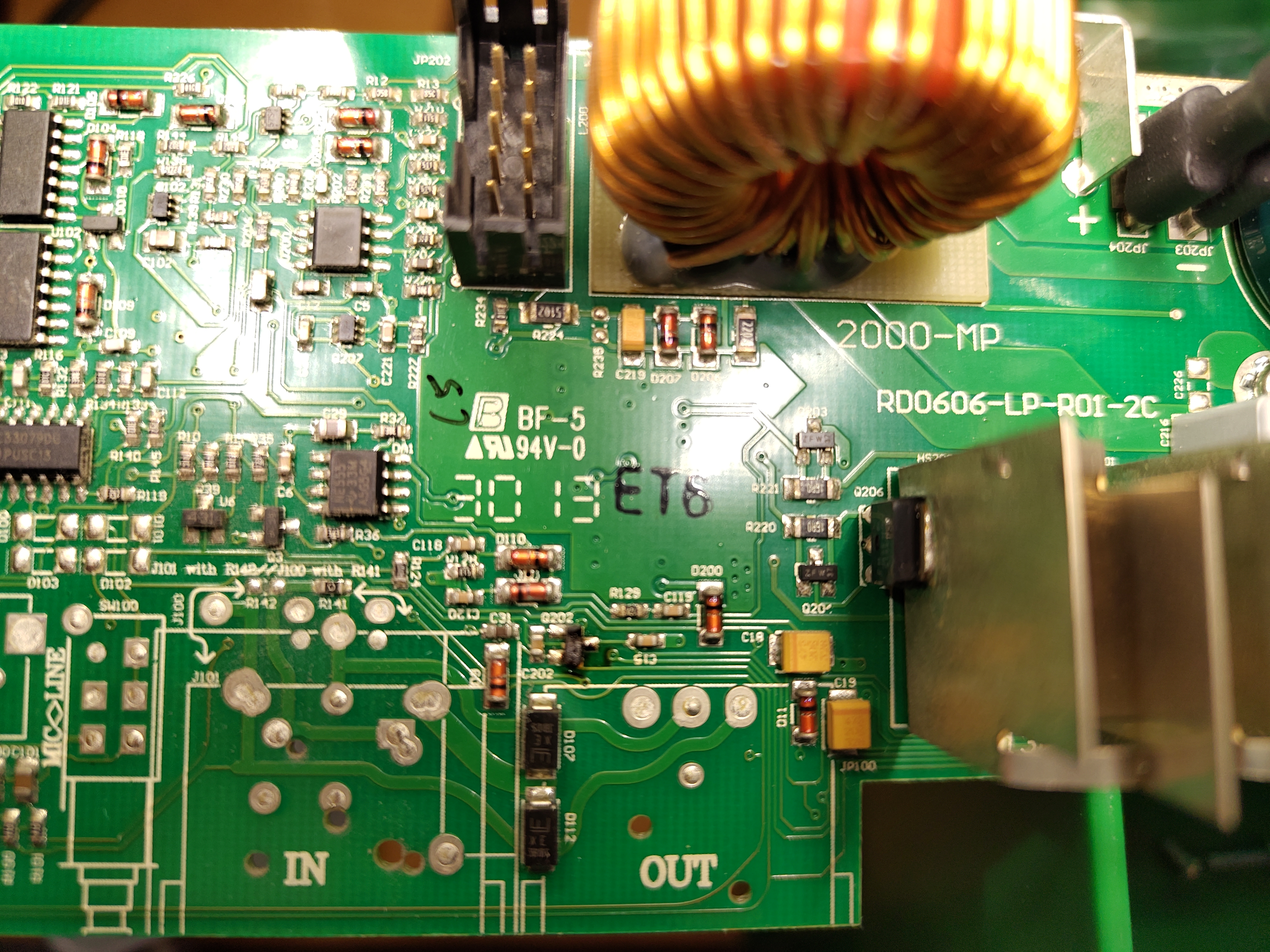
erstes und zweites Bild. Wenn ich das richtig interpretiere, handelt es sich um eine Spannungsreferenz "AS431" im SOT-23-Gehäuse. Wenn ich mich nicht verrechnet habe, sollten sich da da 29 Volt (1+100/9,1)*2,500V als "Fußpunkt" für den Optokoppler an der "Anode" einstellen, kommt mir recht viel vor. Tatsächlich
mode to control the output current at any output voltage at or below the voltage regulation target as long as the auxiliary winding can keep VDD above the UVLO turn-off threshold. V + V)×Na× R1 In JW1501A/B, the ratio between Tdem and Tsw O F Ns R1 + R2 in CC mode is 1/º. Therefore, the average output
1 (V CL1) is defined as the voltage between the VDD and VC pins at which V CO goes from “L” to “H” when the voltage V1 is then gradually decreased. Overcharge hysteresis voltage 1 (V HC1) is defined as the difference between
Erfahrung ist es ein Ding der Unmöglichkeit zwei Taktquellen > identisch hinzubekommen. Kommt auf as Teilerverhältnis an. Bei den 1 kHz klappt es perfekt. Die 16.384 MHz sind wohl kein Zufall. > Daher wurde ja auch die PLL erfunden, um eine > Taktquelle auf eine andere zu synchronisieren. Daher
relaxation oscillator are transmitted to the function versatile of today's low-frequency instruments. As well selector switch after passing through the relevant as having a wide range of frequencies, they offer a amplifier. The sinusoidal voltage is obtained from the variety of different timing functions
board as described in the section Board Replacement. If the trace is not visible, continue with item 3-2.15. 3-2.15 Replace the CC board as described in the section Board Replacement. 3-2.16 Locate and identify
inspiring countless colourful Raspberry Pi creations, and the release of new handheld maker devices such as the Cardputer Zero and Hackberry Pi, there has been an increase in small SPI and I2C displays being used as the main display for Raspberry Pi. To help them look more responsive during boot, we have developed
means no response time guarantee on failures, and failures that do not block a release, so treat it as a floor. The team has said it wants to move toward tier 2. [/c] ### EMV: Spin-out mit Seminaren Im Hause Mesago arbeitet man daran, das EMV-Feld effizient zu beackern. Neben den parallel zu den
program- mabledead-time,andprogrammableover-currentpro- tection. Comprehensive protection features such as 14 Lead SOIC protection from failure of a lamp to strike,filament fail- ures, as well as an automatic restart function, have 14 Lead PDIP (narrow body) beenincludedinthedesign.TheIR2156isavailablein
or more scripts to execute, along with data files that these scripts can use. These scripts are run as root so that they can access all of the file systems. I’ve already referred to running apt upgrade, but for custom software updates, you could create an artefact containing a .zip file and a script to
possible merger of their power semiconductor operations, it was learned Thursday. The move comes as automotive parts maker Denso Corp. is seeking to acquire Rohm, whose special committee is believed to be currently examining the acquisition offer. Rohm is expected to consider which offer would increase
fixed to the machine frame with an M8 hexagon socket-head screw. To measure the power supply, proceed as follows: Æ Switch the placement system off at the main switch. Æ Loosen the M8 lock screw on the underside. Æ Pull the unit out as far as the stop. WARNUNG Make sure that the main power cable and supply
Hochspannungs-Widerstände hoher Stabilität The RVCU series offers a voltage coefficient of resistance (VCR) as low as 25 ppm to 50 ppm, depending on resistance value, providing a lower-error alternative to conventional high-voltage chip resistors which may have VCR up to 300 ppm and beyond, for best performance
stability. Operating over a standard 10–20 MHz frequency range, the device consumes 1W during warm‑up and as little as 0.2W at +25 °C in steady state, helping extend battery life while maintaining a clean, stable reference under specified operating conditions. [/c] ### Microchip LAN878x and LAN888x
provides a digital output that indicates the • 11-Bit Battery Voltage Setting presence of the AC adapter as well as an analog output which • 6 Bit Charge Current/Adapter Current Setting indicates the adapter current within 4% accuracy. • 8A Maximum Battery Charger Current The ISL88731 is available in a small
long-pin or short-pin configurations. Designers combine three 9-pin connectors with one 8-pin that acts as a keying guide for assembly, creating a 35-pin bus. [/c] ### HiRose KMA01 – 6GHZ-Antennensteckverbinder robuster Bauart Im Automotivebereich kann es schon einmal ruppig zugehen. Mit dem KMA01 steht
: [c] Stackpole Electronics, Inc.’s TNC Series of NTC thermistors provides a proven alternative as a robust alternative to multilayer thermistors for temperature sensing applications. Utilizing thick film technology, the TNC Series delivers superior mechanical strength, consistent part thickness across
of 200000 samples per second. 2 Resolution of an ADC One ADC step in the digital domain is defined as 1 least-significant bit (LSB), and this is often used as the reference unit for ADC specifications. It is also the measure of the resolution of the converter, because it defines the number of counts

 Bild
Bild
 Bild
Bild

 Bild
Bild