-
Bild
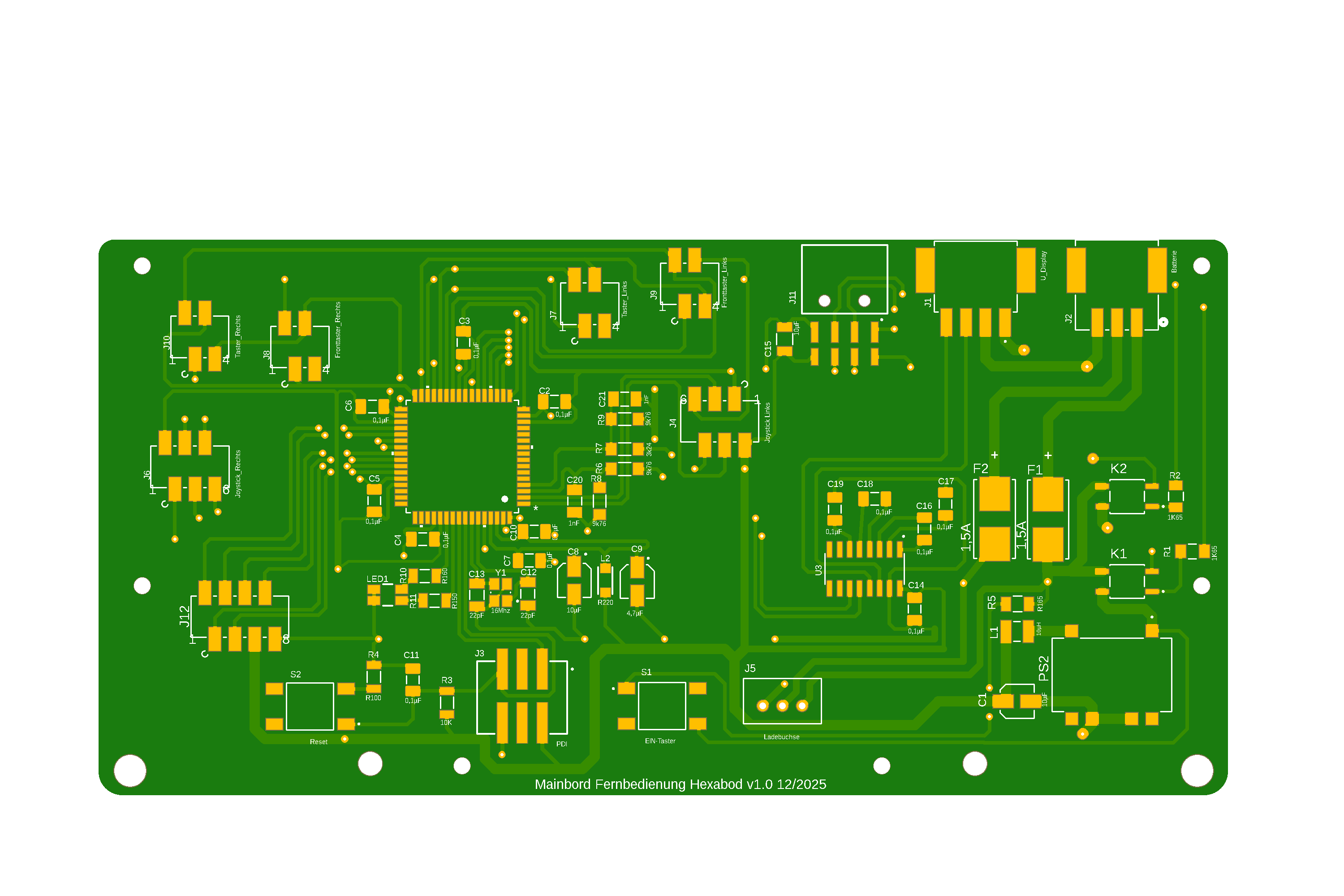
PCB-Layout einer Fernbedienung
C21, C22, C25, C26, C27, C28, C29, C30, C31, C32, C35, C36, C37, C38, C39, C4, C5, C6, C7, C8, C9, C10, C12, D6, D7, D8, D9, F1, F2, F3, F4, K1, K2, L1, L2, L3, L4, L5, R1, R2, R3, R4, R5, S1, S2, S3, S4, S5, S6, S7, S8, S9, S10, S11, S12, U1, USB, W1, Mainbord Fernbedienung Hexabod v1.0 12/2025, Reset, FBI, EfS Tester
in „erste Platine, bitte um Hilfe/Kritik“ · Platinen · · Layouts
-
PDF
pm2534ocr.pdf
S T 8-1 8.1 Méechanital parts cisa0s saewen cennawe coe werenae we: BA] 8.2 Electrical parte #926 10usiis iss oxssioweseswessavees B-3 9. CIRCUIT DIAGRAMS AND PRINTED CIRCUIT BOARDS LAY-OUTS 9-1 10. GLOSSARY OF TERMS 10-1 11. M O D I F I C A T I O N S 11.1 Hardware modifications ....scceeeeccccnccreccaceece
in „Pjilips PM2519“ · Markt ·
-
PDF
pm2521ocr.pdf
manual orautomaticselection),thecurrentsaredetermined by thesignals R N G C , R N G D and RNGE: ImA —10V —10V OV 200 (2 —0,2V 200.00 22 ImA —10V —10V OV 2kQQ. — 2V 2.0000k02 : 100uUA —10V —10V —10V 20k22 - 2V 20.000k22 1TWA —10V —1OV —10V 22 M Q2 — 22V 2.0000M&2 100n A OV OV —10V 20M&2 — 2V 20.000M&2 :
in „Pjilips PM2519“ · Markt ·