-
Bild
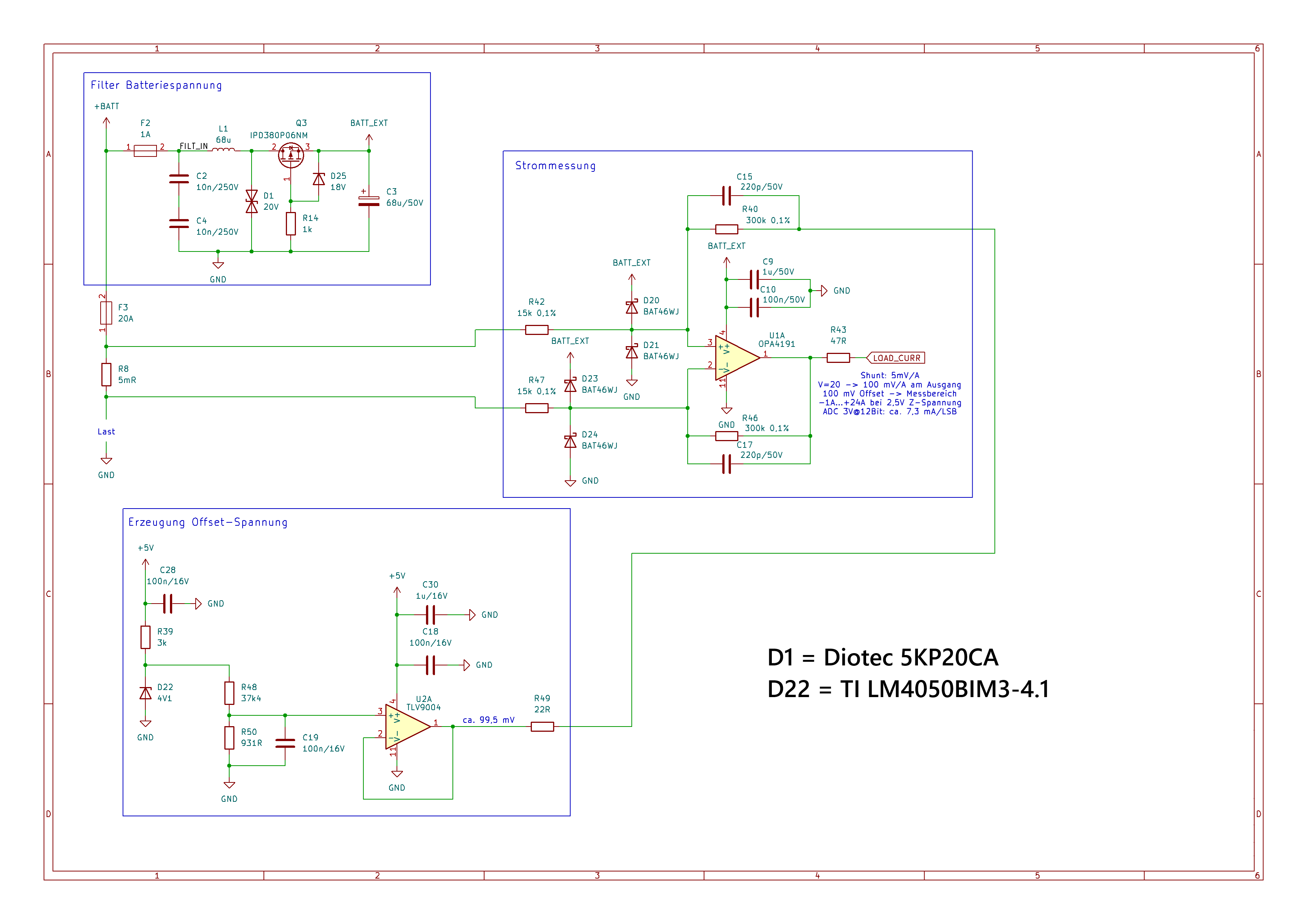
Schaltplan Strommessung und Offset-Spannung
C4 10n/250V, R14 1k, GND, Strommessung, C15 220p/50V, R40 300k 0.1%, BATT_EXT, C9 1u/50V, GND, U1A OPA4191, R43 47R, LOAD_CURR, Strom 5mV/A am Ausgang V=20 -> 100 mV, R42 15a 0.1%, D20 BAT46WJ, BATT_EXT, D21 BAT46WJ, D23, R47 15k 0.1%, BAT46WJ, GND, D24, C17 220p/50V, GND, Erzeugung Offset-Spannung, +5V, C28 100u/16V, GND, C30 1u/16V, GND, C18 100u/16V, GND, R39 3k, U2A TLV9004, R48 37k4, R50 931R, 922 5V1, GND, R49 22R, ca. 99.5 mV
in „Eingangsschutz/Diode mit geringem Leckstrom für OPV zur Strommessung im KFZ“ · Analoge Elektronik und Schaltungstechnik · · Schaltpläne
-
PDF
Orion_Rev_3.0__1_.pdf
IO_B6_H30/DIFFIO_R19P/DQ2R IO_B6_P27/DIFFIO_R28P P27 AD29 IO_B5_AD29/DIFFIO_R47P IO_B5_W29/DIFFIO_R37P W29 INA4_2 J25 IO_B6_J25/DIFFIO_R6P IO_B6_P28/DIFFIO_R28N P28 AD30 W30 J26 P30 AE25 IO_B5_AD30/DIFFIO_R47N/DQ3R IO_B5_W30/DIFFIO_R37N Y22 J27 IO_B6_J26/DIFFIO_R10N/DQS2R/CQ3R,DPCLK10 IO_B6_P30/DIFFIO_R29N
in „Suche Firma die für Privat BGA FPGA reballing macht“ · Markt ·
-
Bild
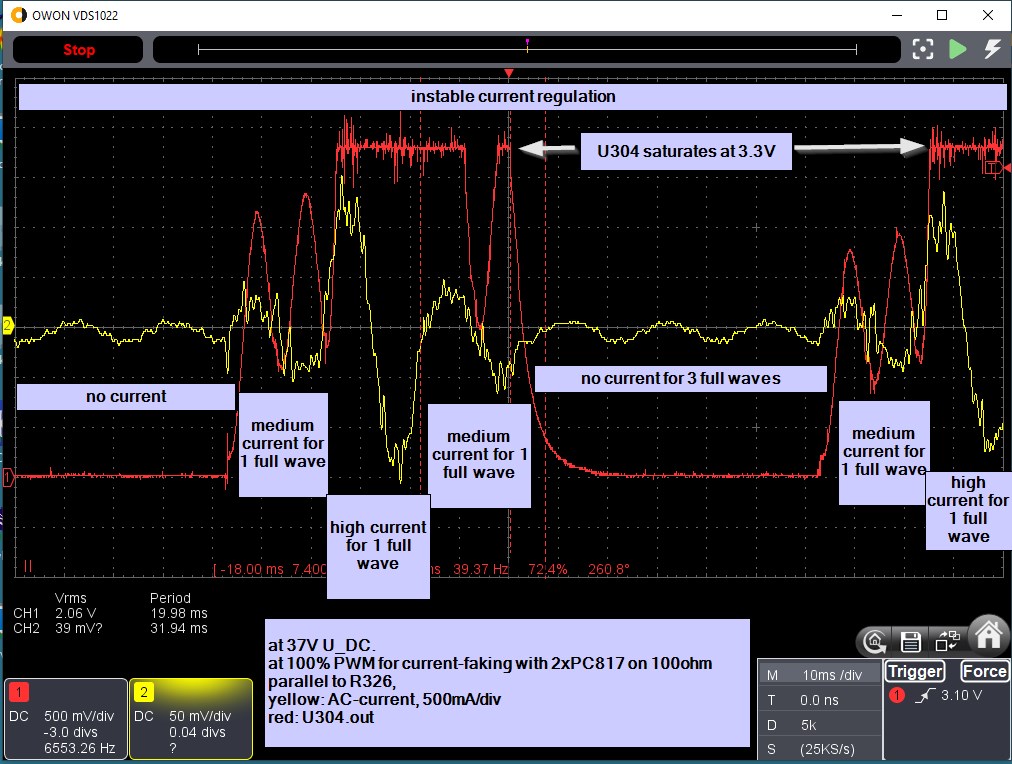
Oszilloskop-Messung instabiler Stromregelung
OWON VDS1022 Stop instable current regulation U304 saturates at 3.3V no current medium current for 1 full wave medium current for 1 full wave high current for 1 full wave no current for 3 full waves medium current for 1 full wave high current for 1 full wave CH1 2.06 V CH2 39 mV? Period 19.98 ms 31.94 ms DC 500 mV/div DC 50 mV/div -6.553 Hz 0.04 div? 39.37 Hz 72.4% 260.8° at 37V U_DC. at 100% PWM for current-faking with 2xPC817 on 100ohm parallel to R326, yellow: AC-current, 500mA/div red: U304 out M 10ms/div T 0.0 ns S 5k (25KS/S)
in „Hoymiles HM-300 für Batteriebetrieb umbauen“ · Analoge Elektronik und Schaltungstechnik · · Oszi-Bilder
-
PDF
TM56E6422-tenxtechnology.pdf
ms @5V WKT 12ms,24ms,48ms,96ms @5V 15.6ms,31.3ms,62.5ms,125ms @5V SFR.RDCTL X V (suggest RDCTL=4ns) OPA V X SFR.OPOF OPOF=0 (POR, CMPP <= OPO) No OPA (CMPP to OPO) OPOF=1 (CMPP <= CIPx ) must set OPOF =1 in emulation (CMPP connect to CIPx) VCC /1.2V / 2V / 2.48V SFR.ADVREFS VCC / 2.48V ADVREFS=1.2V/2V
in „MCU identifikation/Datenblatt - MC9989A0ZQ“ · Mikrocontroller und Digitale Elektronik ·
-
PDF
TM56M152A-tenxtechnology.pdf
MOVLW 16h ; W = 16h MOVWX RAM020 ; RAM[0x020] = W = 16h MOVWX RAM0A0 ; RAM[0x0A0] = W = 16h MOVLW 37h ; W = 37h MOVWX LVRPD ; LVRPD = W = 37h, force LVR/POR disable MOVXW CLKCTL ; read SFR CLKCTL (00Fh) to W MOVXW IRCF ; read SFR IRCF (10Fh) to W MOVLW 0Bh ; W = 0Bh MOVWX CLKCTL ; CLKCTL (00Fh) = W
in „MCU identifikation/Datenblatt - MC9989A0ZQ“ · Mikrocontroller und Digitale Elektronik ·
-
PDF
pm2534ocr.pdf
test lead. R 7 0 1 +Vp wal * CZ i n 2R02 | pa aoe 101 a | F801 103 In i202.7e e4ai ero a v13 i aad | C37 =Va i pe? S a03 e zoe 1208 0G 1210 viz05AWE2VI206BAw6é2 vI2Z07AWEZ c37Saoe a ss[see ee¢seos C U R R S O U R C E 8 6 0 4 2 9 Figure 3.7 Current source 3 - 1 2 The measuring currents are derived from the
in „Pjilips PM2519“ · Markt ·
-
PDF
pm2519ocr.pdf
R25 1% 10K 4821651268 6 2 Pos.nr. Description Orderingcode Ris14 MR25 1% 226K 5321654729 - 1600 PR37 5% 15E 48216514 R1603 MR25 1%5% iM87 5322 116 55535 1604 MR25 % 3K65 32 64587 R1605 MR25 1% 248 5921654515 16076 MR25 1% 953K 5321651368 1 6 0 9 8 M R 2 5 1 % 1 K 2 7 5322 116 50555 2 5 3 R 1 6 1 0 M
in „Pjilips PM2519“ · Markt ·