Kurzeinführung - IBFWiki http://www.friedrich-eichenzell.de/ibfwiki/index.php?title=Kurzeinf... Die Bauteile 74HC04_DIN 74HC08_DIN und 74HC121 , den Widerstand R_MET_2,2K_0204 , den Kondensator C_FOLIE_0,022µF_RM7,62 und die Steckverbinder K1...K4 finden Sie in der Bibliothek Standard.SYM3001. Die Kontakte K1 ...
Seite 3) - https://www.ti.com/lit/ds/symlink/sn54f04.pdf - https://www.ti.com/lit/ds/symlink/sn74hc04.pdf - https://www.ti.com/lit/ds/symlink/sn54als04b.pdf HC und ALS sind sogars langsamer.
3) > - https://www.ti.com/lit/ds/symlink/sn54f04.pdf > - https://www.ti.com/lit/ds/symlink/sn74hc04.pdf > - https://www.ti.com/lit/ds/symlink/sn54als04b.pdf > > HC und ALS sind sogars langsamer. Ich sach doch, wenige Tausend Picosekunden später.... ;-) Ok, Danke für die Links, kommen sofort
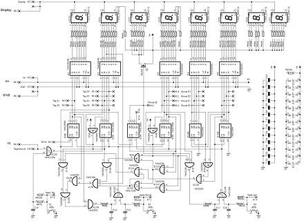
O U3A O 3 6 B 1CLK ~1Q B ~1CLR O 1 74HC32D_2V GND X 74HC74D_2V U4A X U2A 74HC08N_2V C X C 31 15 74HC04D_2V 10 U1B R T ~2PR 12 2D 2Q 9 11 8 D 2CLK ~2Q D ~2CLR 13 U5A 74HC74D_2V U7A 74HC86D_2V 74HC00D_2V E E 10 U6B ~2PR 12 2D 2Q 9 F F 11 8 2CLK ~2Q ~2CLR 13 74HC74D_2V G G 0 1 2 3 4 5 6 7 8
138 15 AC 139 12 AC 151 18 AC 153 10 AC 163 5 AC 191 21 AC 373 25 AC 374 16 AC 541 34 ACT 373 14 HC 04 1 HC 10 15 HC 11 18 HC 14 3 HC 20 4 HC 27 23 HC 30 3 HC 42 6 HC 85 26 HC 86 3 HC 107 21 HC 109 21 HC 112 2 HC 123 43 HC 133 17 HC 137 2 Keramik HC 138 1 HC 139 26 HC 151 14 HC 153 5 Keramik HC 154
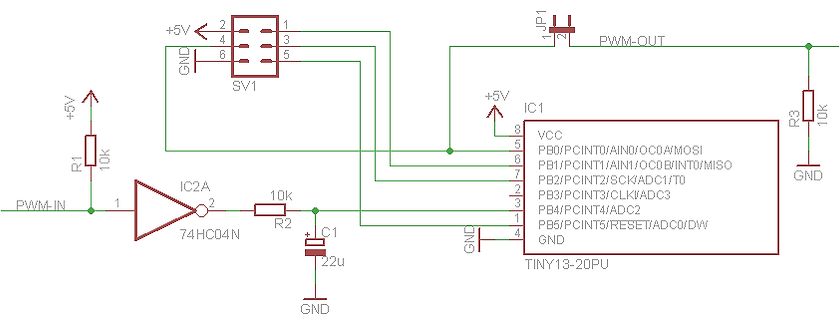
product_peizo.htm 10Vss sollten die aber auf jedenfall verkraften. Mit ein paar parallel geschalteten HC04 Inverter, am besten als H-Brücke geschaltet um 10Vss zu erzeugen, und mit 2,75kHz versorgt sollte sich dieses Piepser als nicht zu überhörender Alarmgeber verwenden lassen.
V C C C B Reset 74HC74 74HC74 74HC74 DSTM3 1 1 1 S1 Reset Implementation = Reset U19A 1 2 DSTM5 74HC04 S1 Clock3 U12D 12 Implementation = Clock3 11 13 R6 DSTM7 74HC00 S1 Clock3I 1k Implementation = Clock3I GND_0 GND_0 A Mescheltana GmbH A Title FM0 Dekoder 0 Copy and paste the GND_0 circle in Size Document
alles in China fertigen. Ausserdem hat Nexperia durchaus auch interessante Sachen jenseits des 74HC04. Schau dir z.B mal ein NEH2000BY an. Ein Schaltregler der mit 35uW minimaler Inputpower auskommt muss man erstmal koennen. .-) Vanye
(ja , ich habe 100nF Kondensatoren drin und ich habe auch 10 µF ElKos drin). Ich hatte auch ein 74HC04N drin - den habe ich aber wieder rausgeworfen, da sinnlos und icvh immer invers denken musste.
Frequency tolerance is VDD=5.0V expressed in percentage, typical ±0.5% or in parts per millions 14 MC 74HC04 (ppm), ±5000ppm. (MOTOROLA) 1 2 3 4 7 Resonant Impedance: The value of impedance the crystal exhibits in the operating resonant circuit. R OUT GND 1.0MΩ RESONATOR Aging: The relative frequency change
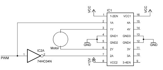
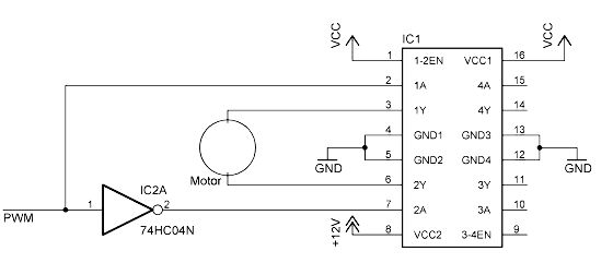
Übersetzungen für entsprechende Ungenauigkeiten. Die Elektronik besteht bis dato aus zwei l293d, einem 74hc04 und einem Atmega8. Testweise könnte ich die Geschwindigkeit des Schlittens schon auf 650 us pro Halbschritt bringen. Das war bei 12 Volt, das Spendergerät des Motors liefert 42 V, also sollte ich sogar
Außerdem beschreibt der TCXO-Hersteller in einer Application Note die Signalwandlung, z.B. durch einen 74HC04-Inverter mit Rückkopplungs-Widerstand. Utilize Clipped Sine Waveform in Circuit Design http://www.taitien.com.tw/db/pictures/modules/CMS/CMS060207001/AP20100105-Utilize%20Clipped%20Sine%20Waveform
Pulse Test 6 1997 6-43 MIC94030/94031 Micrel Typical Applications SS* +5V S D MIC94030 G a On L Off 74HC04 * Substrate must be connected to source Figure 1. Power Switch Application +12V Internal Resistor G S Open Drain SS* Output MIC94031 D d a L * Substrate must be connected to source Figure 2. Power Control
disablen? 2. *Bluetooth* Gibt es jemanden, der den Bootloader hier mit so einem Bluetooth-Modul HC-04 oder HC-05 erfolgreich einsetzt? Ich würde gerne wissen, ob das Out-of-the-Box geht, oder was man ggf. beachten muss. 3. Unterschiedliche *Baudraten* Ich möchte in der APP eine andere BAUD-Rate
P/A BA-6209 70406209 BA-6209 I.C. CA-3086 70423086 TRN ARRAY CA-3280E 70403280 CA-3280 I.C. CD-74HC04 70410004 HEX INVT. BUFFER CD-74HC27 70430027 3 INPUT NOR CD-74HCT11 70430011 CMOS TRIPLE INPUT AND ? Page 15 ORIGINAL ALTERNATE FIELD IN-HOUSE IN-HOUSE REPLACEMENT ORDER NUMBER NUMBER NUMBER NUMBER
P/A BA-6209 70406209 BA-6209 I.C. CA-3086 70423086 TRN ARRAY CA-3280E 70403280 CA-3280 I.C. CD-74HC04 70410004 HEX INVT. BUFFER CD-74HC27 70430027 3 INPUT NOR CD-74HCT11 70430011 CMOS TRIPLE INPUT AND ? Page 15 ORIGINAL ALTERNATE FIELD IN-HOUSE IN-HOUSE REPLACEMENT ORDER NUMBER NUMBER NUMBER NUMBER
werden, wie z.B. ein Für Grundton-AT-Quarze sind soge- CMOS-Gatter sind darauf ausgelegt, zwi- 74HC04. Damit sind Frequenzen bis über nannte aperiodische Oszillatoren, d.h. Os- schen 2 Zuständen umzuschalten. 20 MHz erzeugbar. zillatoren ohne zusätzliche Selektionsmit- Durch Gegenkopplungswiderstände
to create higher quality pictures when there is an S-video circuit that uses one inverter of a 74HC04 package to create a input available on the monitor. crystal oscillator and another inverter to buffer the oscillator Flicker and drive other loads. The logic family must be a CMOS type In a VGA conversion
U502D 3 AUDIO_IN/OUT R513 C504 C505 R516 R518 33p 33p SPDIF 1 2 3 4 5 6 9 8 2 1 330 330 150 D 100n 74HC04/SO 74HC04/SO 74HC04/SO 74HC04/SO 100n C506 V 7 7 7 7 R517 270p COAXIAL D 91 R515 1M P R535 7 FB120 0 0 0 G R Ha up tp la t te / M a in Board – D V D - F ro n te n d U N D RFVCC I G S e C732 EC702 +5V
Working with events measured in nanoseconds requires the 74S04, but significantly faster than the 74HC04. In fact, the LT1223 has completely finished its transition the greatest caution, prudence and respect for Mother before the 74HC04 even begins to move! Linear circuits Nature. Absolutely nothing should
only the sequence generation, the dynamic simulation and the Environment Sensor-Board FPGA-Board 74HC04 (Driver) Modulator Codegenerator S Sequencegenerator y0 simulation c x e TL071 (Anti-Aliasing-Filter) I PC (LNA) (8 Bit ADC) r 2 A D y1 e 2 i R E1 INT A/D - u Controller 8 WR 4 & INT Controller y2 A
gezeigt. Als Verstärker wird der Inverter SN74HCU04 eingesetzt, der eine ungepufferte Version des SN74HC04 ist und damit eine Sonderstellung in der HCMOS-Familie einnimmt. Die Innenschaltung aller HCMOS-Schaltungen ist mehrstufig ausgeführt, wobei der Ausgang durch zwei hintereinander geschaltete Inverter
gezeigt. Als Verstärker wird der Inverter SN74HCU04 eingesetzt, der eine ungepufferte Version des SN74HC04 ist und damit eine Sonderstellung in der HCMOS-Familie einnimmt. Die Innenschaltung aller HCMOS-Schaltungen ist mehrstufig ausgeführt, wobei der Ausgang durch zwei hintereinander geschaltete Inverter
VCC CS 8 ANALOG • D INPUT CHANNELS • OUT • LTC1296 CLK P CH7 D IN COM REF+ REF– SSO 50k 50k 5V 74HC04 0.1 F V D CC IN 100 CLK VOUT LTC1257 LOAD 0.1 F GND V REF DOUT V D CC IN 100 CLK VOUT LTC1257 LOAD 0.1 F GND V REF DOUT 1257 TA02 12-Bit Single 5V Control Systemwith Shutdown 5V 100k 10k 10 F 2N3906
used. The diode in parallel with the R LED speeds the turn-off 2 of the optocoupler LED. 220 Ω 74HC04 TOTEM-POLE LED OUTPUT LOGIC 3 GATE) 4 Figure 17. CMOS gate drive circuit. 14 www.agilent.com/semiconductors For product information and a complete list of distributors, please go to our web site. For
programming, you should add terminator (“ENTER” or “0x0d 0x0a”) to the program. It’s different from HC-04 and HC-06 (They don’t need terminator). (2) The most common commands for HC-03 and HC-05 are: AT+ROLE (set master –slave),AT+CMODE( set address pairing) ,AT+PSWD (set password). If you want the master
pins (NC) to GND. Remarks 1. The inverters shown in the above application circuit example are the 74HC04 (data rate < 2 MHz) or the 74AC04 (2 ≤ data rate < 10 MHz). 2. Inverters B1 to B3 in the above application circuit example are shown in the figure below. B1 to B3 EQUIVALENT CIRCUIT 12 V + 47 F/25 V
18V - + - + - + - + DVDD_18DVVDD_33V RJ45_LINK R12 512 3 3 2 2 2 2 2 1 1 1 1 1 8 6 4 2 VREF U3A 74HC04 C29 C18 W X M X D 0.1uF SPD0_LED 1 2 R E _ D I S 2 C 2 O U3B 0.1uF # K U5 4 4 4 4 4 4 4 4 4 3 3 3 3 3 3 3 C20 G S 3 0 0 D 0 0 1 3 1 1 D 1 1 1 LNK0_LED 3 4 E R D X X N X X D D X X N X X D JP5 R G D R R A T T D D R R A T T D VCNTL 49 G B A A A A 32 74HC04 0.1uF FX_SD 1 VREF 50 VCNTL B TEST1 31 DVDD_33V 51 VREF DGND 30 PWRST# FX_SD_TEST X1 52 DVDD33 PWRST# 29 EECS C24 R15 R16 X2 53 X1 EECS 28 EECK 0.1uF 54 X2 EECK 27 EEDIO 49.9/1% 49.9/1% LNK1_LED 55
18V - + - + - + - + DVDD_18DVVDD_33V RJ45_LINK R12 512 3 3 2 2 2 2 2 1 1 1 1 1 8 6 4 2 VREF U3A 74HC04 C29 C18 W X M X D 0.1uF SPD0_LED 1 2 R E _ D I S 2 C 2 O U3B 0.1uF # K U5 4 4 4 4 4 4 4 4 4 3 3 3 3 3 3 3 C20 G S 3 0 0 D 0 0 1 3 1 1 D 1 1 1 LNK0_LED 3 4 E R D X X N X X D D X X N X X D JP5 R G D R R A T T D D R R A T T D VCNTL 49 G B A A A A 32 74HC04 0.1uF FX_SD 1 VREF 50 VCNTL B TEST1 31 DVDD_33V 51 VREF DGND 30 PWRST# FX_SD_TEST X1 52 DVDD33 PWRST# 29 EECS C24 R15 R16 X2 53 X1 EECS 28 EECK 0.1uF 54 X2 EECK 27 EEDIO 49.9/1% 49.9/1% LNK1_LED 55

 Bild
Bild
 Bild
Bild
 Bild
Bild
 Bild
Bild
 Bild
Bild