Passend zu diesem Forum: https://debeste.de/upload/544bdca5eb6be4b4e51af8744e6c0152.jpg
betreffend: + Verstellmöglichkeit TON Frequenz + Lautstärkenregelung + entweder feste Verzögerung im ms Bereich, oder die Möglichkeit selbst das zu verstellen und immer wieder mit Trial & Error zu arbeiten. In einem Nachbarforum hat mir innerhalb von 12h jemand angeboten, das bauen zu können. Nur der
Zeig mir mal einen Temperatursensor, bei dem sich eine Änderung der Gehäusetemperatur innerhalb von 1ms auf den Messwert auswirkt. Immerhin haben Wäremleitfähigkeit, thermische Übergangswiderstände und Wärmekapazität des Temperatursensors noch ein Wörtchen mitzureden, bevor die Temperaturänderung beim
mir mal einen Temperatursensor, bei dem sich eine Änderung der > Gehäusetemperatur innerhalb von 1ms auf den Messwert auswirkt. Du hast es mal wieder nicht verstanden, was ich schreibe. Es kommt bei einee Messfolge von 1 rpo sekunde nicht mehr wesentlich auf die Ansprechgeschwindigkeit des Temp
Devices, Inc. Cyrix is a trademark of Cyrix Corporation. ALI is a trademark of Acer Laboratories Inc. MS-DOS, WINDOWS NT are registered trademarks of Microsoft Corporation. OS/2 is a trademark of Internal Business Machines Corporation. UNIX is a trademark of Bell Laboratories. 10 Table of Contents Table
über moderne AVX/SSE Erweiterungen oder > Cache Architektur. Das gilt vielleicht bei MSVC und der MS Libc (Ich glaube das war msvcrt oder so?). GCC / Clang mit der glibc sind sehr gut optimiert. Die glibc nutzt auch teils ASM wenn es wirklich was bringt, inklusive AVX/SSE. So einfach kriegt man da
damit umgehen. Ich versuche in meinem Code, ihn zu vermeiden. Ich hatte mal in einem übernommenen C51 Code einen kniffligen Fehler damit. Der vorherige Programmierer hat in einer Funktion auf 0 getestet. Nun ist aber 0x0000 beim 8051 eine gültige Adresse in XDATA und der Linker hat dort auch brav ein
will be transferred to USB host via HID ‘Input Report’. USB host will keep polling HID report every 1ms. CM6206 can also transfer four bytes from USB host to MCU. This is accomplished by a ‘Set Output Report’ HID request issued by USB host.CM6206 will then assert MINT to inform MCU to read them. CM6206
20 µs (2) /CS High to next Instruction after Reset tRST 30 µs Write Status Register Time tW 15 20 ms Byte Program Time (First Byte) BP1(4) 20 50 µs (4) Additional Byte Program Time (After First Byte) BP2 2.5 10 µs Page Program Time PP 0.7 3 ms W25Q64FVxxIG 60 Sector Erase Time (4KB) W25Q64FVxxIQ & SE 400 ms W25Q64FVxxIF 45 Block Erase Time (32KB) tBE1 120 1,600 ms Block Erase Time (64KB) tBE2 150 2,000 ms Chip Erase Time CE 20 100 s Notes: 1. Clock high + Clock low must be less than orC.qual to 1/f 2. Value
power The expected current is: 3000 current from the voltage source will follow the surge 1 = 50 + 8= 51.7A and V R = 8 × 51.7 = 414V discharge (called “follow-current” or “power-follow”). In AC circuits, this power-follow current may not be cleared at a The maximum voltage appearing across the terminals
Source) 3 mA Output Current Sink I 10 mA IOUT(Sink) Overcurrent Transient Tolerance IP 1 pulse, 100 ms 100 A Nominal Operating Ambient Temperature TA Range E –40 to 85 ºC Maximum Junction Temperature T (max) 165 ºC J Storage Temperature Tstg –65 to 170 ºC Isolation Characteristics Characteristic Symbol
1: Package thermal resistances were obtained using the method described in JEDEC specification JESD51-7, using a four-layer board. For detailed information on package thermal considerations, refer to www.maxim-ic.com/thermal-tutorial. RECOMMENDED DC OPERATING CONDITIONS (TA= -40°C to +85°C) (Note 2)
floats, 1.4k flash use), On all pins, with new implementation., Disabled (burn bootloader req'd), 8ms, 1x Wire, Master or Slave (least Flash & RAM), USART2 (alt): TX PF4, RX PF5 (>28 pin only), Disabled (recommended), No delay before window "opens", Use last FLMAP section, lock FLMAP, provide PROGMEM_MAPPED
Refresh All Read/Refresh access or Update All Write/Update access is permitted is permitted Wait Wait 1 ms Wait Wait 10 ms to allow internal to allow internal 1 ms EEPROM read 10 ms EEPROM write YES Wait until pervious YES Wait until pervious EEPROM read cycle is finished EEPROM write cycle is finished is
Watchdog Oscillator Cycles Typical time-out (CC = 5.0V) Typical time-out (VCC = 3.0V) Number of cycles 0ms 0ms 0 4.1ms 4.3ms 512 65ms 69ms 8K (8,192) Main purpose of the delay is to keep the AVR in reset until it is supplied with minimum Vcc. The delay will not monitor the actual voltage and it will be required
trip delay in 10 effect) of its primary task. The voltage used to represent km cable is about 0.1 ms while 5 kbps implies 0.2 ms bits is also converted (changed). Extra bits (called start nominal bit time, and a need to sample during the and stop bits) are added to each byte before it is second half
and CV022 49/ 0 : 50/ 0 : ; These bit locations in CV029 must not be necessary for packet processing 51/ 0 : =0x6 PRIADD: EQU CFGRES ; set if primary address match 52/ 0 : =0x7 CONADD: EQU CFGACC ; set if consist address match 53/ 0 : 54/ 0 : ; Default values for some CVs 55/ 0 : =0x0 DEF019: EQU 0 ; consist
Setting These bits selects the start-up time between power-on and code execution. Value Description 0x0 0ms 0x1 1ms 0x2 2ms 0x3 4ms 0x4 8ms 0x5 16ms 0x6 32ms 0x7 64ms 6.8.4.7 Application Code End Name: APPEND Offset: 0x07 Reset: - Property: - Bit 7 6 5 4 3 2 1 0 APPEND[7:0] Access R R R R R R R R Reset 0 0
8XRBngl2xhXxwOyJhWM3E6TGzhJdiaGRazQebAASlVengqPyyrQqAiytBlGoOe0lkzkEY2AAXIpdDDaWmYdr7JgIMGQYg0HA8XiubRMIL5A16DCQXBRDBgeiGKgAEwYxwAricFZMGW8tpy1AZdu5fnK7I4bKrlRqtsxyIjEsQHa4CDIaDQEAErglIOw1CFMjJla9maTA4W+IJrqW7Ck6LcKQWwpWGnlbtcmyDW+4S1SymSK9Go51BEXI+9KjZpuOGgB7MwgWlUGh64jUBOESwhhfYNjz+hL4Wkddg2LpJAQW6ZNhAA Anbei noch ein Link auf ganz viele Details und Schaltungen mit dem NE555, der vermutlich overkill für Dich sein dürfte: http://pegons-web.de
eine gemessene Temperatur von selbstmitnormalenExemplarenlässtsich 23 °C. Die Lichtblitze dauern 135 ms und die Schaltung mit einer 3-V-Knopfzelle die nachfolgenden Pausen 400 ms. ziemlich lange betreiben. Auf die ähnliche Weise werden auch an- Theoretisch können mitdemSensor Tem- dere Ereignisse angezeigt
MC6809-SBC als Kit aus Thailand: https://www.ebay.com/itm/285784821259?itmmeta=01HW36TXT5VZ4XTC0VS51G74QG&hash=item428a1a4e0b:g:e7wAAOSwKLFfAZjp
Microsoft hat auch sowas, und die lesen > bekanntlich alles mit. Mit oder ohne Recht. Und da wollte MS sein BS noch rechtzeitig aus der Gefahrenzone bringen. Alles klar!
forward current IF(AV) TC= 110 °C, D = 0.50 60 Non-repetitive peak surge current IFSM TC= 25 °C, p = 10 ms, sine wave 500 A Repetitive peak forward current I T = 110 °C, D = 0.50, f = 20 kHz 120 FRM C Operating junction and storage temperature TJ, Stg -55 to +175 °C ELECTRICAL SPECIFICATIONS (T = 25 °C unlessJotherwise
Das interne Reset war die Schwachstelle, es mußte ab 0V erfolgen und die VCC mußte schneller als 10ms/1V ansteigen. Ansonsten blieb er tot. Der Befehlssatz war deutlich komfortabler als bei den einfachen PICs. Ich hab noch irgendwo 2 Samples liegen. https://media.digikey.com/pdf/Data%20Sheets/Fairchild
$ cpm pwd=/home/horo/cpm starting yaze_bin Yet Another Z80 Emulator by AG, final release 2.51.1.1 (MMU,KeyTr,WinSz,MHz) Copyright 1995,1998 Frank D. Cringle. Pagetables Copyright by Michael Haardt. MMU and CP/M 3.1 extensions Copyright (c) 2000,2019 by Andreas Gerlich. Keytranslation Copyright
Zu 80C51 Zeiten hatte ich nie Probleme mit Quarz im Full-Swing Modus. Bei aktuellen µCs im Low-Power Modus gibt es schonmal einige Exemplare, die nicht anschwingen. Ich setze daher in neuen Projekten nur noch
erste Wahl. Wenn man nun als Entwickler ankäme mit "Naja, meistens schwingt das Teil schon nach 10 ms, aber wenn es kalt ist, gibt es Ausreißer bis 2 s.", dann hätte man schon ein Problem.
the LTC4151-2 is not. APPLICATIONS PART PACKAGE FEATURED PIN n TelecomInfrastructure LTC4151 DD10, MS10 SHDN n Automotive LTC4151-1 DD10, MS10 SDAO n Industrial LTC4151-2 S16 SDAO n Consumer L, LT, LTC, LTM, Linear Technology and the Linear logo are registered trademarks of Linear Technology Corporation
Advanced Menu ..........................................................................................51 21.5.1. Advanced Chipset Control Submenu.............................................................52 21.5.2. PNP ISA UMB Region Exclusion Submenu...................................................
ungewöhnlich erscheinen. Bitte folgende Messungen ggf wiederholen und eintragen als L/R Werte: -R3132 (51R) beide Seiten -R3130 (51R) rechte Seite -T3109 Basis (Verbindung R3136-R3135) -VR3103 links Bitte für folgende 51R Widerstände (grün, braun...) den Ohmwert bei abgeschaltetem Oszi im eingebauten
51R, ist 51,2R (auch umgepolt gemessen) R3132 soll 51R, ist 51,4R (auch umgepolt gemessen) > > Was steht auf VR3103 als Beschriftung? > 605 10K Alle Messungen habe ich vorsichtshalber mehrfach
switchable D Domestic appliance D Triggering pulse typ. 125 mA Package: DIP8, SO8 Block Diagram 22 kW/2W BYT51K 230 V ~ R1 D 1 R2 a max R 8 330 kW 1 MW 96 11643 Load 7 6 Limiting Voltage Mains voltage detector detector compensation Automatic retriggering Phase 5 –VS Current control unit TIC detector ö = f (3
eingestellten Zeit fährt der Antrieb mit Rampe auf null. Mögliche Werte: 0: keine Reaktion 1: t 30 ms 2: t 100 ms 3: t 1000 ms 4: t 3000 ms 5: r 30 ms 6: r 100 ms 7: r 1000 ms 8: r 3000 ms P-56 184 – rw Modbus ParityType 0, 1, 2, 3 Possible Values: • 0: No Parity, 1 Stop Bit (N-1) • 1: No Parity, 2 Stop
Klickt man mit der rechten Maustaste darauf, so öffnet sich ein Menü, in dem man die Startzeit (30ms), die Skalenteilung („tick“ = 1ms) und die Stoppzeit (35ms) eintragen kann: Mit „OK“ zeigt sich folgendes Bild des Bereiches von 30 bis 35ms mit einem Tick von 1ms: 17 4.5. Änderung des dargestellten
--- 192.168.1.1 ping statistics --- 4 packets transmitted, 0 received, 100% packet loss, time 3069ms [/code] Also, zusammengefasst: - Alle Geräte, die eine statische IP-Adresse bezogen haben, gehen problemlos ins Internet. - Der Laptop geht ins Internet über Ethernet Kabel mit einer statischen
MULTICAST,UP> mtu 1500 qdisc fq_codel state DOWN group default qlen 1000 link/ether c0:3e:ba:4a:51:38 brd ff:ff:ff:ff:ff:ff altname enp0s31f6 3: virbr0: <NO-CARRIER,BROADCAST,MULTICAST,UP> mtu 1500 qdisc noqueue state DOWN group default qlen 1000 link/ether 52:54:00:86:de:3d brd ff:ff:ff
except when stamped “CONTROLLED COPY” in red. DESCRIPTION: PDIP6 8.51X6.35, 2.54P PAGE 1 OF 1 ON Semiconductor anare trademarks of Semiconductor Components Industries, LLC dba ON Semiconductor or its subsidiaries in the United States and/or other countries. ON Semiconductor
welche Routine, in jeden Schritt hinein geht, und was dabei heraus kommt. Ist die Summe zweier 50 ms-Perioden plausibel? Wenn nein - muss vorher sein. Wenn ja - muss hinterher sein. Sind die Zählwerte in den Registern plausibel? U.s.w. Systematische Fehlersuche, zu der die Kenntnis gehört, was sich
AVRs kannte ich aber schon Assembler und habe entsprechend programmiert – 8085, Z80, 6502, 68000, µC51. AVR-Assembler (der 8-bitter) ist auf jeden Fall etwas freundlicher und einfacher als die teilweise sehr komplexe Adressierung mit vielen Operanden und Ausnahmen der CISC-Architektur damaliger Zeit –
Ich hab auch oft alten C51 Code auf anderen MCs wieder verwendet. Z.B. generisches I2C, SPI mit einfachen IO-Pins. Das spart deutlich Arbeit gegenüber jedesmal den Code für die Hardware-Einheiten anderer MCs umschreiben zu müssen
habe bisher mit ATMega328P nur mit 16 MHz gearbeitet, so war für mich einfacher, mit einem Timer 1 ms-Puls zu bekommen, als mit 20 MHz. Jetzt habe ich mit AVR128DB begonnen, hier sind Beschränkungen solcher Art etwas milder.
Resets aufgerufen wird dann kann das zu sowas fuehren. Ich hatte mal so ein Problem mit einem MCS51 Derivat wo Rueckspeisung ueber einen Gleichstrommotor die Spannung langsam angehoben hat und zu Alzheimer gefuehrt hat. Wenn du sowas nochmal hast dann lies den mal aus. Hast du eine defekte oder
andere schon nicht mehr. Das führt zu zufälligen Befehlen, Parametern und Adressen. In den paar ms die das anhält schafft die MCU erstaunlich viele Befehle abzuarbeiten. Und irgendwann war dann auch was dabei was einen Schreibvorgang im Flash auslöste. BOD gesetzt, nie wieder Probleme gehabt.
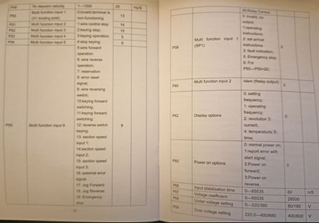
Multi function input 1 13 20: Relay Control
(X1 binding post) 0:invalid, terminal is non-functioning
P51 Multi function input 2 14 0:invalid, no output;
1 wire control stop
P52 Multi function input 3 15 1:operating instructions;
2:keying stop, 3:keying operation
P54 Multi function input 4 5 5:wire forward
C-bus protocol as to how long this delay can be, whereas for a SMBus system, it would be limited to 35 ms. SMBus protocol just assumes that if something takes too long, then it means that there is a problem on the bus and that all devices must reset in order to clear this mode. Slave devices are not then
automatisch auf 0 gesetzt 2~0 WDTCKS [2:0] Auswahl der Watchdog-Uhr WDTCKS[2:0] WDT-Überlaufzeit 000 500 ms 001 250ms 010 125ms 011 62,5 ms 100 31,5 ms 101 15,75 ms 110 7,88 ms 111 3,94 ms 7~5,3 - Reservieren 7.3.5 Ausgangszustand zurücksetzen Wenn der SC93F833X zurückgesetzt wird, kehren die meisten Register
e o . . edi St cat no C 1 O i o o s l 1 0 eul G 0 e U l T e ng U n i A G D edi St cat no C xa M mm51. 0=t mm2. 0=t mm360. 0x8x51 l epa Tevo me R reziral oP B8131# M3 v r e p ur r a e i t S 6 u C 5 2-R0.4± 0.05 0 SS V ) 3 H MDC V 3 1 " FE RI 0 7 D ± 6 l 5 DD 0 e e r . e 3 DD 0 i i z 0 x 2 D W l S a A

 Bild
Bild
 Bild
Bild
 Bild
Bild